Electronics Production
1. Week Assignments
group assignment:
- characterize the design rules for your in-house PCB production process
- submit a PCB design to a board house
individual assignment:
- make and test an embedded microcontroller system that you designed
- extra credit: make it with another process
2. Prior Knowledge
I have not made a PCB before.
3. Work!
This week I'll be using the Gerber2Png KiCad plugin and Mods to drive the PCB mill.
There are two machines at the Waag to make PCBs:
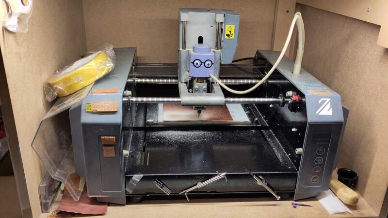
Roland Modela MDX20
It is basically a tiny version of the Shopbot CNC we used last week. Henk told us it is (one of?) the oldest machine at the lab and it still runs fine. It can be operated via mods from the attached Linux machine.
xTool F1 Ultra
A 20W Fiber & Diode Dual Laser Engraver attached to a MS Windows computer to run its software. Irja gave a demo on how to operate the machine and showed us some of the impressive detail it can achieve. It is very fast and easy to use. For instance, it can project your design on the board before actually engraving it.
3.1. Group Assignment
Below are notes on the group assignment. I was in the driver seat for the Board House order so I documented that more thoroughly. Christian has properly documented our work on the milling tests we did.
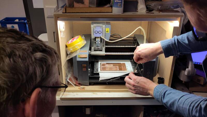
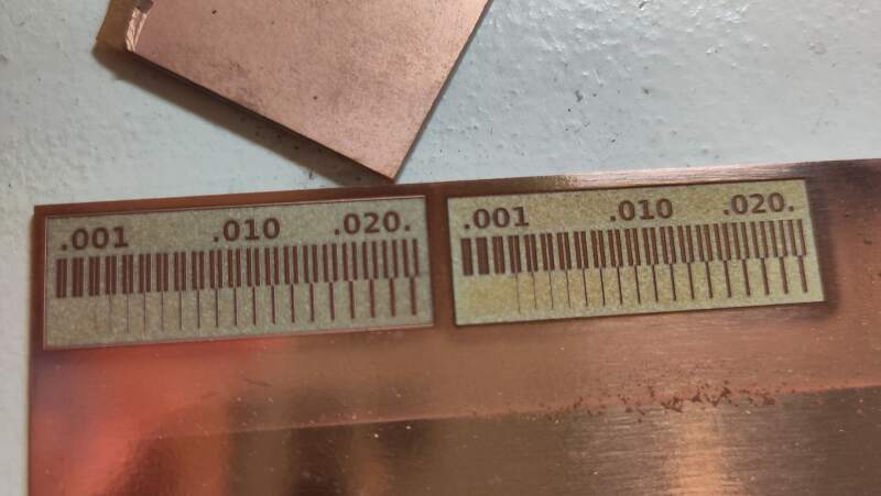
3.1.1. Roland Modela MDX20
Together with Henk, we ran a standard clearance and width test using a 0.4mm flat mill and a tapered mill.
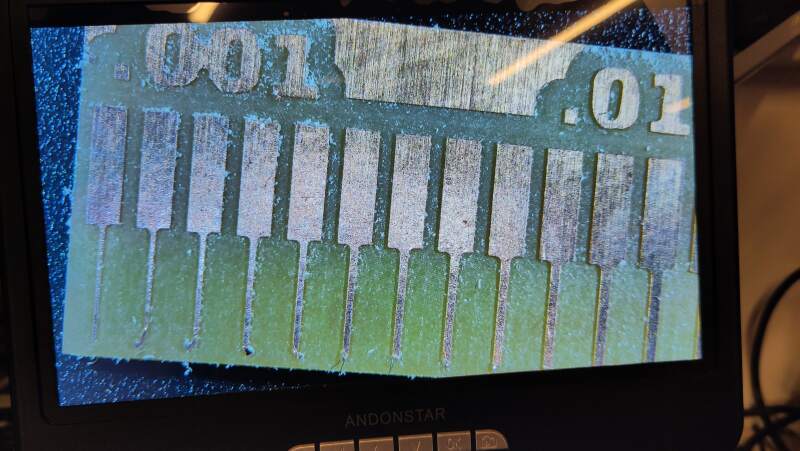
It is obvious that milling will not allow a smaller clearance than the mill bit diameter. On the other hand, it is very impressive how narrow the tracks can be.
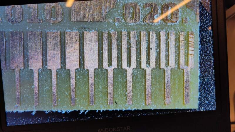
3.1.2. xTool F1 Ultra
The result of running the same test on the laser was very impressive.
3.1.3. Board House
We created an order for the design I made for week 7 at PCBWay (I already have an account there).
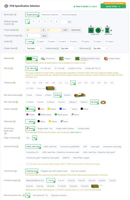
There is a minimum amount of boards is 5. Using the defaults, the cost for the PCBs (without shipping) is 5 dollars. Interestingly 10 boards are the same price, at 15 the price jumps to 15 dollars. The first row of Solder Mask colors are the cheap colors, at the second row the price jumps to 38 dollars.
Another factor in pricing is the Surface Finish, changing that to HASL Lead Free makes it go to 18 dollar but the real money sinks are the gold variants and ENEPIG (Electroless Nickel Electroless Palladium Immersion Gold). According to our local instructor Leo, Immersion Gold (ENIG) is the best value finish. I provides good bonding to solder and is reliable.
We looked at SMD-stencil options but opted to leave it and clicked Save to Card.
Next, we were presented with an upload from for Gerber files.
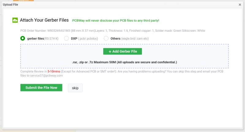
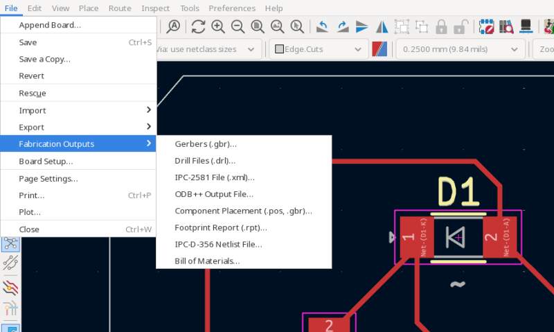
I opened my design in the PCB Editor in KiCad and exported Gerber files.
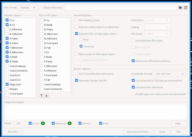
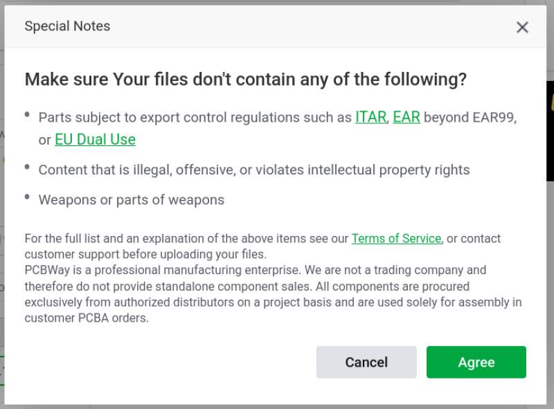
After bundling all files in a ZIP file and uploading it, we had an order in the our shopping cart. However, it was still Subject to audit.
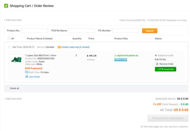
After an hour (or maybe two?), the order was audited and we could Proceed to checkout. But we did not..
3.2. Individual Assignment
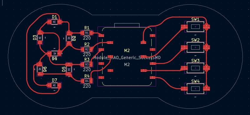
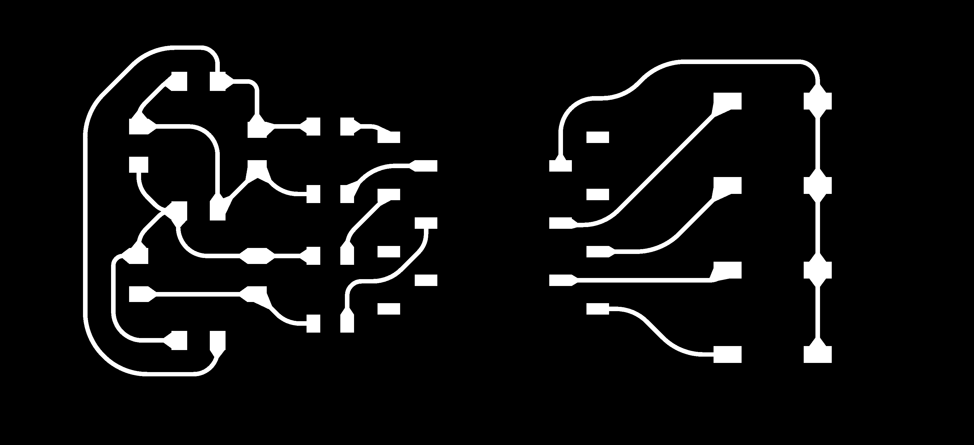
This week I created the board from the Electronics Design week.
3.2.1. Design Rules
I did not change the design rules in the Electronics Design week but after milling with the group, it was obvious we needed to set some boundaries here. From our tests it seemed the Clearance is the most important value to set because the mill is limited in removing copper by the diameter of the bit. Since we are using a 0.4mm flat mill setting the Minimum clearance to 0.4mm is a good first step.
Traces can be a lot narrower because the step size of the machine is much smaller than 0.4mm but just to be safe I opted for 0.4mm as the Minimum track width as well.
My design does not have any holes or other extra features, so I left those values as is.
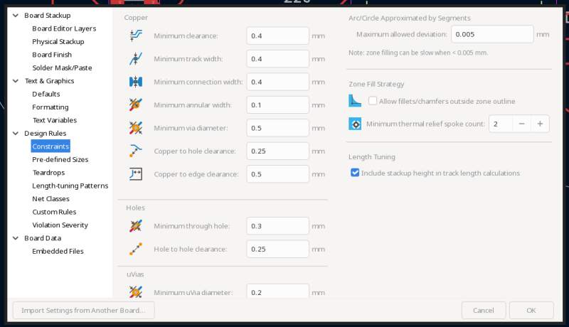
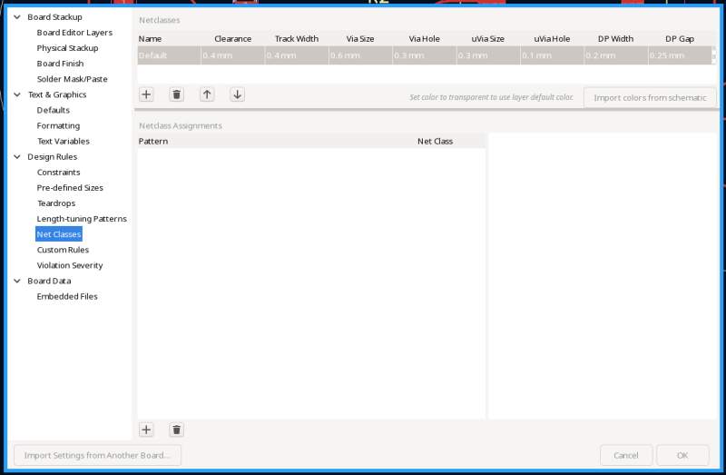
To make drawing these traces easier, I also changed the default Net Class to use a Clearance of 0.4mm and Track Width of 0.4mm.
After setting all this up, I redrew my traces and ran the Design Rules Check with success.
3.2.2. Rounded tracks
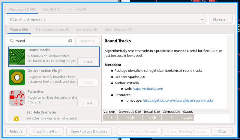
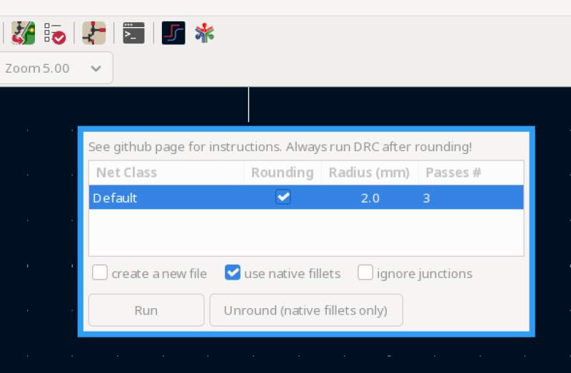
Browsing some of the YouTube channels I subscribe to, I found a video by Mitxela provocatively named: Melt your circuit boards. It describes a KiCad plugin he adopted named round tracks, which rounds the blocky 45° traces in the PCB Editor. I gave it a try, and it looks very nice and friendly.

3.2.3. Something extra
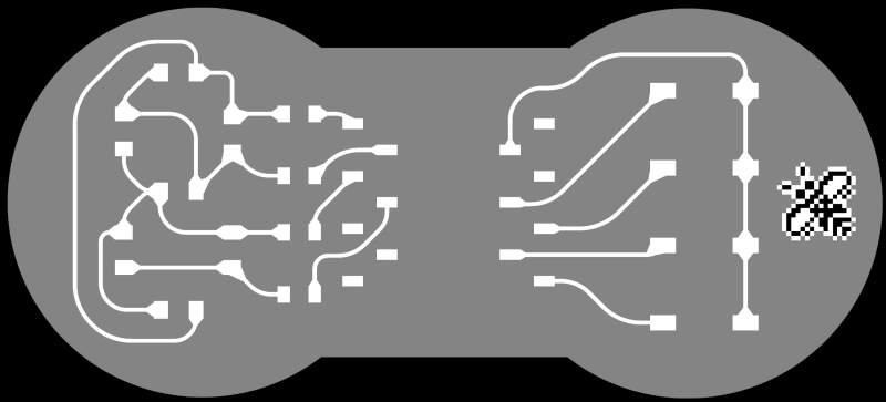
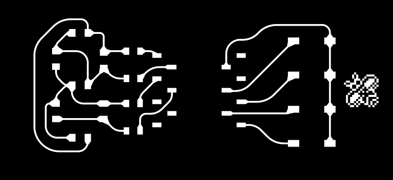
I wanted something extra, so I added the Atari ST busy bee to an unpopulated part of the board, just to see if I could. For this, I exported the board layers to PNG using the Gerber2PNG plugin.
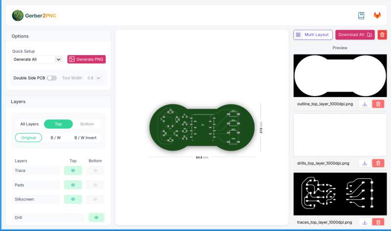
Then, I opened the traces_top_layer_1000dpi.png and outline_top_layer_1000dpi.png in GIMP. I set the outline on top of the traces and set the opacity of the former to 50% (it is only there to see the edge of the board). Then, I added the bee and exported the traces and bee together into a PNG.
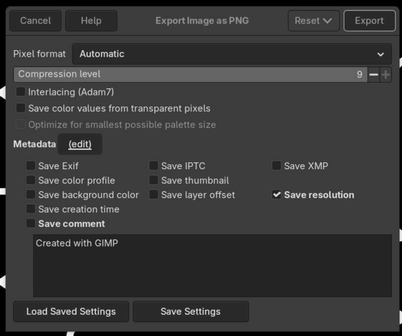
Interestingly the PNG file that GIMP exported was a lot smaller than the original PNG file from the Gerber2PNG plugin; 41KB versus 150KB. I loaded it into mods to see if it was fine and found out I had not exported the resolution (1000DPI) of the PNG file.
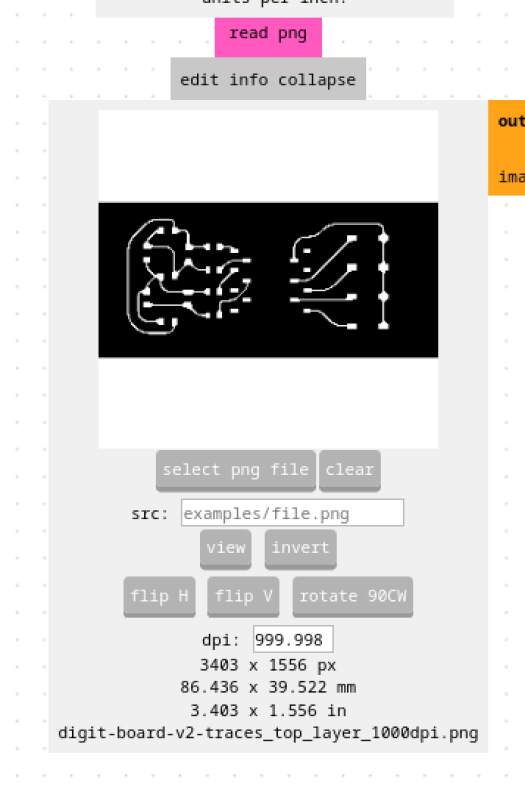
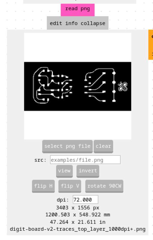
To preserve the resolution in GIMP, tick Save resolution in the export dialog.
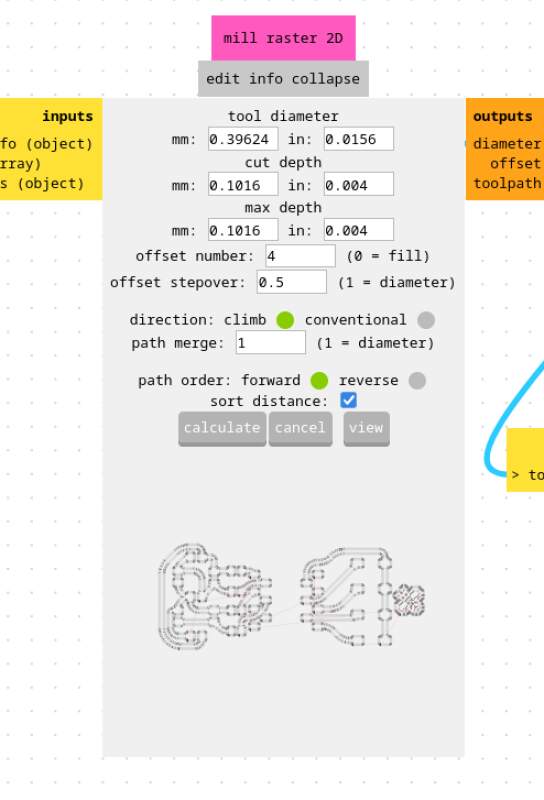
3.2.4. Milling
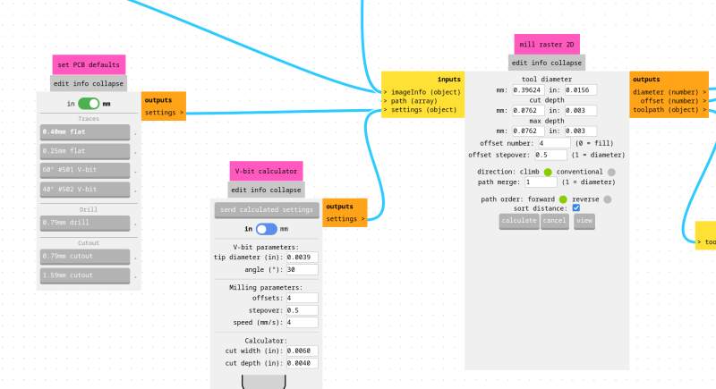
For milling, I used the MDX because I prefer using mods over some software on an MS Windows computer. I used the 0.4mm flat mill as we used in the group assignment, with the settings below:
To get these values, I:
- Selected: 0.40mm flat
- Changed cut depth to: 0.003in
- Changed max depth to: 0.003in
I stuck the board on the sacrificial layer with a couple of small bits of double-sided Scotch tape. A few days, Heleen told me, Henk instructed her to clean the sacrificial layer with sticker remover and cover the entire area with double-sided tape. We all missed this in the instructions, probably because the board we tested on was already fixed to the sacrificial layer. Christian documented this.
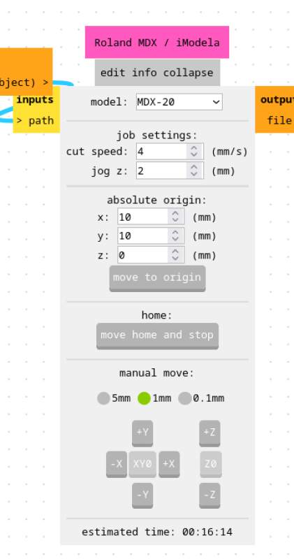
After attaching the board, I selected my modified PNG file and hit Calculate to see the tracks it would make. Next, I did Z-leveling by loosening the mill bit and placing it (gently!) on the copper surface and fastening it. Then, I hit the Move to Origin button. Finally, I clicked Calculate again and Send File. The machine scrawled my traces on the board.
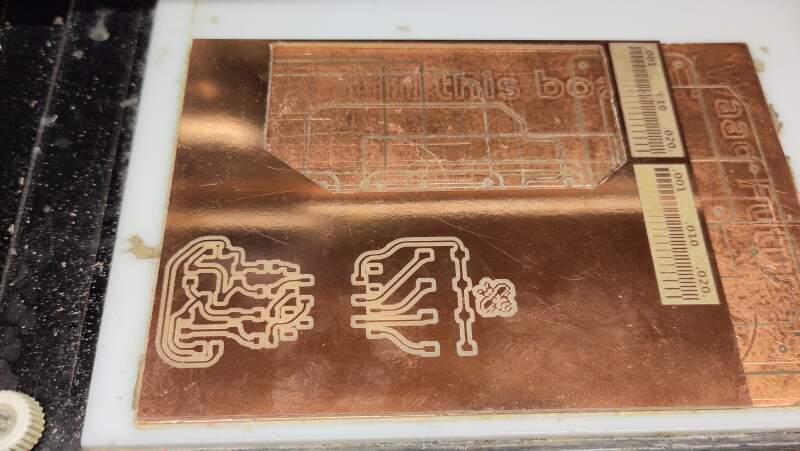
Somehow, I messed up setting the origin properly, and the trace cut was too close to the board edge to get the edge cut I was aiming for (see figure 19). The machine would go back to its zero position, not the one we selected as absolute origin in mods. Heleen had the same problem, and we could not figure it out. After a lot of trial and error, we found out that not using calculate before setting the origin seemed to work.
After milling the traces on a new board using the steps above, I did the same for the edge cut PNG generated by Gerber2PNG. This time, I selected 1.6mm for the max depth to cut through the board. It took a full hour to cut through, compared to 16 minutes for the traces.
A few days later, Heleen told me, I could have set the cut depth to a higher value. Christian documents he used 0.25mm for the edge cut.
For the edge cut I used the following values in mods:
- tool diameter
- 0.4mm
- cut depth
- 0.2mm
- max depth
- 1.65mm
- offset number
- 1
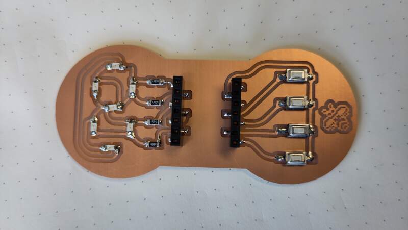
3.2.5. Components
Next up, I needed components to put on the board. To drive LEDs from the RP2040, I added a resistor to protect the microcontroller from burnout. The GPIO can provide 3.3 Volts (or 1.8) when set to output and high. To calculate the resistor value, I used the following formula (found at DigiKey):
\(R = \frac{V_s - V_f}{I_f}\)
To find out forward voltage (\(V_f\)) and forward current (\(I_f\)), I first looked at the link in the fablib entry for the 1206 LED but the DigiKey page states that \(V_f\) varies per color. After consulting Henk, I found the right datasheet via the inventory at fabcloud.io.
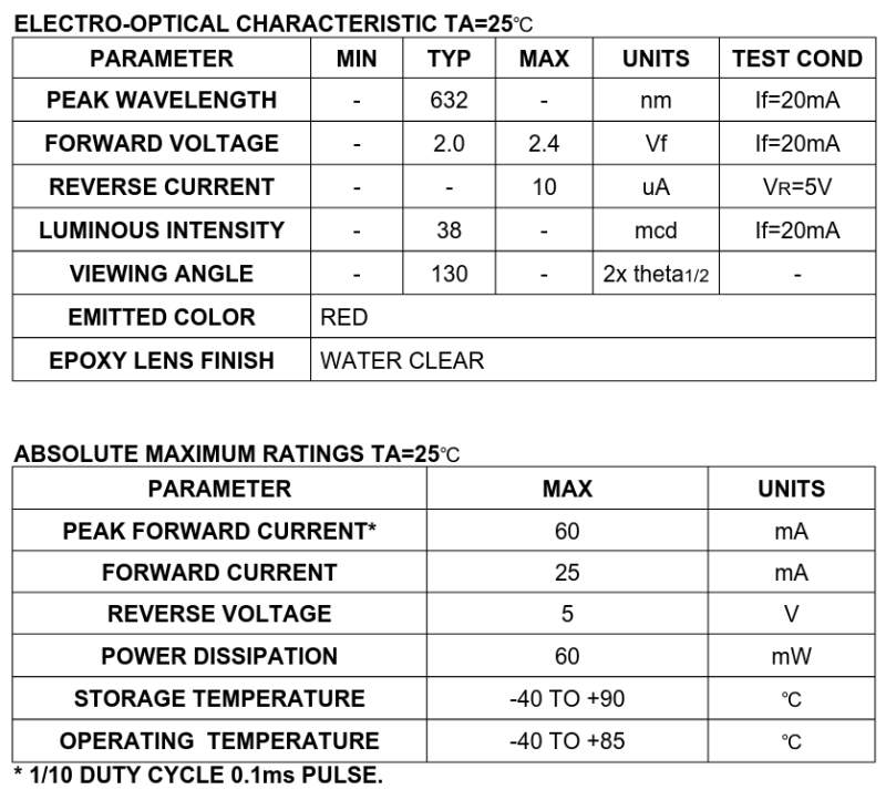
So that makes: \(R = \frac{3.3 - 2.0}{0.025} = 52\) The closes value in the inventor are: 49.9Ω.
| # | Name | Value |
|---|---|---|
| 2 | Female header connectors | 2 pins |
| 2 | Female header connectors | 5 pins |
| 4 | Resistors | 49.9Ω |
| 7 | LED RED CLEAR 1206 SMD | |
| 4 | Push buttons |
3.2.6. Soldering
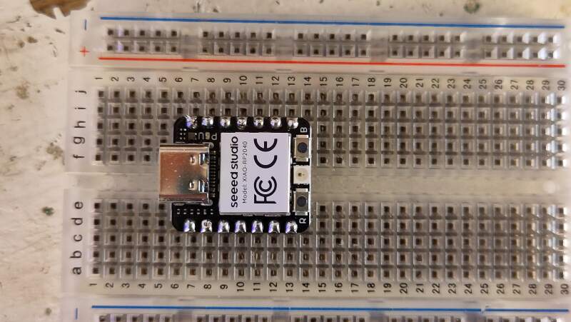
I soldered the header pins for the XIAO using a breadboard.
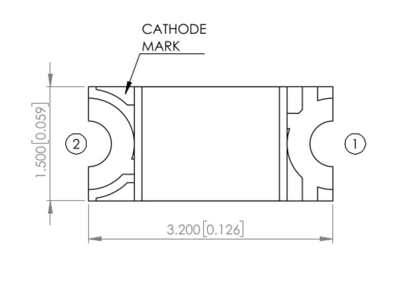
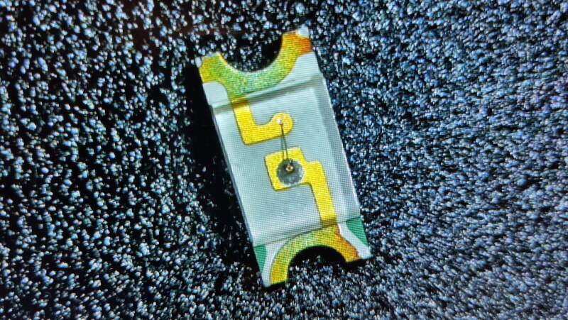
The orientation of the LEDs is very important (the anode should be on the plus side and the cathode on the minus) but they are very small and hard to see which side is which. Fortunately, the LEDs I used have a hint and the datasheet explains it.
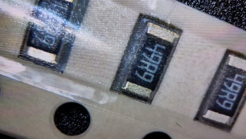
The resistors are also very small and it's very hard to see what value they are. At first, I took some out of the 49.9Ω (49R9) drawer but on further inspection I discovered they were misplaced 4.99Ω (4R99) resistors. I checked the entire box and moved the 4.99Ω in the correct drawer.
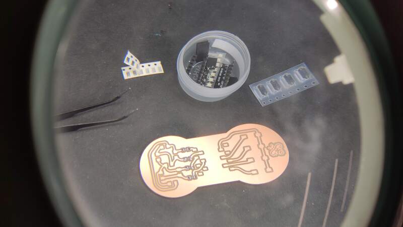
Before soldering I cleaned the board with soap to make the solder bond nicely on the copper. It was impressive how well the solder flowed into the copper.
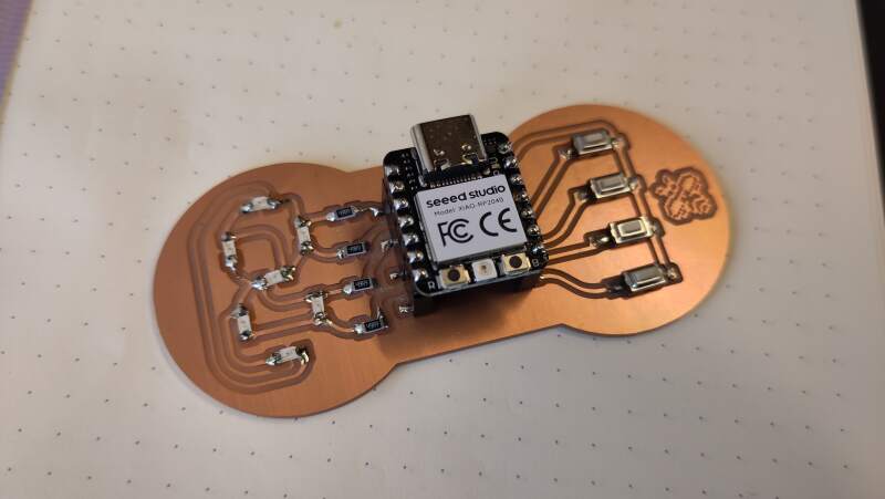
3.2.7. Programming
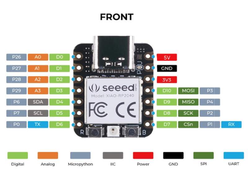
I installed MicroPython on the RP2040 using the UF2 for PICO. Using mpremote I tried to run the LED test script I made week 6, but that did not work because the pin layout on the XIAO is different from the PICO layout, and I wrote the script for a simulation on the PICO.
Here's the adapted script.
import time
from machine import Pin

while True:
    for i in range(26, 30):
        for j in range(26, 30):
            if i != j:
                print(i, "/", j)
                Pin(i, Pin.OUT).value(0)
                Pin(j, Pin.OUT).value(1)
                time.sleep(.5)
                Pin(i, Pin.IN)
                Pin(j, Pin.IN)
And it works! I was very surprised I made no mistakes placing the LEDs.
Blown away by this immediate success, I adapted and tried the counter code from week 4, which also worked. At first, the digits were mirrored, but after swapping the horizontally positioned segments I got that working too.
import time
from machine import Pin

P0=26
P1=27
P2=28
P3=29

A=[P1, P0]
B=[P0, P1]
C=[P3, P2]
D=[P2, P0]
E=[P2, P3]
F=[P2, P1]
G=[P1, P2]

D0=[A, B, C, D, E, F]
D1=[B, C]
D2=[A, B, G, E, D]
D3=[A, B, G, C, D]
D4=[F, B, G, C]
D5=[A, F, G, C, D]
D6=[A, F, G, E, C, D]
D7=[A, B, C]
D8=[A, B, C, D, E, F, G]
D9=[A, F, B, G, C, D]

def show(segs):
    start_time = time.time()
    while time.time() == start_time:
        for seg in segs:
            i = seg[0]
            j = seg[1]
            Pin(i, Pin.OUT).value(0)
            Pin(j, Pin.OUT).value(1)
            Pin(i, Pin.IN)
            Pin(j, Pin.IN)

while True:
    for d in [D0, D1, D2, D3, D4, D5, D6, D7, D8, D9]:
        show(d)
The nice thing is, on Wokwi, it ran too slow to feel like seconds, but on the real thing, it ran at a passable speed. The video below runs in real time.
Since I added push buttons to my design, I wanted to use them too.
Button presses are not detected when simply setting them to Pin.IN.
They need a pull up resistor to detect action on the button. There is
a very nice tutorial about this at SparkFun.
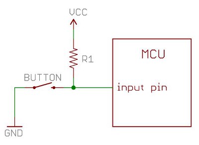
I did not include a resistor in my schematic because the RP2040 has
them built-in on the GPIO pins, and they can be activated by adding
Pin.PULL_UP when setting up the input pins.
Below is the adapted counter code to include actions for the buttons.
import time
from machine import Pin

P0=26
P1=27
P2=28
P3=29

A=[P1, P0]
B=[P0, P1]
C=[P3, P2]
D=[P2, P0]
E=[P2, P3]
F=[P2, P1]
G=[P1, P2]

D0=[A, B, C, D, E, F]
D1=[B, C]
D2=[A, B, G, E, D]
D3=[A, B, G, C, D]
D4=[F, B, G, C]
D5=[A, F, G, C, D]
D6=[A, F, G, E, C, D]
D7=[A, B, C]
D8=[A, B, C, D, E, F, G]
D9=[A, F, B, G, C, D]

def show(segs):
    start_time = time.time()
    while time.time() == start_time:
        for seg in segs:
            i = seg[0]
            j = seg[1]
            Pin(i, Pin.OUT).value(0)
            Pin(j, Pin.OUT).value(1)
            Pin(i, Pin.IN)
            Pin(j, Pin.IN)

B0=Pin(3, Pin.IN, Pin.PULL_UP)
B1=Pin(4, Pin.IN, Pin.PULL_UP) # 3 and 4 are swapped on XIAO
B2=Pin(2, Pin.IN, Pin.PULL_UP)
B3=Pin(1, Pin.IN, Pin.PULL_UP)

DS=[D0, D1, D2, D3, D4, D5, D6, D7, D8, D9]
d = 1
i = 0
while True:
    # second button makes it go backward
    if B1.value() == 0:
        d = -1
    else:
        d = 1

    # third button pauses
    if B2.value() == 1:
        i = (i + d) % len(DS)

    # first button resets to 0
    if B0.value() == 0:
        i = 0

    # bottom button hides digit
    if B3.value() == 1:
        show(DS[i])
    else:
        time.sleep(1)
With the above code loaded, the buttons have the following functions:
- Top button keeps the counter at 0.
- Second button makes it run backwards.
- Third button pauses the counter.
- Bottom button turns the display of the digit off.
4. Reflection
There was little I could prepare at home this week so I adjusted my schedule to allow me to be an extra day in at the Waag. In the end, I did not need the extra day because I only had one small hiccup: the incorrect origin of the traces on the board.
