Electronics Design
1. Week Assignments
Group Assignment:
- Use the test equipment in your lab to observe the operation of a microcontroller circuit board (as a minimum, you should demonstrate the use of a logic analyzer)
- Document your work on the group work page and reflect what you learned on your individual page
Individual assignment:
- Use an EDA tool to design a development board that uses parts from the inventory to interact and communicate with an embedded microcontroller
2. Prior Knowledge
I have never used any of the tools discussed before so I am very excited to get started.
3. Work!
This week we will be playing around with KiCad. I already installed version 9 during the student bootcamp.
3.1. Group Assignment
Here are some photos of the excellent local lecture Erwin gave.

Heleen did an excellent job describing our group efforts this week.
Erwin brought a mystery Arduino Uno which did "stuff" on pins and we were tasked to find out what it does, using the oscilloscope and a logic analyser. It was a fun quest but at some point some of the pins stopped going from high to low. Reconnecting the USB of the board helped so we crashed the firmware! The pins which did not stop flip-flopping were pins with PWN activated so that was an interesting find we could not have made without crashing the software.
We used the following measurement tools:

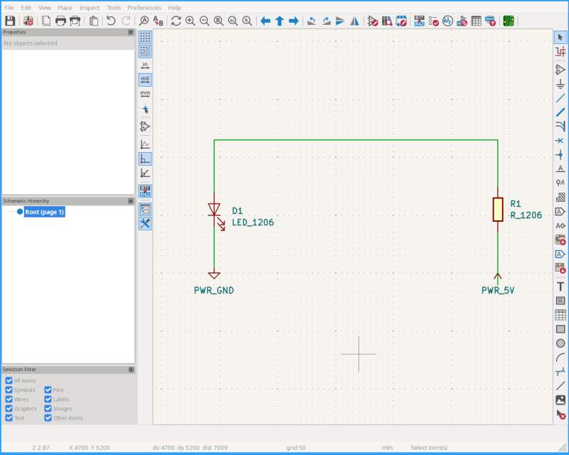
3.2. Simple LED in KiCad
To install the "KiCad FabLib" library in KiCad, I went to Tools -> Plugin and Content Manager -> Libraries, selected the library, used Install and Apply pending changes. It contains the component inventory of the fablabs for use with KiCad.
Then I created a new project in KiCad called "simple-led", opened Preferences and Manage Symbol Libraries. From the Global Libraries list I (only) selected PCM_fab. Next, I opened the Schematic Editor and was presented with a blank canvas.
3.2.1. Schematic
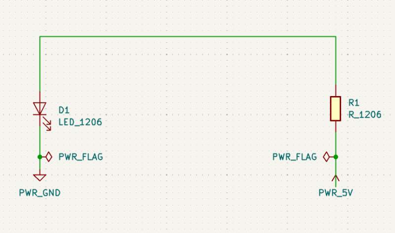
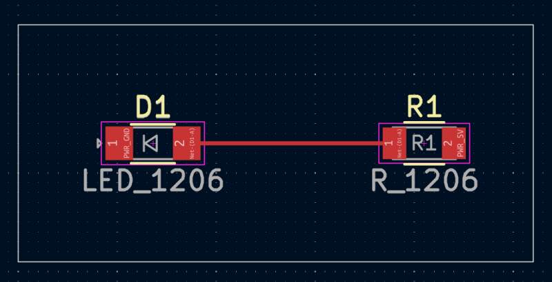
For the first experiment, I want to make a simple circuit to light an LED using an LED and resistor from the "FabLib". I selected the Place Symbols tool, placed a "LED_1206" and a "R_1206" component on the canvas. Then I used Place Power Symbols to add "PWR_GND" and "PWR_5V". With the Draw Wires tool, I connected the LED cathode to ground, the LED anode to the resistor and the other side of the resistor to 5V.
Running the Electric Rules Checker (ERC) gave me two errors about "Input Power pin not driven by any Output Power pins". For "PWR_GND" and "PWR_5V".
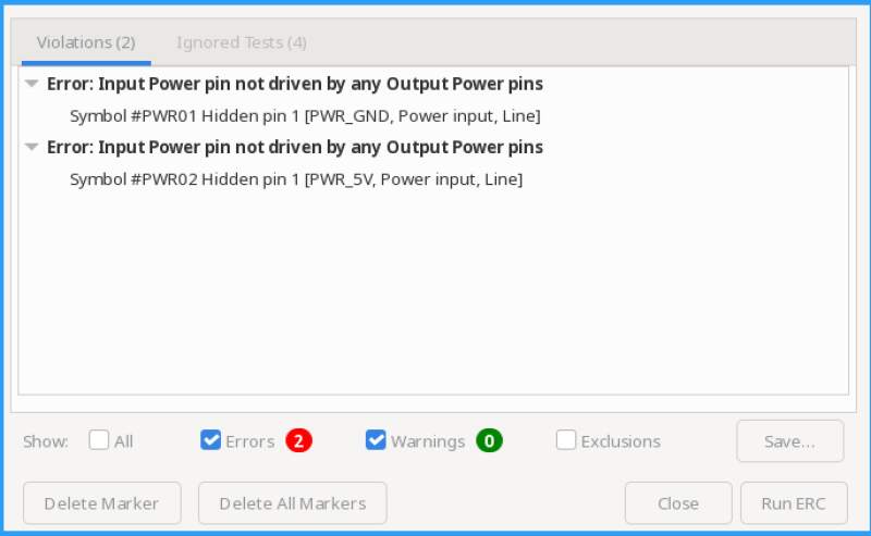
I searched the web and found a KiCad forum post about exactly this issue. Adding "PWR_FLAG" to both wires directly connected to the power symbols fixed the ERC errors. If I understand it correctly, KiCad expects a power source such as a battery or voltage regulator to provide power but no such component is available in the "FabLib".
3.2.2. PCB
Next, I wanted to see what a Printed Circuit Board (PCB) would look like for this circuit. I switched to the PCB editor and ran Update PCB from Schematic.
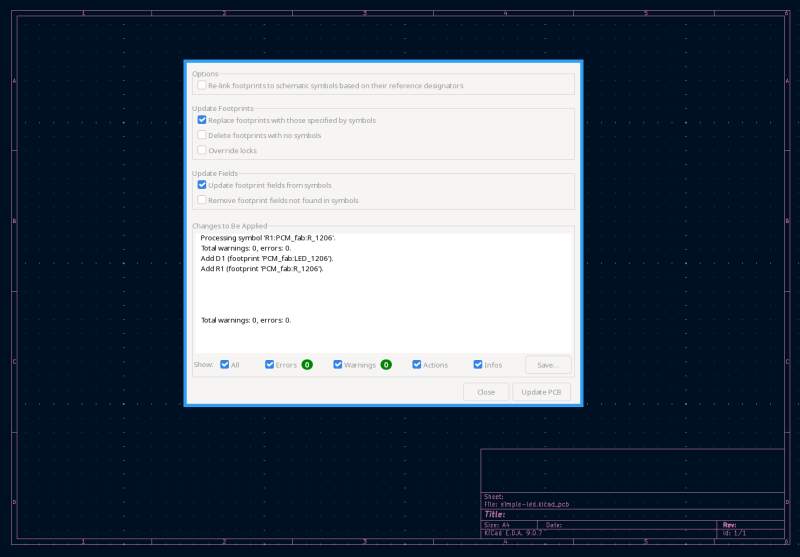
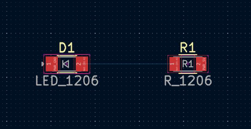
This dropped both components (note, there's no power components here because they are "special" symbols) on the canvas. After placing them next to each other a narrow blue line appeared between them.
Surely the Design Rules Checker (DRC) should fail on this so I ran it. It failed on two errors:
- Violation: "Board has malformed outline (no edges found on Edge.Cuts layer)"
- Unconnected Items: "Missing connection between items"
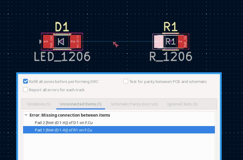
To fix the first issue, I selected the Edge.Cuts layer and used the Draw Rectangle tool to draw a box around the two components. For the second issue I used the Route Single Track tool to draw a trace between the LED and the resistor. Running the DRC yielded no more errors.
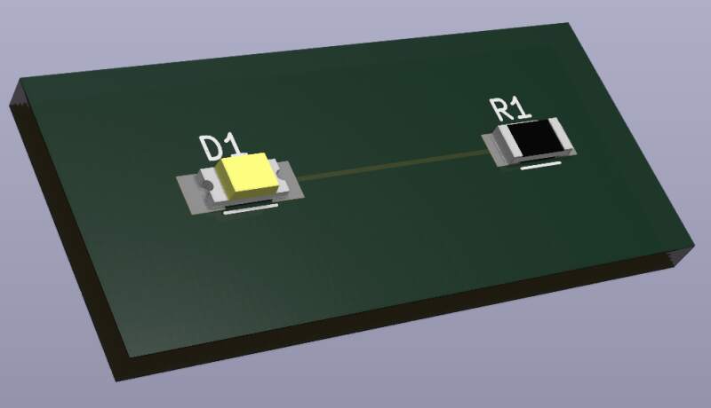
Now, it became very apparent that the power symbols are just some markers. The PCB does not have a way to connect a power source and ground to it. The "FabLib" only contains a coin cell battery holder component, which is an obvious connector for hooking up a battery. I could not find any other connector that is an obvious connector for other power sources. Header pins, perhaps?
3.2.3. Simulation
I noticed KiCad comes with a Simulator tool in the schematic editor, so I just started it to see what happens. It opened a new window with some output on it:
Note: Compatibility modes selected: ps lt a
Line no. 3, d1 __d1, missing tokens
warning, can't find model 'r_1206' from line
r1 net-_d1-a_ pwr_5v r_1206
Circuit: KiCad schematic
Error on line 2 or its substitute:
r1 net-_d1-a_ pwr_5v r_1206
unknown parameter (r_1206)
Command: esave none
It seemed to find my schematic confusing, so I added a value of "100" to "R1" in the schematic editor to make it understand it is a 100Ω resistor. I closed the simulator and reopened it.
Note: Compatibility modes selected: ps lt a
Line no. 3, d1 __d1, missing tokens
Circuit: KiCad schematic
Error on line 3 or its substitute:
d1 __d1
could not find a valid modelname
Command: esave none
That helped for the resistor but it was still confused about "D1", the LED. I opened the properties of the LED in the schematic and found a Simulation Model button which allows me to select a "SPICE model".
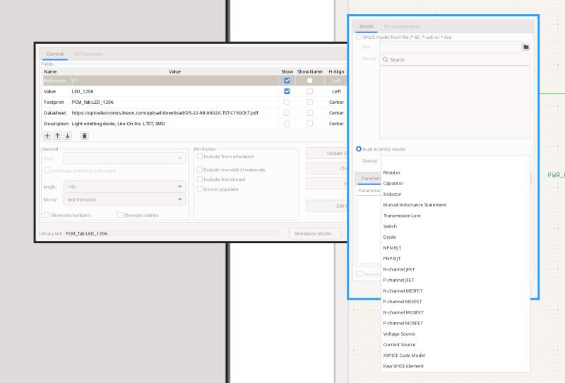
Unfortunately, there's no LED model to select, so I selected Diode because an LED is a diode. I reopened the simulator and the errors were gone.
Note: Compatibility modes selected: ps lt a
Circuit: KiCad schematic
Command: esave none
So I hit "Run Simulation", giving me the following output:
Circuit: KiCad schematic
Doing analysis at TEMP = 27.000000 and TNOM = 27.000000
Using SPARSE 1.3 as Direct Linear Solver
Warning: singular matrix:  check node probe_int_net-_d1-a__r1_1
Note: Starting dynamic gmin stepping
Warning: singular matrix:  check node probe_int_net-_d1-a__r1_1
Warning: Dynamic gmin stepping failed
Note: Starting true gmin stepping
Warning: singular matrix:  check node probe_int_net-_d1-a__r1_1
Warning: singular matrix:  check node probe_int_net-_d1-a__r1_1
Warning: singular matrix:  check node probe_int_net-_d1-a__r1_1
Warning: singular matrix:  check node probe_int_net-_d1-a__r1_1
Warning: True gmin stepping failed
Note: Starting source stepping
Warning: source stepping failed
Note: Transient op started
Note: Transient op finished successfully
 Reference value :  0.00000e+00
No. of Data Rows : 1


Simulation results:

I(r1):                    0A
I(d1):                    -7.8616e-122fA
V(pwr_gnd):               7.8616e-11fV
P(d1):                    -9.58985e-247fW
V(pwr_5v):                -3.9308e-11fV
V(net-_d1-a_):            -3.9308e-11fV
P(r1):                    3.26063e-257fW
Hmm, fA, fV, fW, all femto values; \(10^{-15}\). These values are basically zero…
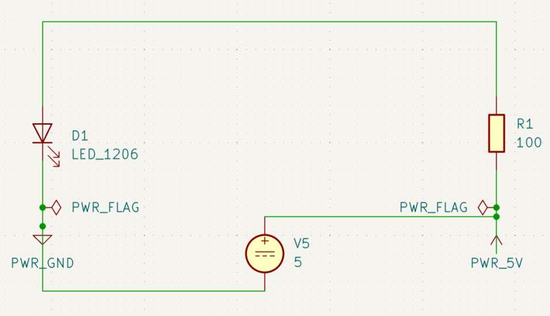
Searching for a solution, I found this KiCad 9 simulation video which adds a special power source for simulations. At that point, I did not have any simulation components available in the component picker. So I went back to the KiCad start window and opened Preferences to open the Manage Symbol Libraries window, found the "Simulation_SPICE" library and activated it. Back in the schematic editor, I could add a "VDC" component from the simulation library and hook it up to the "PWR_GND" and "PWR_5V" parts of the net.
I reran the simulator but the results are not much better:
Simulation results:
I(r1):                    -5.01pA
I(d1):                    -5.01pA
I(v5):                    -5.01pA
P(v5):                    -25.05pW
V(pwr_gnd):               -5V
P(d1):                    25.05pW
V(pwr_5v):                258.016pV
V(net-_d1-a_):            -242.984pV
P(r1):                    2.51001e-06fW
Pico values; \(10^{-12}\)…
I think, the diode needs more simulation model parameters set. I started with Limiting Values.
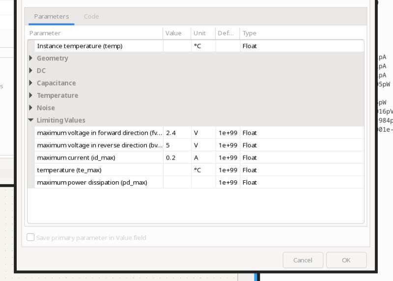
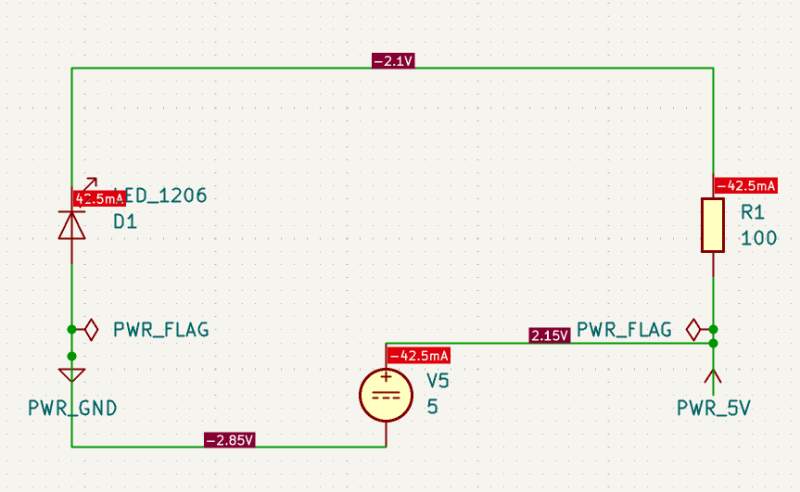
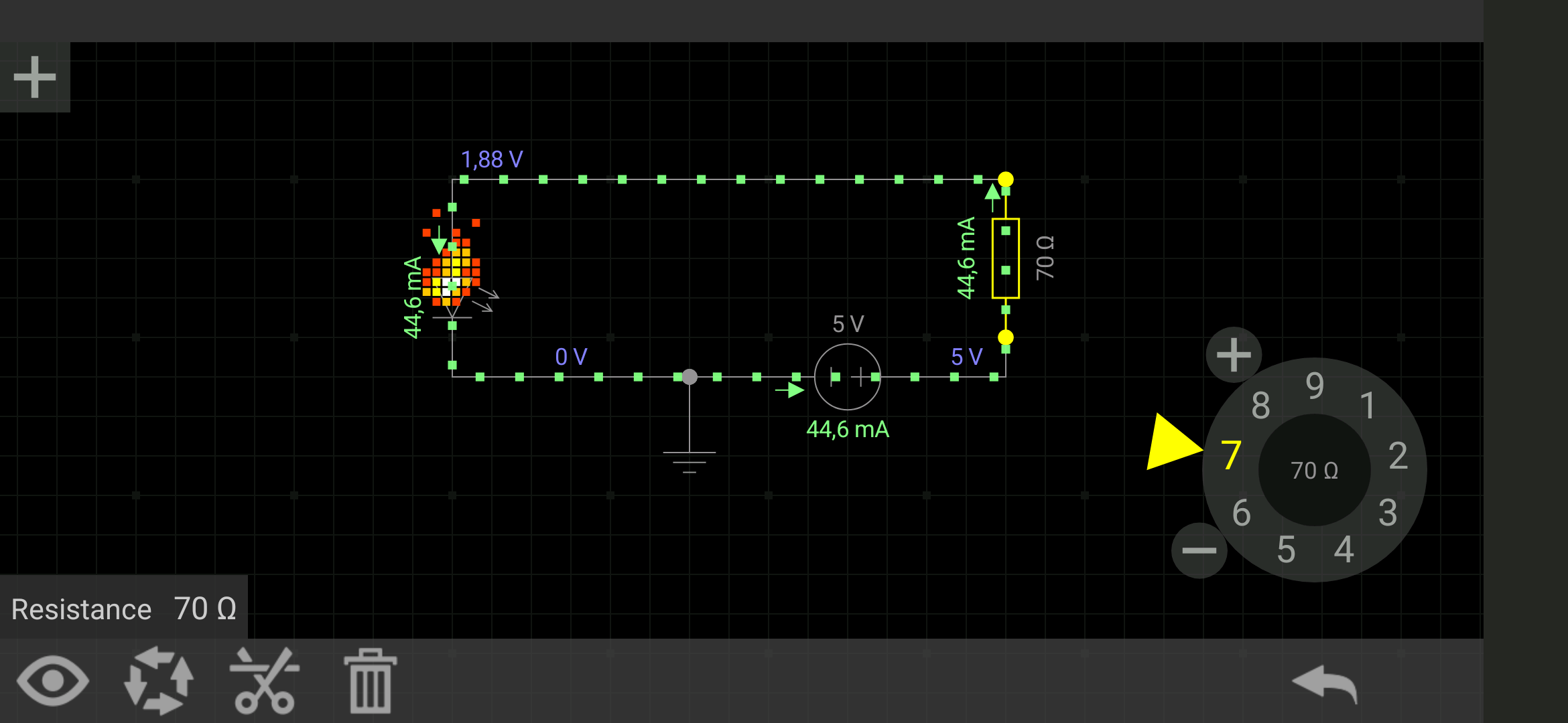
But the values remained the same. Confused, I tried swapping the direction of the LED and the values seemed closer to what I expected.
Simulation results:

I(r1):                    -42.4791mA
I(d1):                    42.4791mA
I(v5):                    -42.4791mA
P(v5):                    -212.396mW
V(pwr_gnd):               -2.85415V
P(d1):                    31.948mW
V(pwr_5v):                2.14585V
V(net-_d1-k_):            -2.10206V
P(r1):                    180.448mW
And they were nicely drawn into the schematic.
I do not know if these values make any sense at all.
The direction of the LED was really bugging me. I opened the Simulation Model for the LED and the anode and the cathode are swapped in the Pin Assignments?!
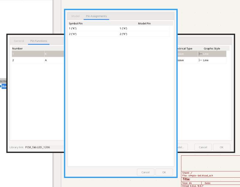
So I swapped them and fixed the schematic. The result became worse.
Circuit: KiCad schematic
Doing analysis at TEMP = 27.000000 and TNOM = 27.000000
Using SPARSE 1.3 as Direct Linear Solver
Warning: singular matrix:  check node probe_int_net-_d1-a__d1_1
Note: Starting dynamic gmin stepping
Warning: singular matrix:  check node probe_int_net-_d1-a__d1_1
Warning: Dynamic gmin stepping failed
Note: Starting true gmin stepping
Warning: singular matrix:  check node probe_int_net-_d1-a__d1_1
Warning: singular matrix:  check node probe_int_net-_d1-a__d1_1
Warning: singular matrix:  check node probe_int_net-_d1-a__d1_1
Warning: singular matrix:  check node probe_int_net-_d1-a__d1_1
Warning: True gmin stepping failed
Note: Starting source stepping
Warning: source stepping failed
Note: Transient op started
Error: Transient op failed, timestep too small
Error: The operating point could not be simulated successfully.
Any of the following steps may fail.!
DC solution failed -
Last Node Voltages
------------------
Node                                   Last Voltage        Previous Iter
----                                   ------------        -------------
probe_int_net-_d1-a__d1_1                      -nan                 -nan
probe_int_probe_int_pwr_gnd_d1_d1_2                 -nan                 -nan
probe_int_pwr_gnd_d1                           -nan                 -nan
d1probe_int_vref                               -nan                 -nan
d1:power                                       -nan                 -nan
net-_d1-a_                                     -nan                 -nan
pwr_gnd                                        -nan                 -nan
probe_int_pwr_5v_v5_1                          -nan                 -nan
probe_int_pwr_gnd_v5_2                         -nan                 -nan
v5probe_int_vref                               -nan                 -nan
v5:power                                       -nan                 -nan
pwr_5v                                         -nan                 -nan
probe_int_net-_d1-a__r1_1                      -nan                 -nan
probe_int_probe_int_pwr_5v_r1_r1_2                 -nan                 -nan
probe_int_pwr_5v_r1                            -nan                 -nan
r1probe_int_vref                               -nan                 -nan
r1:power                                       -nan                 -nan
bprobe_int_r1power#branch                         0                    0
r1:probe_int_n1#branch                         -nan                 -nan
r1:probe_int_n2#branch                         -nan                 -nan
bprobe_int_r1vref#branch                          0                    0
bprobe_int_v5power#branch                         0                    0
v5:probe_int_n1#branch                         -nan                 -nan
v5:probe_int_n2#branch                         -nan                 -nan
bprobe_int_v5vref#branch                          0                    0
bprobe_int_d1power#branch                         0                    0
d1:probe_int_a#branch                          -nan                 -nan
d1:probe_int_c#branch                          -nan                 -nan
bprobe_int_d1vref#branch                          0                    0
r1#branch                                      -nan                 -nan
v5#branch                                      -nan                 -nan
d1#branch                                      -nan                 -nan
doAnalyses: OP:  Timestep too small; trouble with node "d1probe_int_vref"
run simulation(s) aborted

Simulation results:
I'm giving up..
3.3. Simple LED in EveryCircuit
To find out if the values I found in the KiCad simulation (when I swapped the LED) made any sense I, tried EveryCircuit. I recreated the circuit there and ran it.
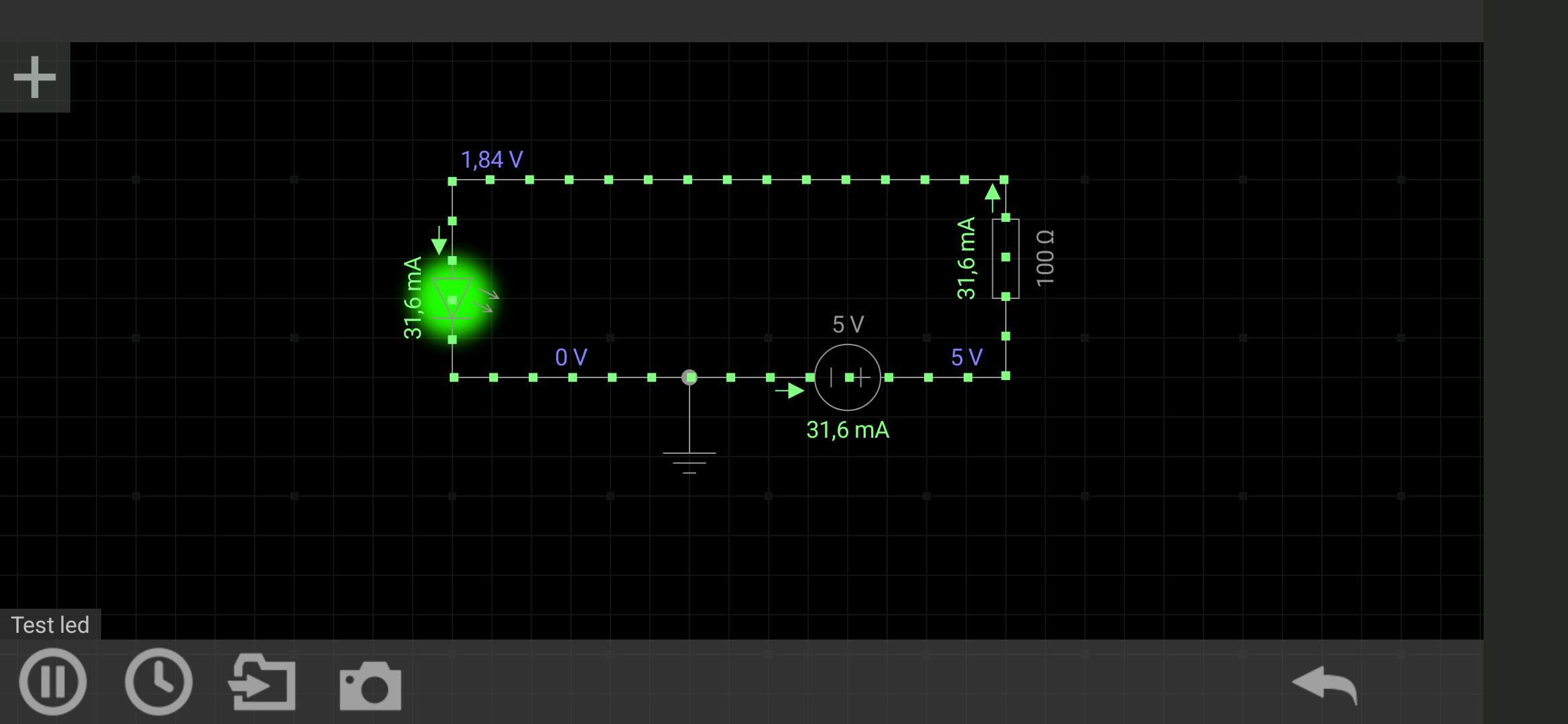
Well, that did not help. I was even more confused now.
A nice thing about EveryCircuit is that it will show a burning component when you over power it.
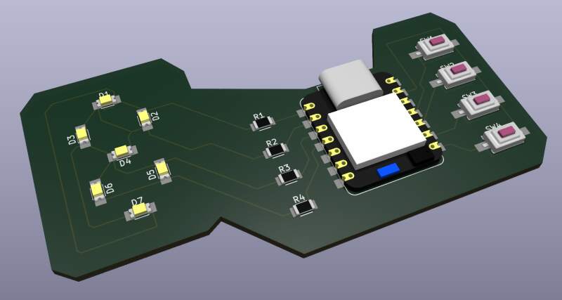
3.4. Clock Board with a Microcontroller
In week 4, I played with the XIAO RP2040, and this week I wanted to make a clock (my final project is an alarm clock) using that microcontroller. The RP2040 contains a Real-Time Clock (RTC), so it should be able to keep time and does not need some extra component to do so. I don't know how I will display time in my final project yet but this week I'll try and see if I can build a 7-segment display digits out of LEDs.
The problem with 7 segment displays is that I need to have \(4 \times 7 = 21\) output pins to drive all LEDs and the XIAO only has 10 I/O pins. I can get rid of one when the left digit only shows 1 or 2 and no 0, but that will not help me much.
Doing a web search, I found out this is, of course, a solved problem. There are specialized chips which can translate a 4-bit (0 till 9 can be encoded in 4 bits) value to a 7-segment output. For instance, the 7447 chip is a "BCD to 7-Segment Decoder". Unfortunately, that still leaves me at \(4 \times 4 = 16\) pins which is still 6 pins over budget.
More web searches reveal that this can be solved by Charlieplexing, which basically only lights up a specific group of LEDs at a specific time but alternates these groups very fast, so the human eye perceives them as all glowing simultaneously. This reminds me of PIO programming on the RP2040, so that should be doable!
As a general rule, using Charlieplexing, one can drive \(n \times (n-1)\) LEDs with \(n\) pins. So, 10 pins can drive \(10 \times 9 = 90\) LEDs! With 6 pins I should be able to drive \(6 \times 5 = 30\) LEDs.
This article about Charlieplexing describes pretty well how to wire these up. So I opened KiCad to write a schematic for this.
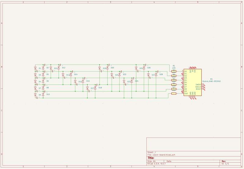
The ERC reported unused pins on the XIAO; I do not know what to do with that.
Next, the PCB! It took me a couple of minutes to realize I had stepped into a horror story. Something I should have realized when making the schematic: plenty of crossing wires!
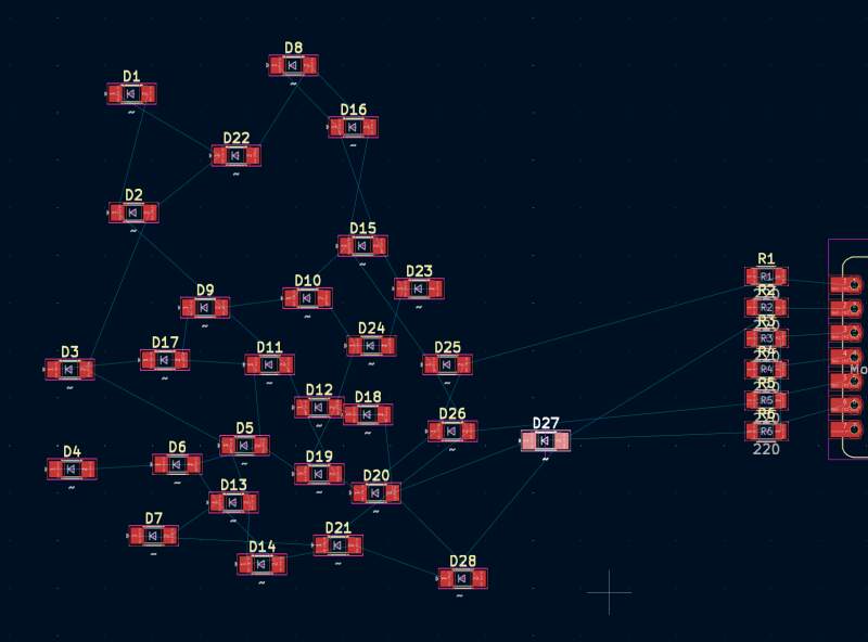
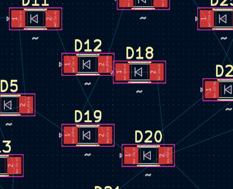
Avoiding crossing wires is going to be hard, and finding an optimal solution (least number of crossing wires) isn't much easier. This goes beyond what I can do this week, so I needed to rethink my design.
3.5. Single digit board
I still liked the idea of Charlieplexing, so I wanted to try and see if a single digit was doable. Having only 7 LEDs means scaling down from 6 pins to 4 pins; which drive \(4 \times 3 = 12\) LEDs.
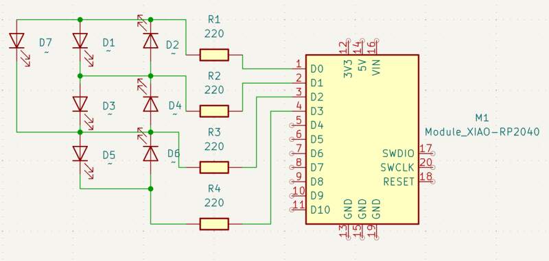
Running the ERC, I am getting plenty of unconnected pin errors because I am not using these pins. I still do not know if and how I need to fix these.
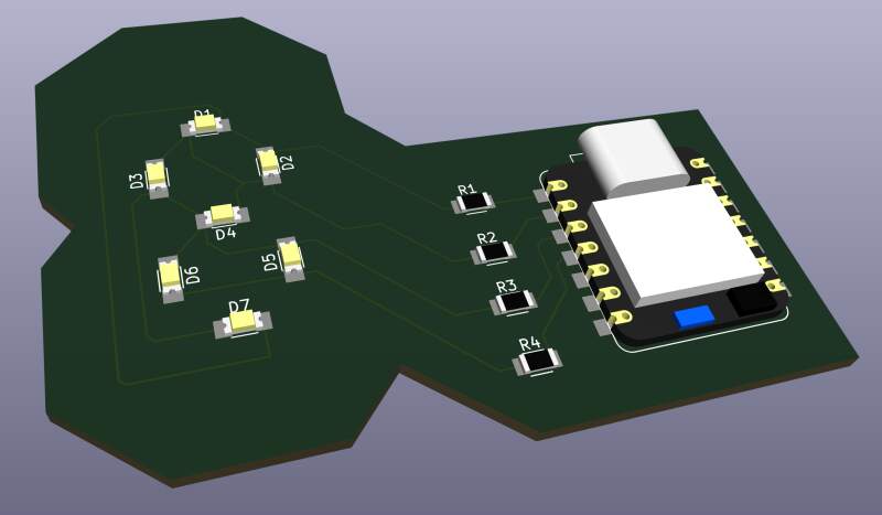
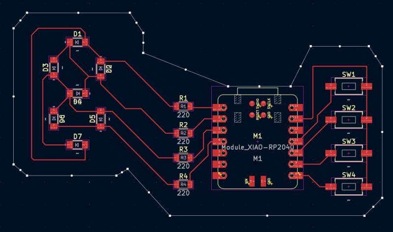
Next, the PCB Editor. This was a lot easier than with 28 LEDs. First, I just spread them out, rotated a few of them to untangle them some more, and moved them around until the routing seemed doable.
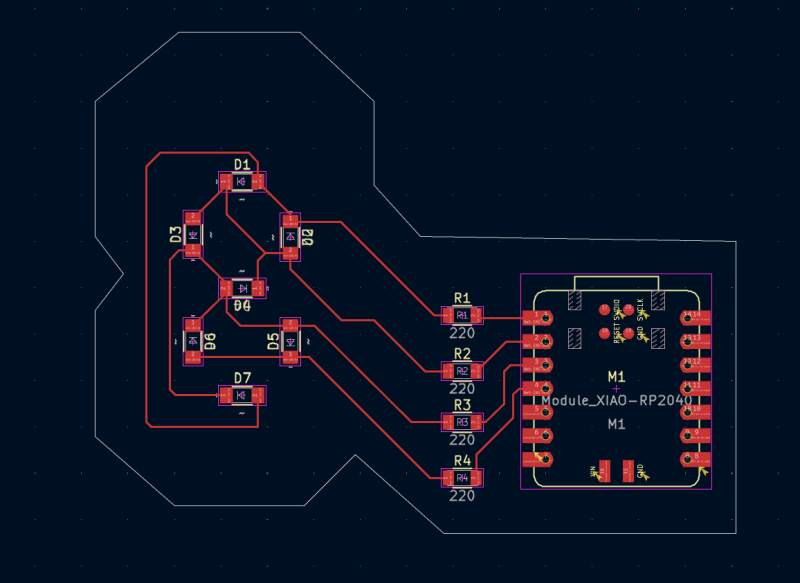
Running the DRC only yielded some warnings about text height being out of range. I think this is because the footprint in the FabLib is incorrect somehow.
3.5.1. Simulation in Wokwi
To see if it actually works, I recreated it in Wokwi. For this, I selected a Raspberry Pi Pico because that's pretty close to a XIAO RP2040; both use an RP2040.
The canvas drawing was a bit hard because the UI does not allow
routing traces but wants to do it for you. This results in wires
drawn on top of each other, making it hard to see which goes where. I
ended up editing the diagram.json JSON-file to hook up the LEDs to
the right resistors. Another advantage of doing this manually was
that I did not see the third pin on the top left of the Pico is a GND
pin and not pin 3. In the JSON file, it is very obvious what is what.
Having all the components in place and hooked up, I translated code from the Charlieplexing website to Python to see if the LEDs could be lit up individually.
import time
from machine import Pin

while True:
    for i in range(4):
        for j in range(4):
            if i != j:
                print(i, "/", j)
                Pin(i, Pin.OUT).value(0)
                Pin(j, Pin.OUT).value(1)
                time.sleep(.5)
                Pin(i, Pin.IN)
                Pin(j, Pin.IN)
And it worked!
Note that sometimes no LEDs are lit at all, that's because only 7 LEDs are present, but 4 pins encode for 12 LEDs, and the code tries all possibilities.
Next, I wanted to make it show digits. First I mapped the LED pin combinations to segments.
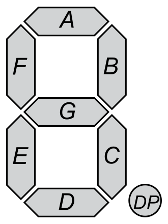
| segment | high | low |
|---|---|---|
| A | 1 | 0 |
| B | 2 | 1 |
| C | 2 | 3 |
| D | 2 | 0 |
| E | 3 | 2 |
| F | 0 | 1 |
| G | 1 | 2 |
I tested this with the code below.
import time
from machine import Pin

A=[1, 0]
B=[2, 1]
C=[2, 3]
D=[2, 0]
E=[3, 2]
F=[0, 1]
G=[1, 2]

while True:
    for p in [A, B, C, D, E, F, G]:
        i = p[0]
        j = p[1]
        Pin(i, Pin.OUT).value(0)
        Pin(j, Pin.OUT).value(1)
        time.sleep(.5)
        Pin(i, Pin.IN)
        Pin(j, Pin.IN)
With the above, I tried to make digits.
import time
from machine import Pin

A=[1, 0]
B=[2, 1]
C=[2, 3]
D=[2, 0]
E=[3, 2]
F=[0, 1]
G=[1, 2]

D0=[A, B, C, D, E, F]
D1=[B, C]
D2=[A, B, G, E, D]
D3=[A, B, G, C, D]
D4=[F, B, G, C]
D5=[A, F, G, C, D]
D6=[A, F, G, E, C, D]
D7=[A, B, C]
D8=[A, B, C, D, E, F, G]
D9=[A, F, B, G, C, D]

def show(segs):
    start_time = time.time()
    while time.time() == start_time:
        for seg in segs:
            i = seg[0]
            j = seg[1]
            Pin(i, Pin.OUT).value(0)
            Pin(j, Pin.OUT).value(1)
            Pin(i, Pin.IN)
            Pin(j, Pin.IN)

while True:
    for d in [D0, D1, D2, D3, D4, D5, D6, D7, D8, D9]:
        show(d)
The result is very slow but it works! To get this to run properly, I'll need to play around with PIO. The following video run at 10 times speed.
3.5.2. Some push buttons
Because Charlieplexing saved me some pins, I decided to add some push buttons to the board to allow adding some functionality using software. Directly driving 7 LEDs and 4 push buttons would have been impossible without Charlieplexing on the XIAO because it only exposes 11 I/O pins!
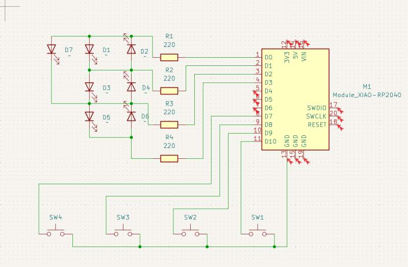
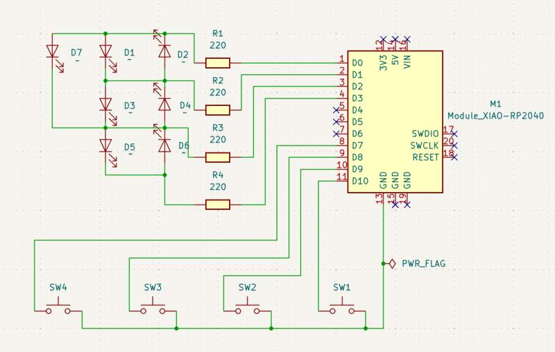
The ERC errors are really annoying, especially the one about pin 13, which I am using for ground for the push buttons. Do I need a "PWR_FLAG" here?
[power_pin_not_driven]: Input Power pin not driven by any Output Power pins
    ; error
    @(8400 mils, 3450 mils): Symbol M1 Pin 13 [GND, Power input, Line]
For all the errors, see: ERC.rpt.
Back at the Waag I asked Henk about these ERC error and my dear peer Christian told me the solution: use the Place No Connection Flags tool to mark the unconnect pins and add a "PWR_FLAG" to get around the error on the ground pin.
4. Reflection
What a ride! I was really looking forward to this week and it totally delivered.
4.1. Good
4.2. Bad
4.3. Ugly
The final board is ugly. I created the edge cut very fast to satisfy the DRC but wanted to try make something prettier in Inkscape an import that. Next time, I'll add a edge cut before doing the routing because moving components breaks the routing.
Also, I don't understand simulation in KiCad, and that's probably why it was not covered in the lectures because it is an advanced feature.
5. Source Files
KiCad projects:
Wokwi digit board:
