After the previous week of designing our boards we come back to manufacturing our boards, bringing our designs to life
This week started slow with fixing some errors in the file
.Group assignment.
What is a pcb?
A Printed Circuit Board (PCB) is a flat board made of insulating material (like fiberglass) with conductive copper tracks that connect different electronic components. Instead of using traditional wiring, a PCB provides a structured layout for electrical connections, making circuits more compact, reliable, and easier to manufactu
Vital pcb parts
Substrate (Base Material): Usually made of FR4 (fiberglass-reinforced epoxy resin) for strength and durability.
Copper Layer: Thin layers of copper act as electrical pathways connecting components
Solder Mask: A protective layer that prevents short circuits and oxidation of copper traces.
Silkscreen: Printed labels on the PCB surface that indicate component placement and reference designators.
Types of pcb -
Single-layer PCB: Has a single copper layer, used in simple circuits.
Double-layer PCB: Copper traces on both sides, allowing more complex designs.
Multilayer PCB: Multiple stacked layers, used in advanced applications like computers and communication devices.
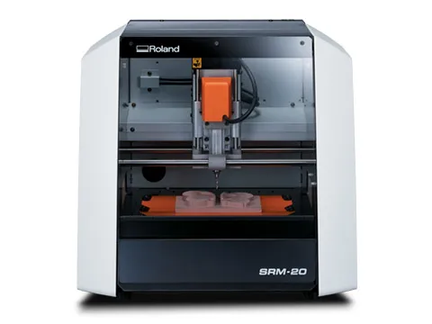
Understanding the machine
Our riidl fabLab has th Roland SRM-20 machine
This is an enclosed milling machine with a bed size of 15 cm by 20 cm
If you want to mill larger PCB's we also have the Protomat E44
The machine supports single- and double-sided PCBs and is ideal for small-scale production, research labs, and educational purposes.
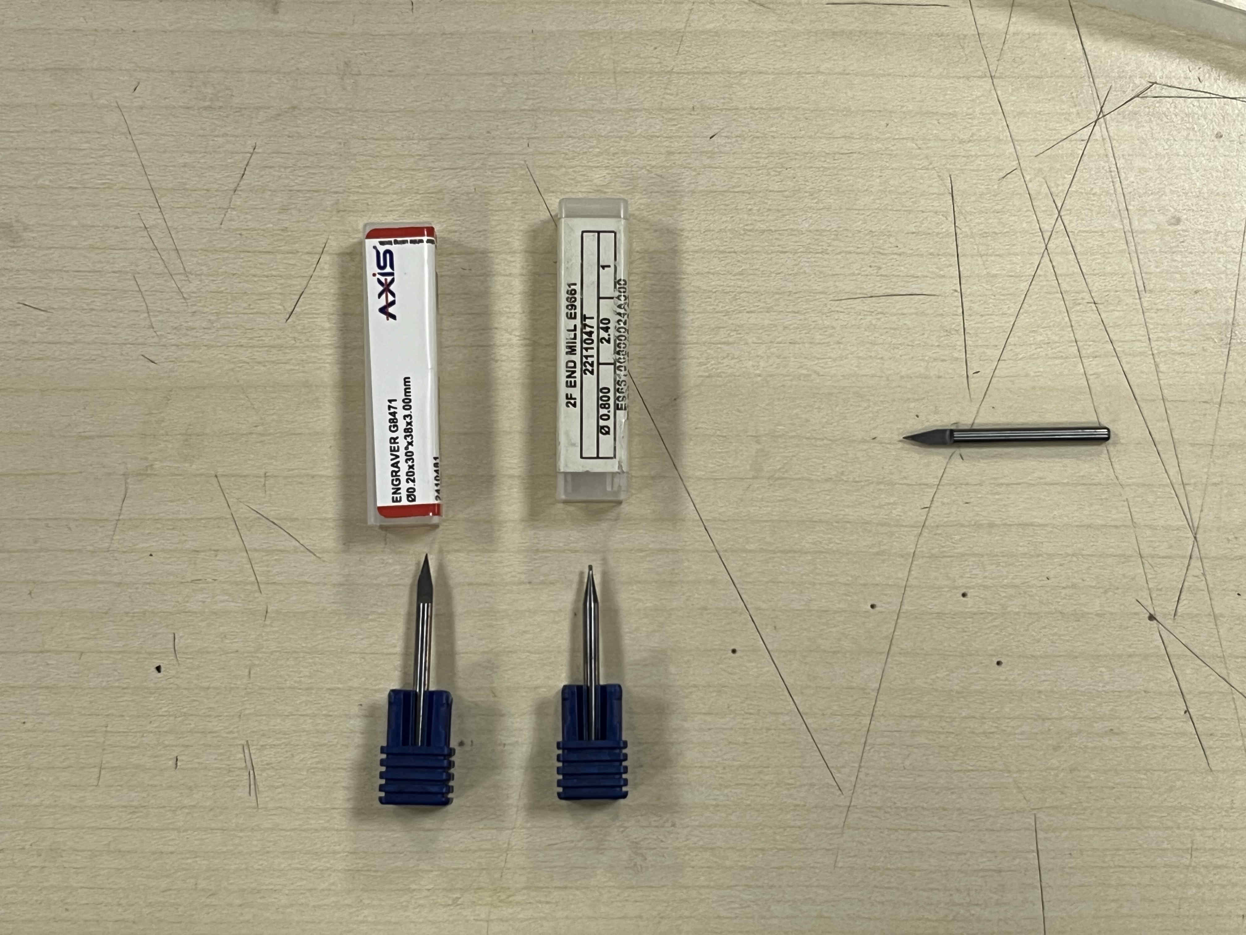
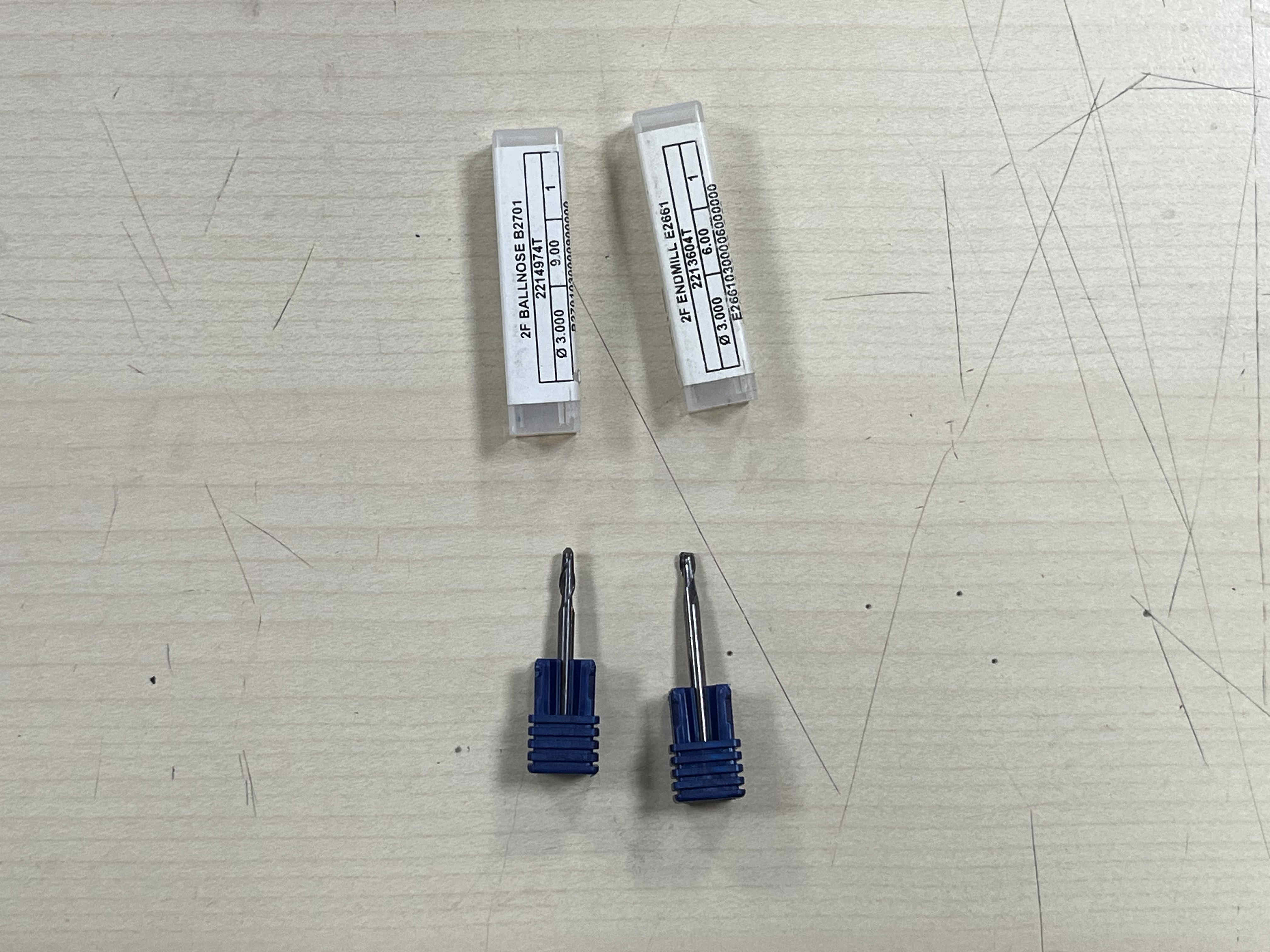
Understanding cutting bits
Our srm-20 can be used to mill and etch copper pcb's one layer at a time and also industrial wax blocks
DIfferent bits are used for different operations of making finished PCB's and wax mother molds
These are the bits used for etching and drilling PCB
The on on the left is v taper 0.2 mm etching bit, and the one on the right is a drill bit for via's and mount holes
Similarly these are the drill bits for creating wax moulds
The on on the right is a flat endmill, for larger step operations, once done, The one on the left, a ball nose end mill is used to smoothen out rough contour curves
Softwares
The tech stack you will need to make PCB's is as such-
EasyEDA/eagle/KiKad - For designing schematic and PCB, and then exporting a Gerber file
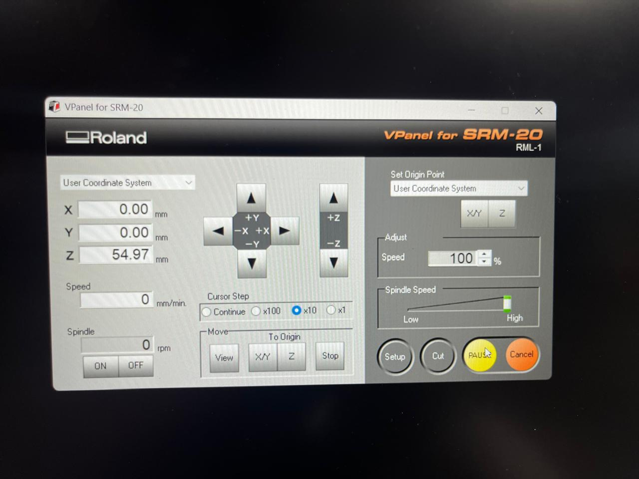
V-panel(in our case) - To set origin and operarting the SRM-20 through desktop
CopperCam - To create operation G-code type file to mill out the required from the Machine
Context
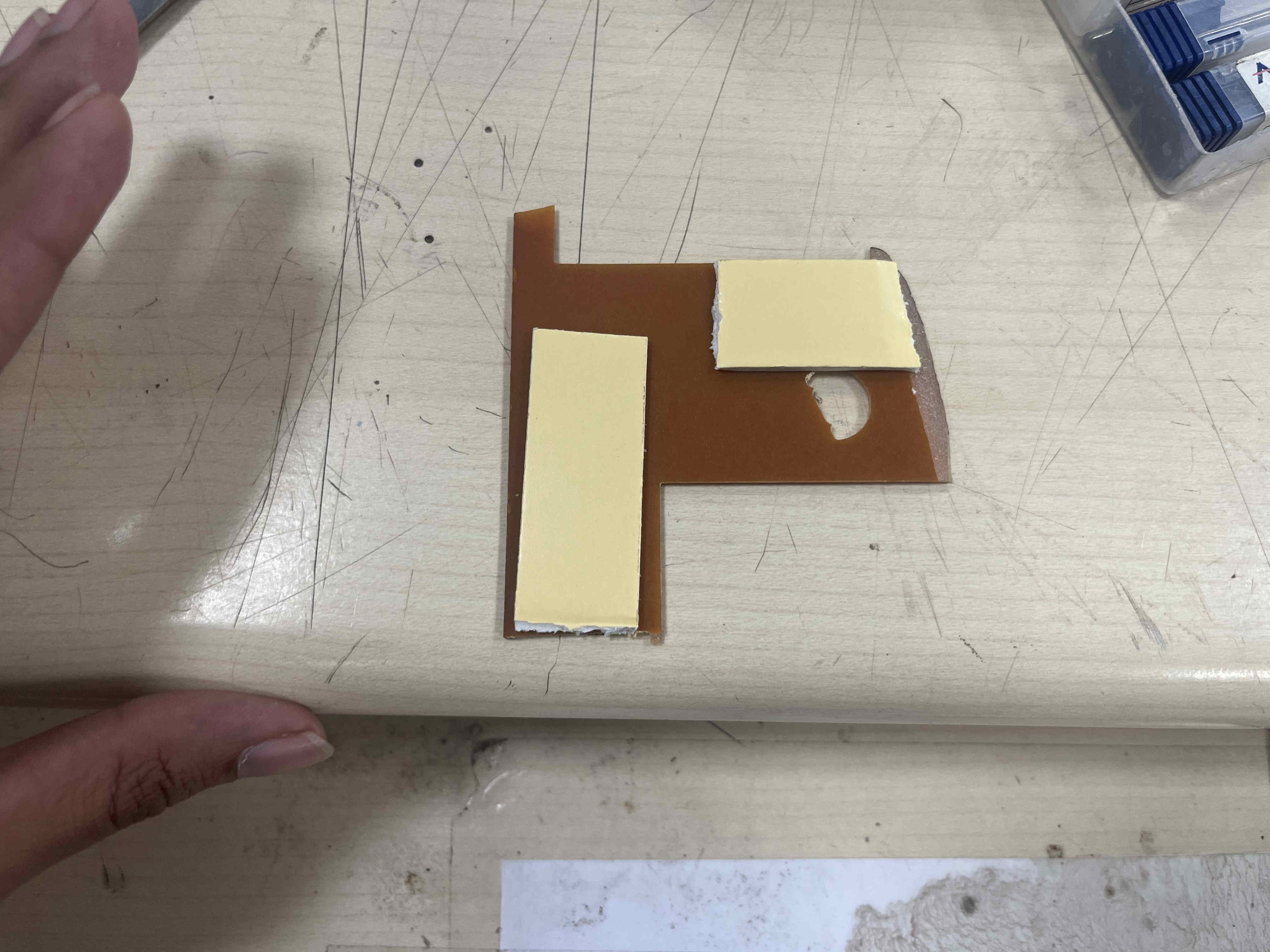
So I had a very specific design which i needed to execute for this week and electronics design week
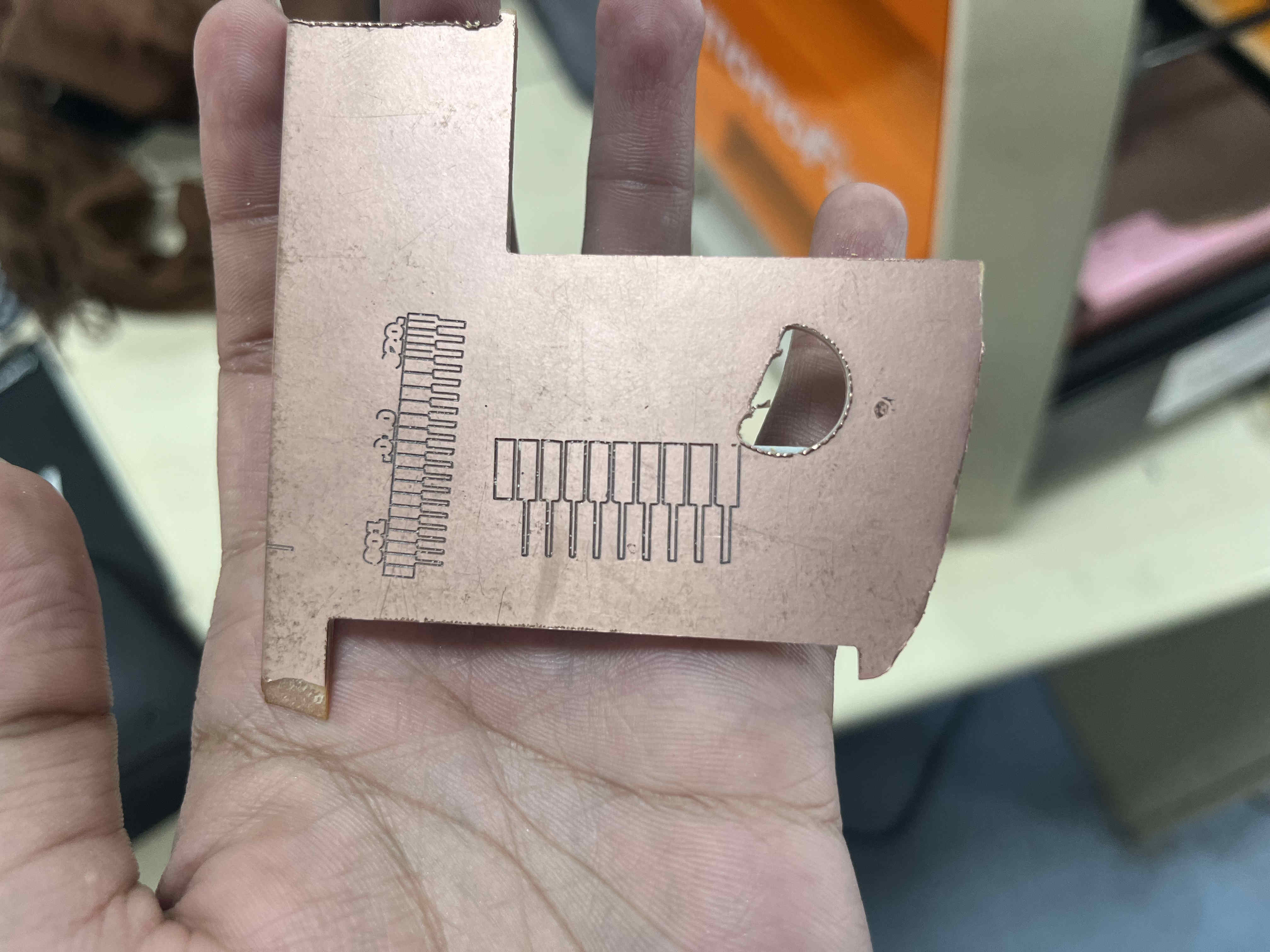
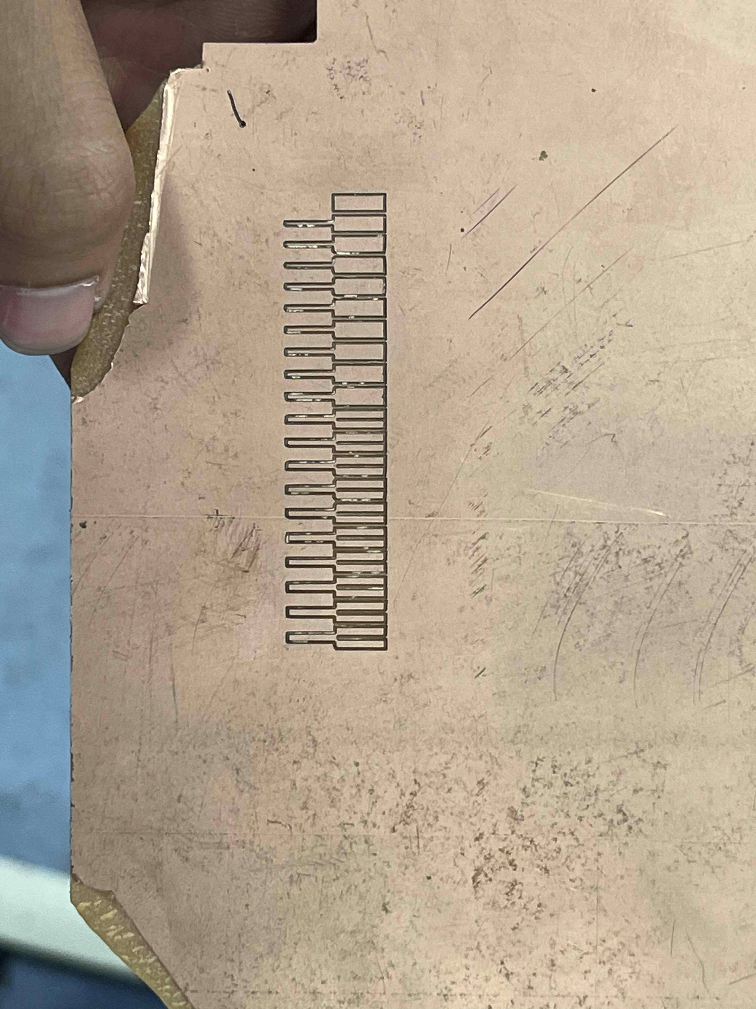
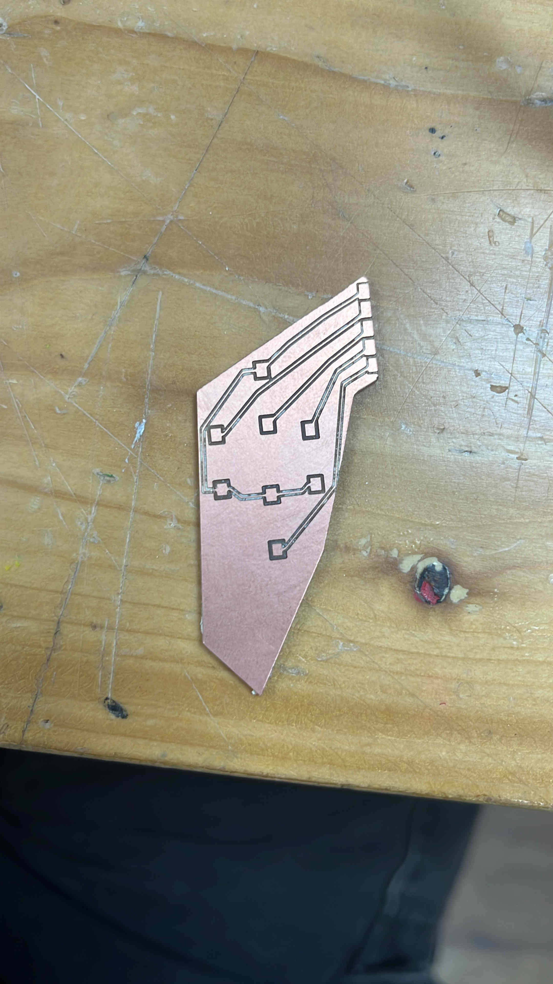
its one of my older design projects that features a BENT body
Now you know why my pcb looks weird xD
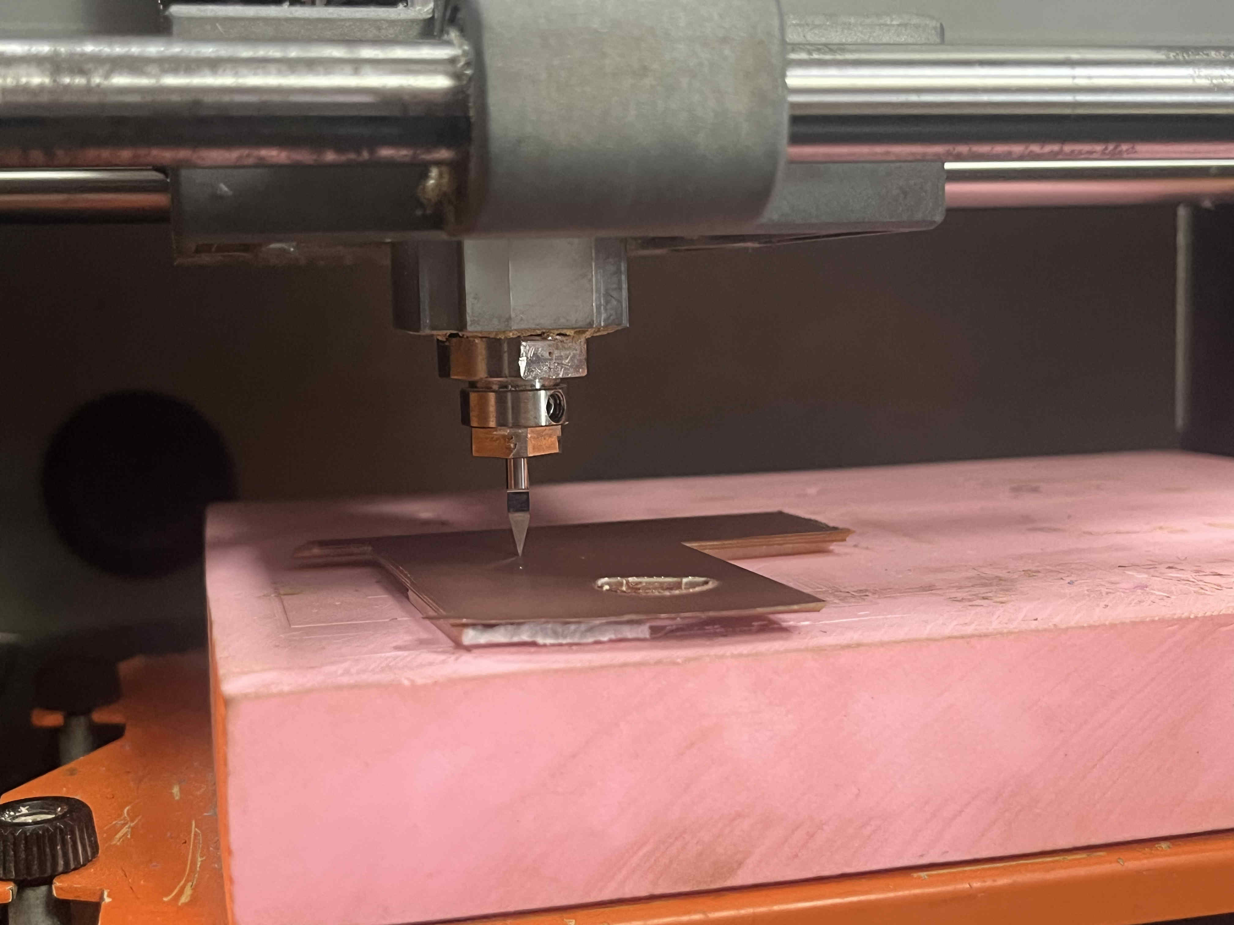
.Testin
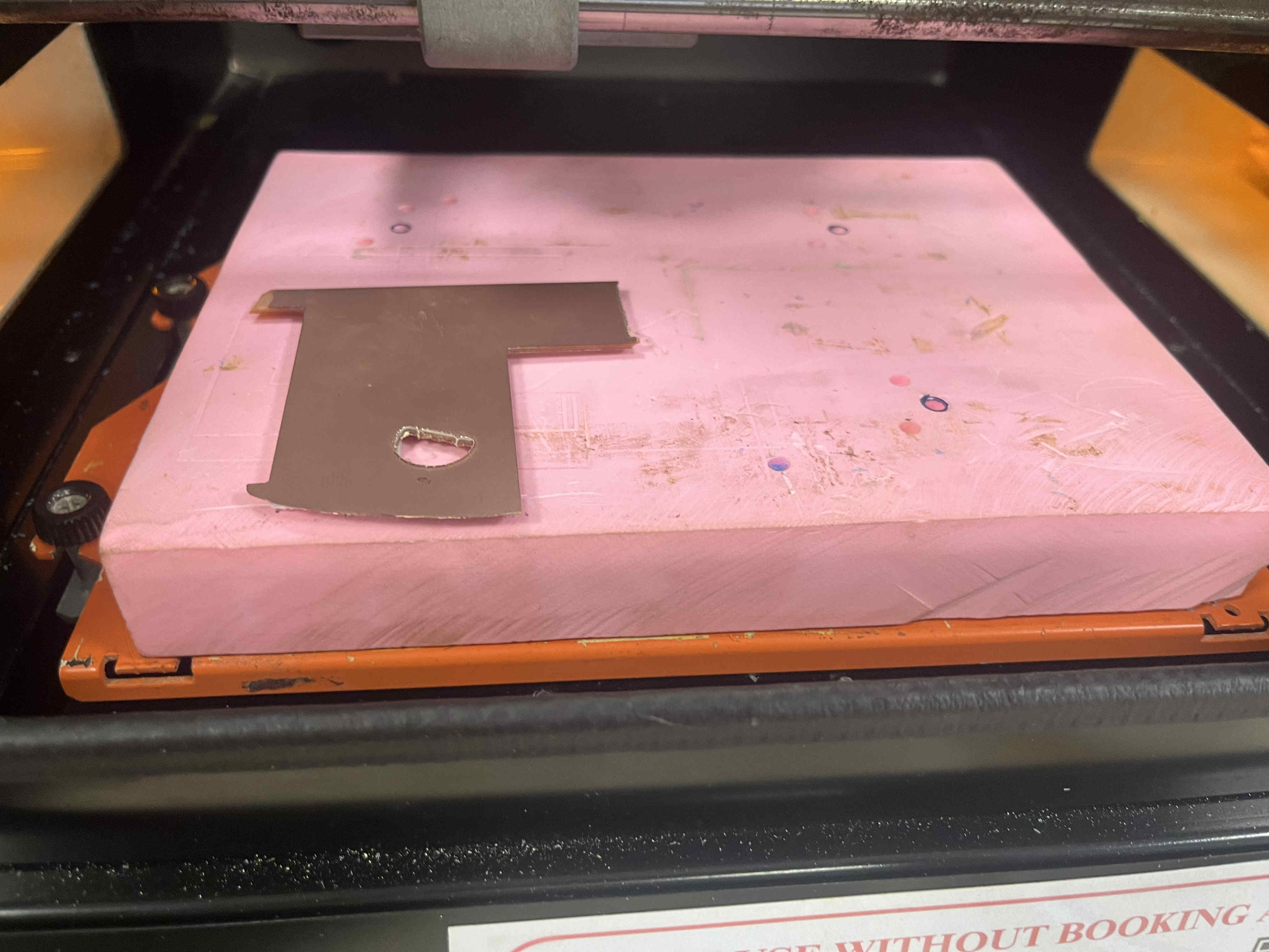
Add double side tape on your clad
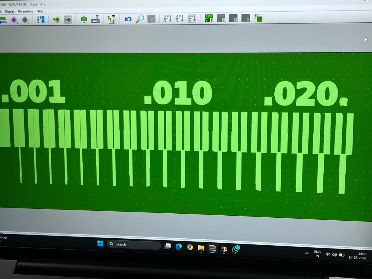
This is a used piece for test file
Stick it firmly
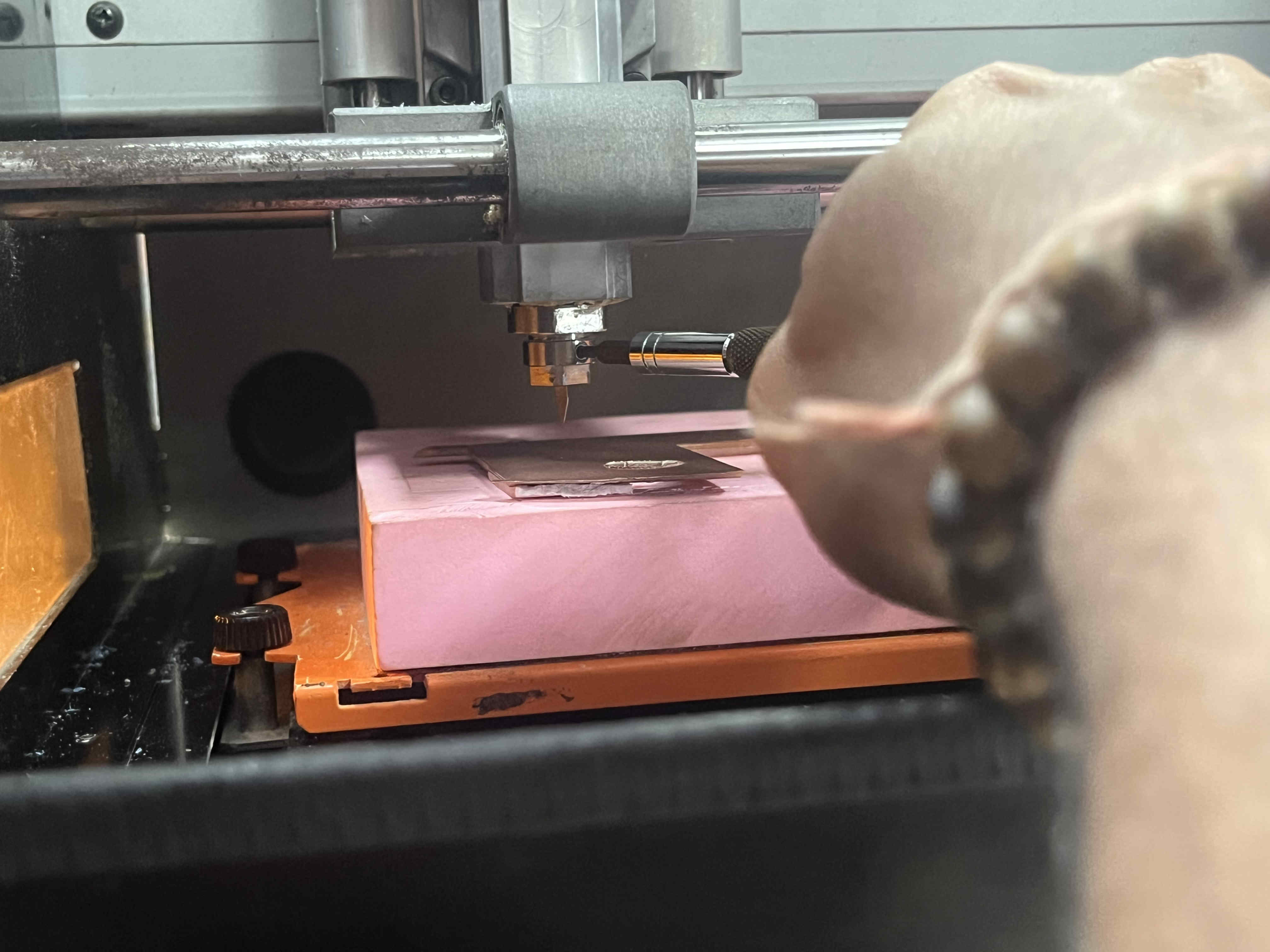
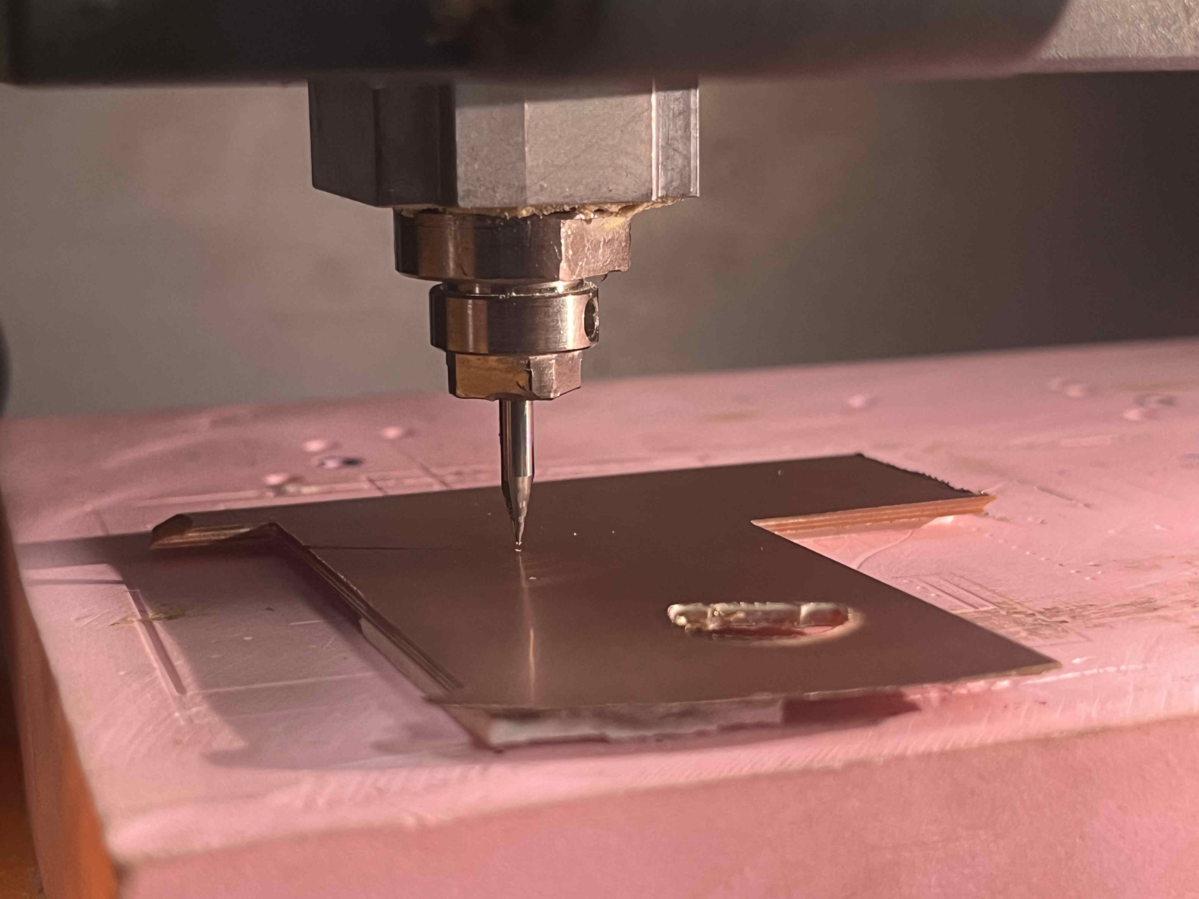
Z axis levelling
First we take our bit and insert it all the way in.
Tighten the screw
Bring z axis down such that theplate does not touch
Then loosen the bit and let the drill bit drop on the plate
Retighten the bit while putting slight pressure on the plate while holdind the bit
You are good to go.To create the file, open easy eda and make a new pcb and upload the test SVG
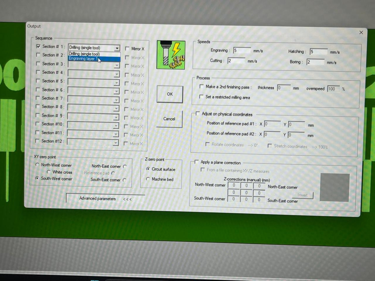
For our machine, this is the controller, called V-PANELopen your file on coppercam.
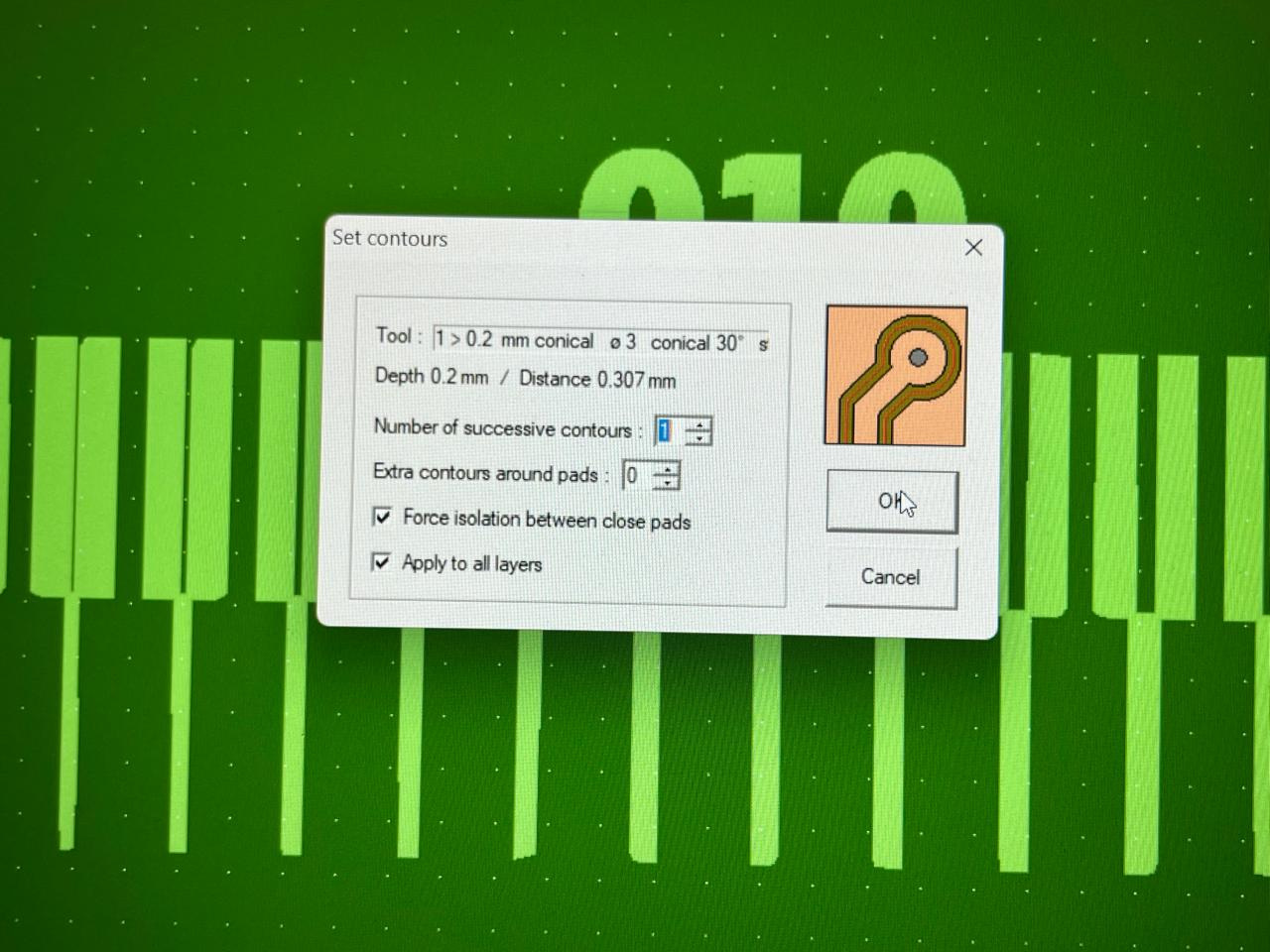
It will most likely be a GTL file named TOP layer
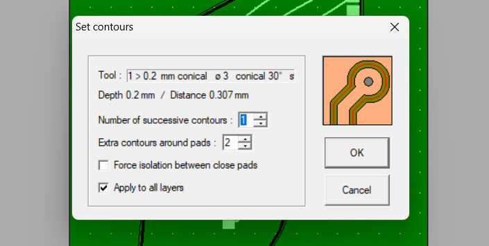
Set contours to 1 and extra contours to 1 or 2 more than the contour
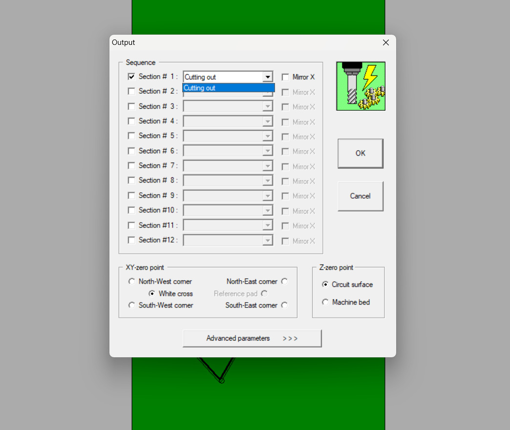
A contour preview should appearSome are red but thats expected as the test file will fail in some regions, tweak contours till most regions passClick the mill option.add sections and select the engraving layerSet origin according to v-panel placement
Click okay
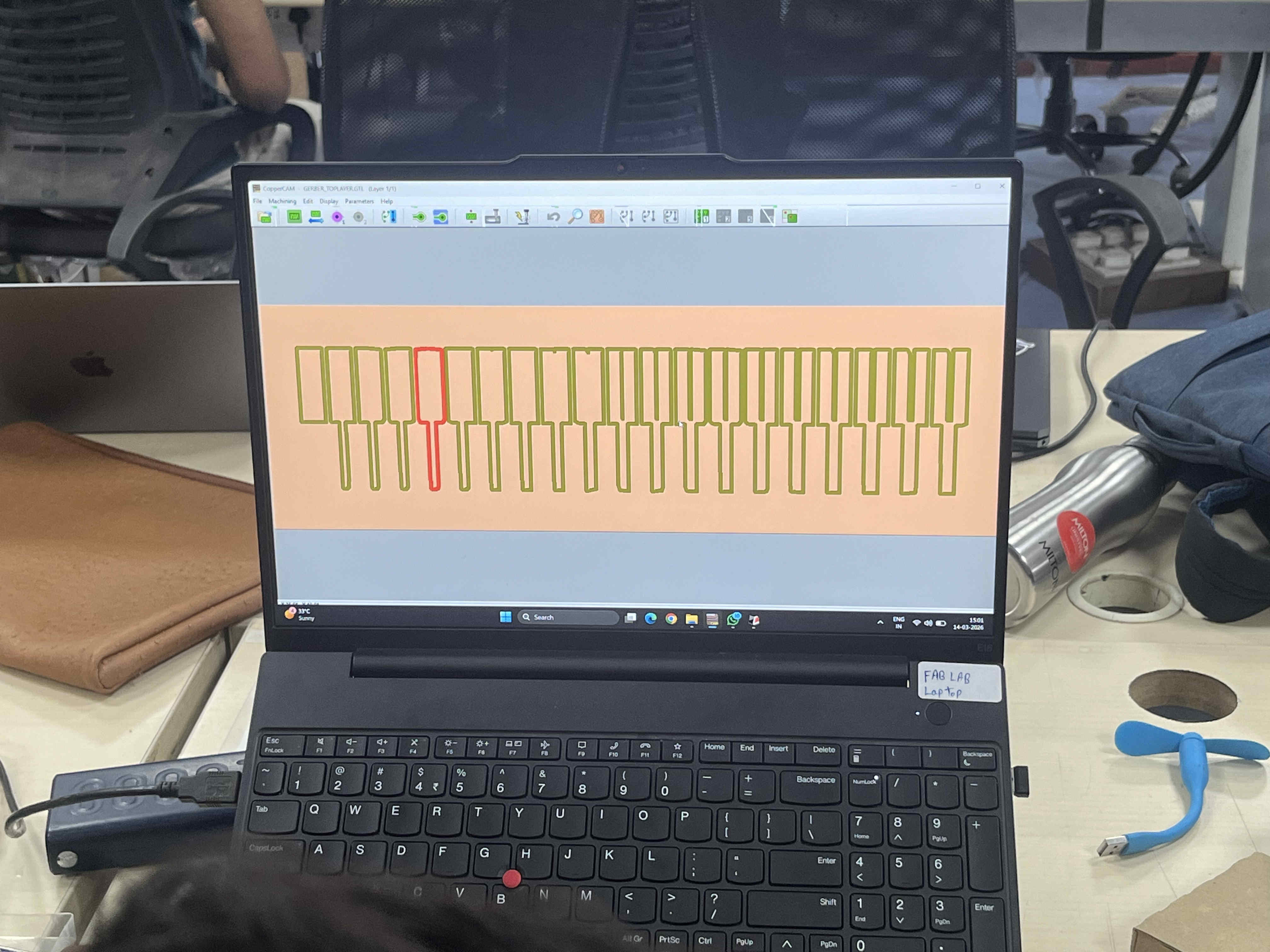
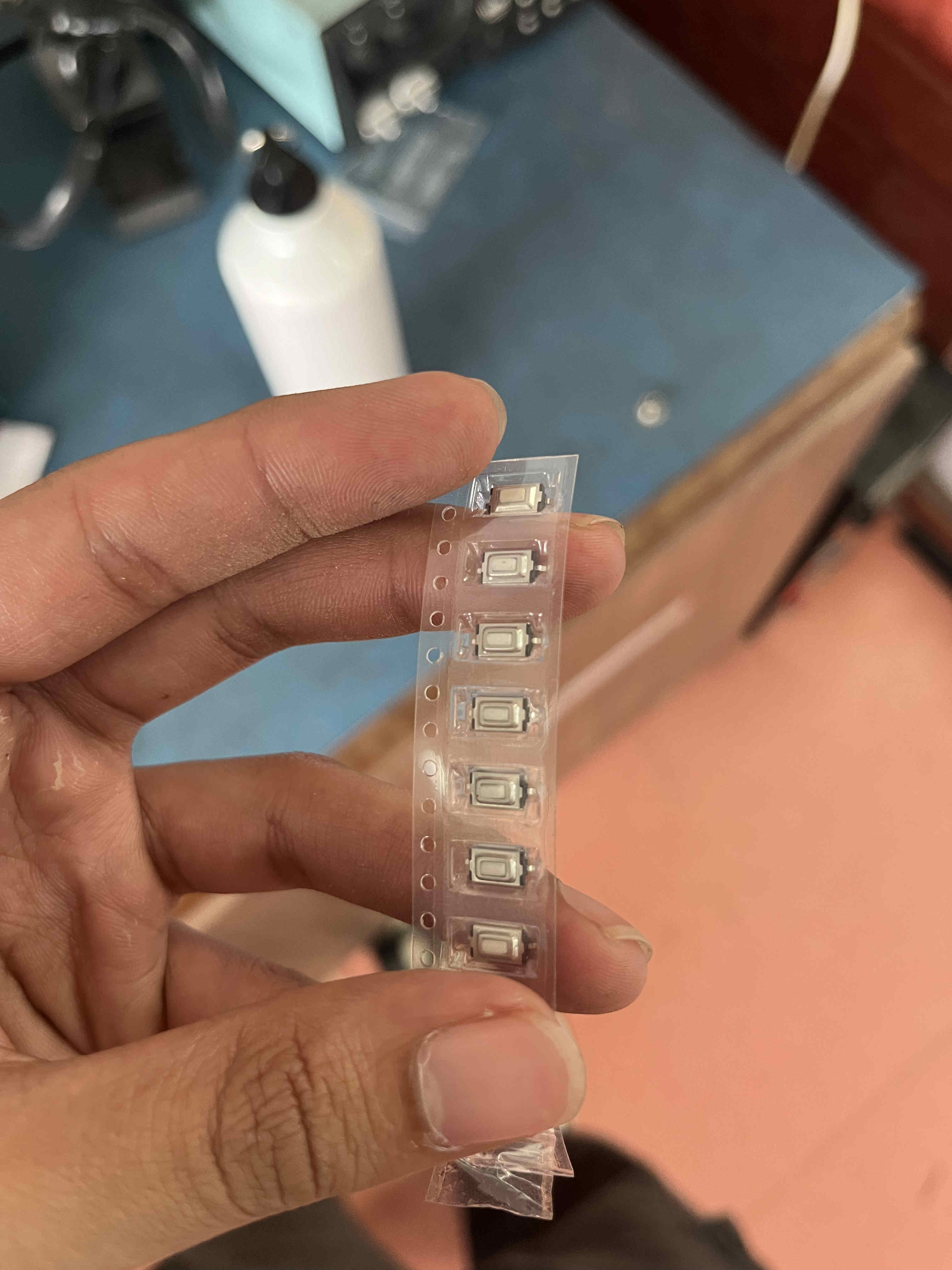
i got the track clearance as minimum .8 mm and track width as 1mm minimum .8 mmThis is a smd push button.
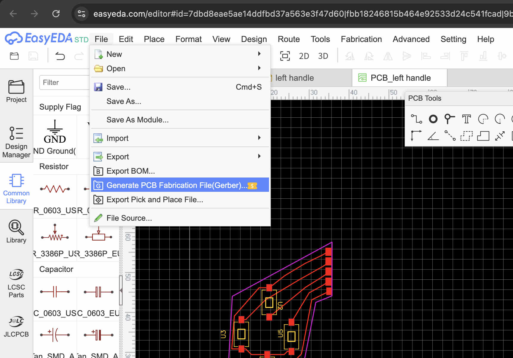
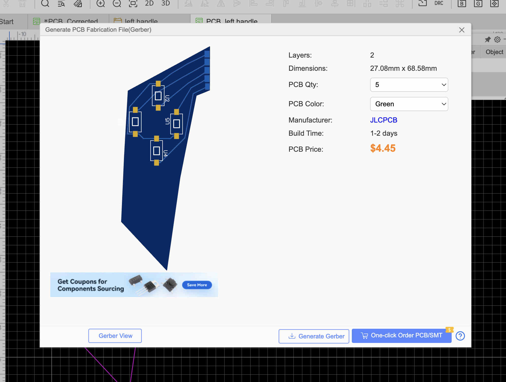
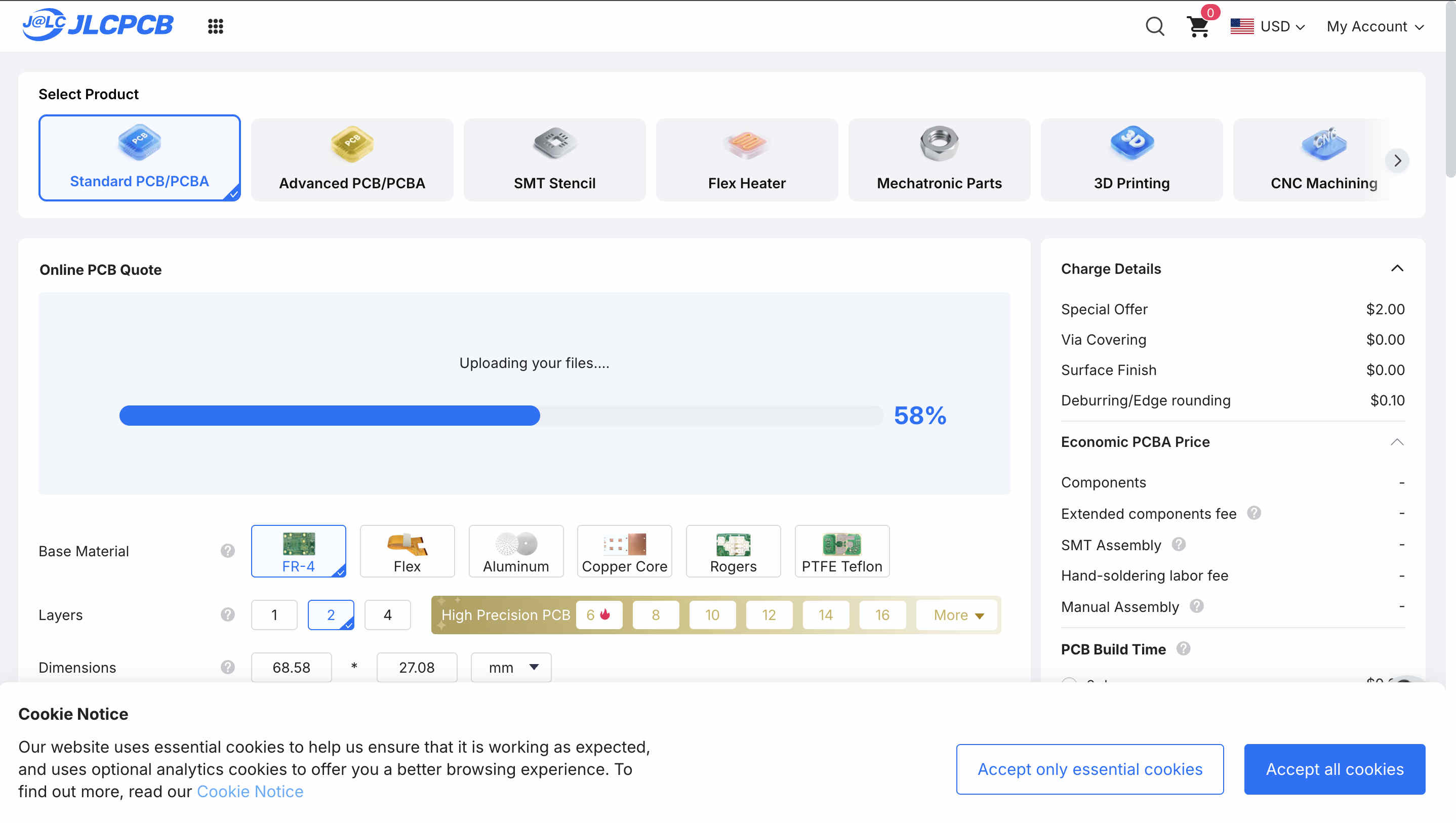
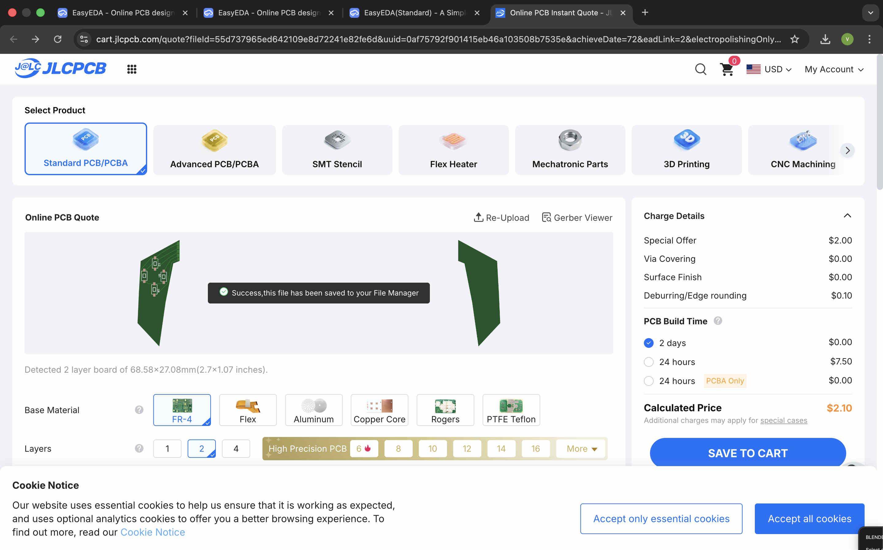
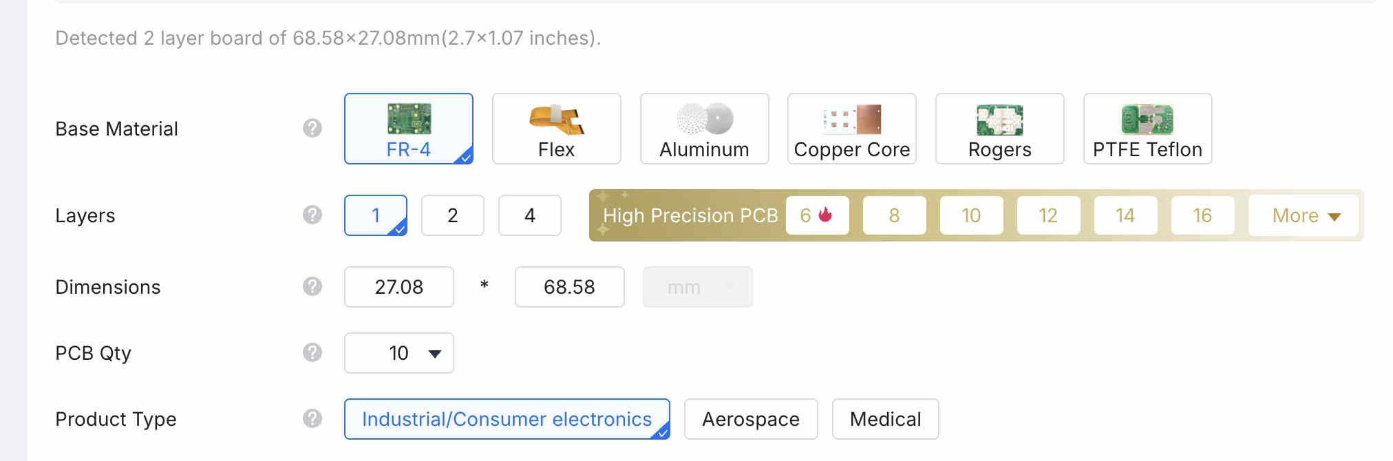
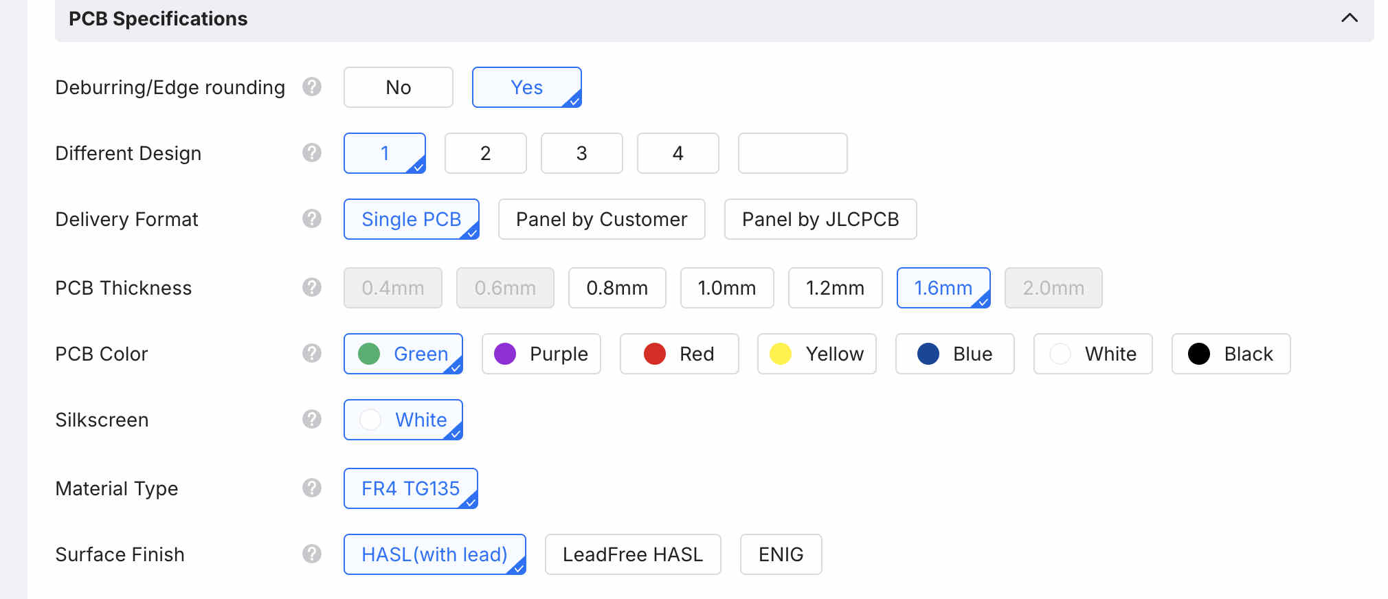
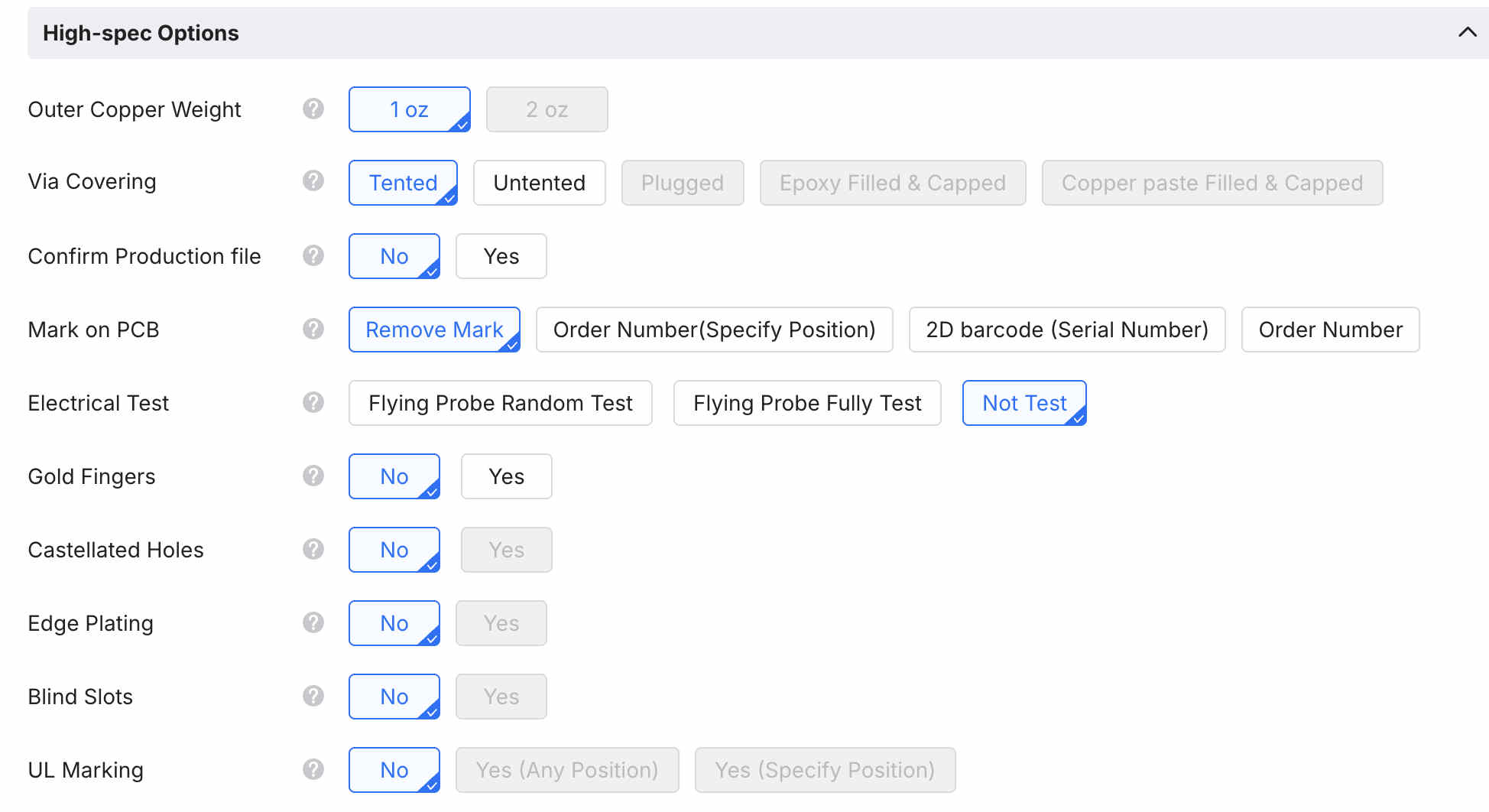
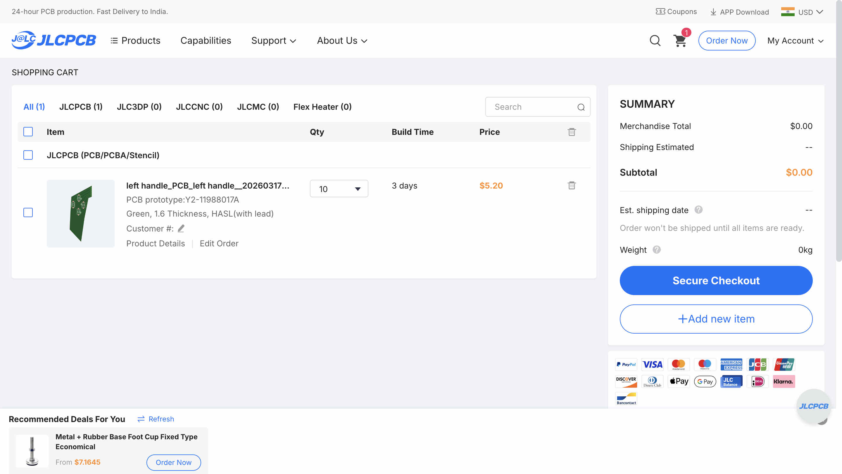
Ordering a PCB from JLCPCB
Generate a gerberclick on one click orderSelect material and typecustomise quoteDifferent options on material and type.
All these are optoions that you can customise
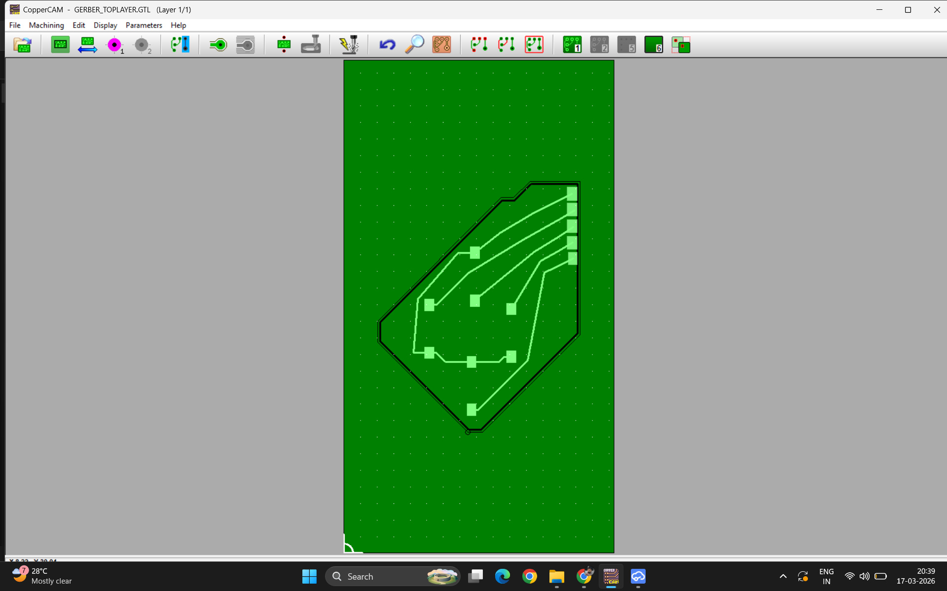
.Moving on to copper cam.
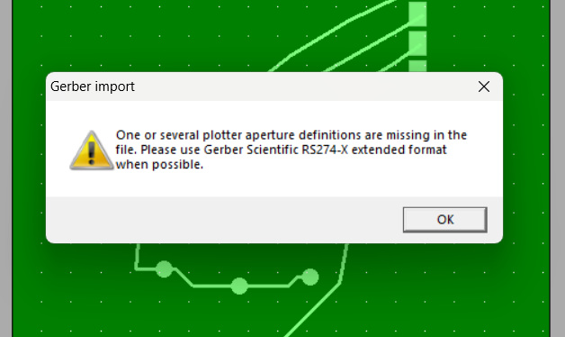
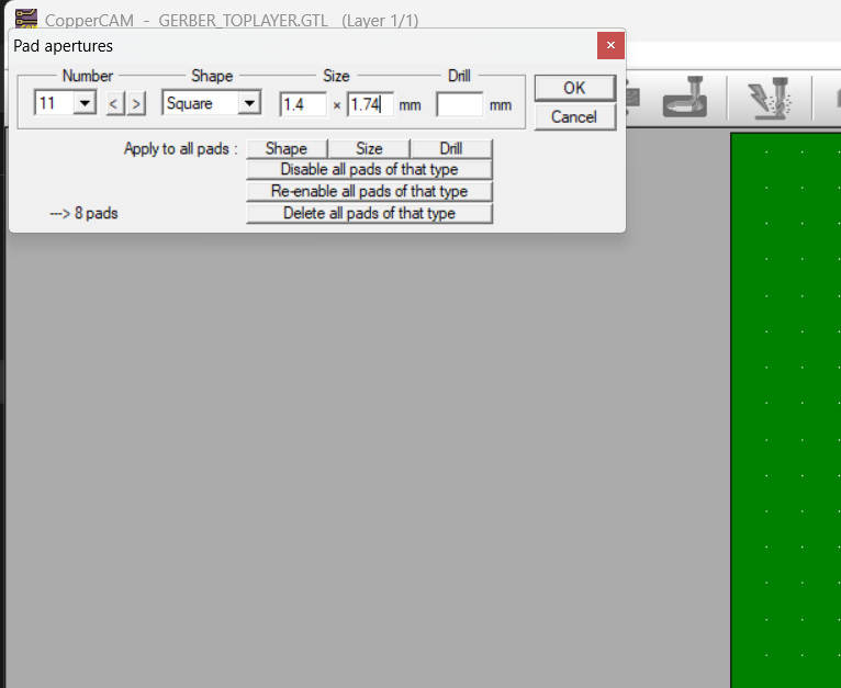
This was the final resulterror when wrong importsYou can cutomize pads on software as well.
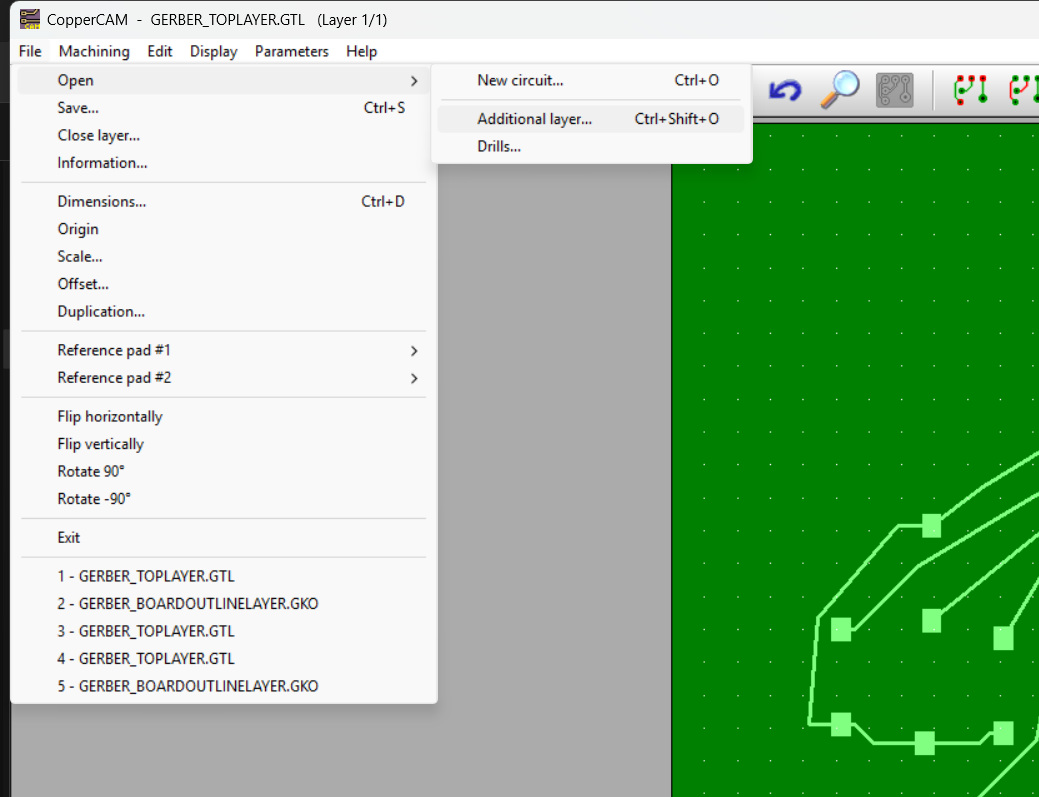
This is the correct way to open
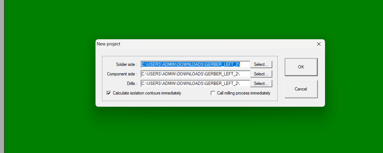
File, additional circuitAdd the correct files in the options as follows
solder side(First option) - Top layer.GTL
Component side(second option) - board outline.gko
Drills(third option) - Drill_pth_through.DRL
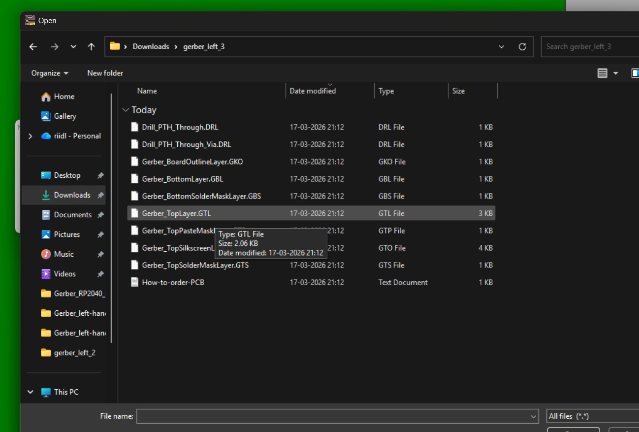
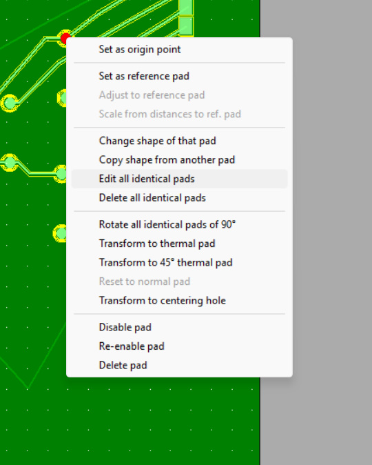
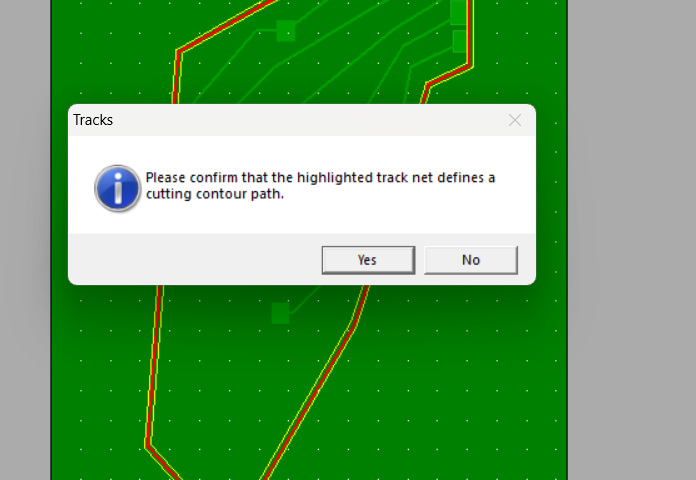
This is what the unzipped gerber file looks like.Sometime steh cutting contour does not come into the cutting layer,
right click on th eline asnd set as cutting contour.
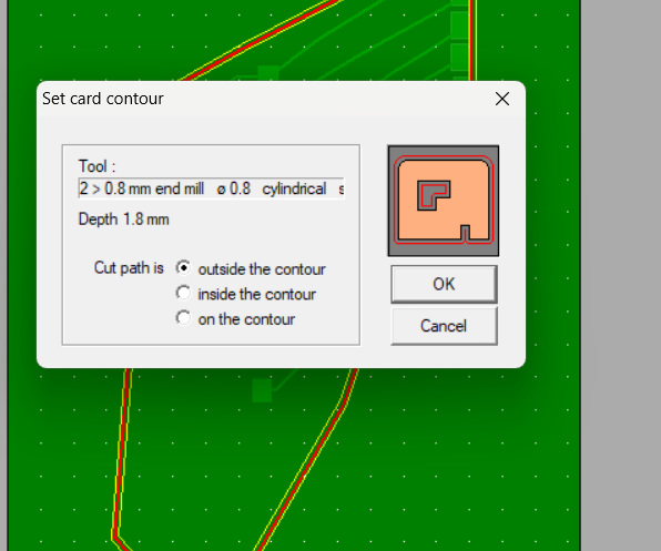
click confirmDepending on you design select crd contour settings.final set file.
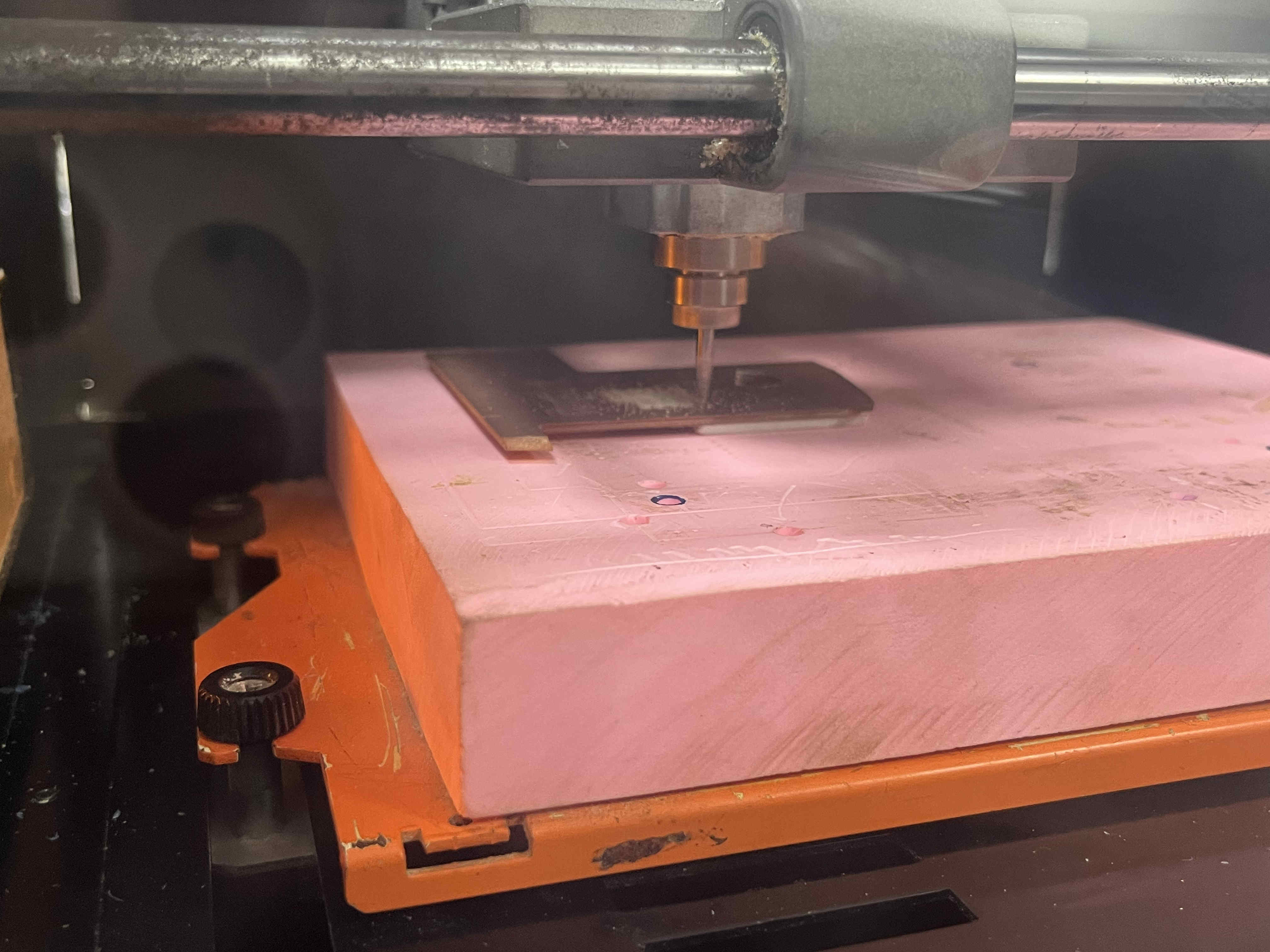
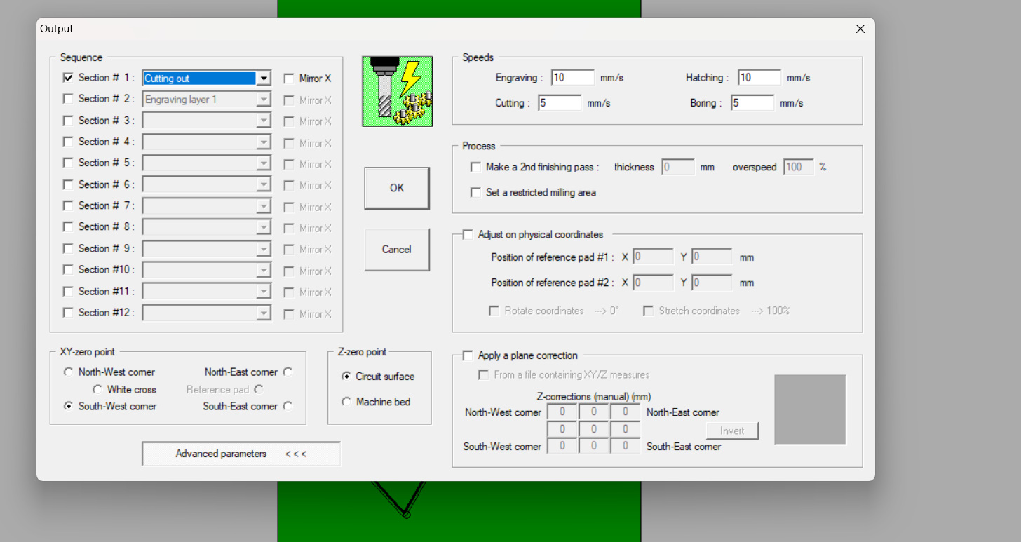
Moving to SRM-20
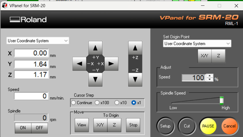
This is the v-panel to control the machine, and home Z- axis
You can home Z-axis using the paper test.
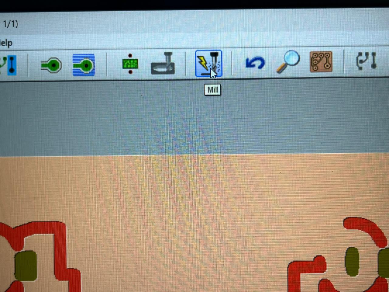
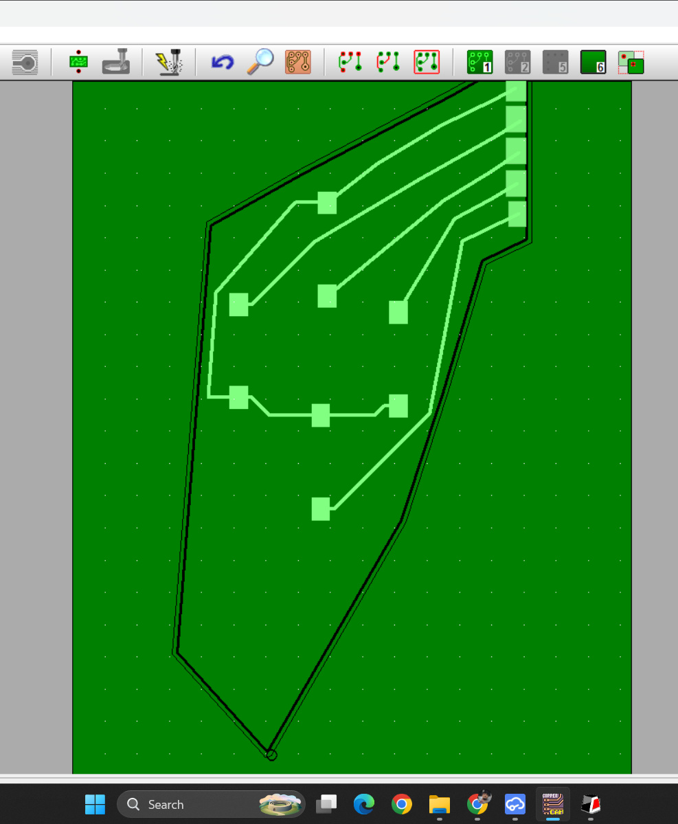
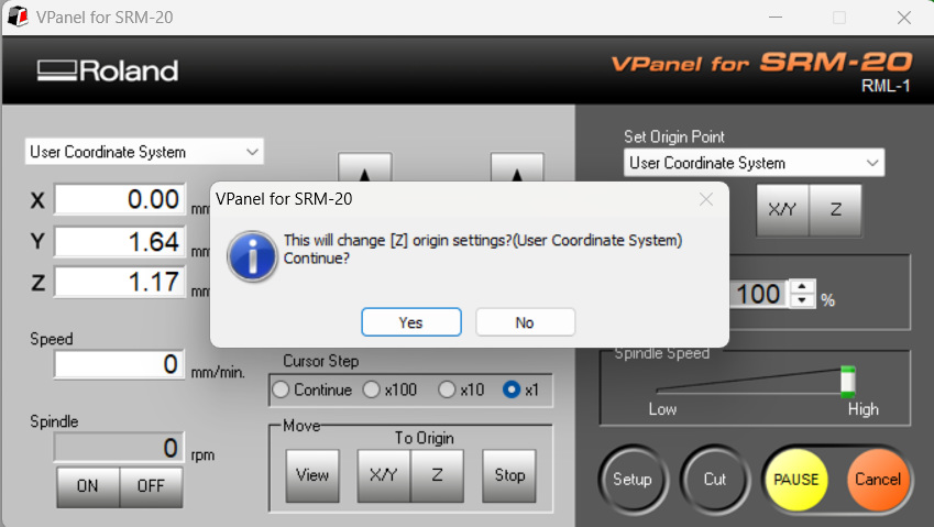
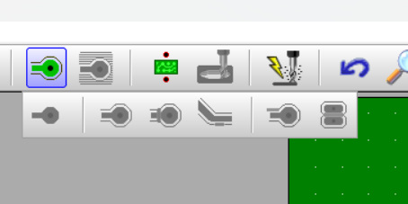
Make sure to be careful while controlling tyhe bit and spindle, excess foce on the spindle caused by innacurate movements of the bit are bad for rhe machine.click yes.In milling choose option of engraving cutting.this option is for setting up contours.set contour settingsFinal PCB.
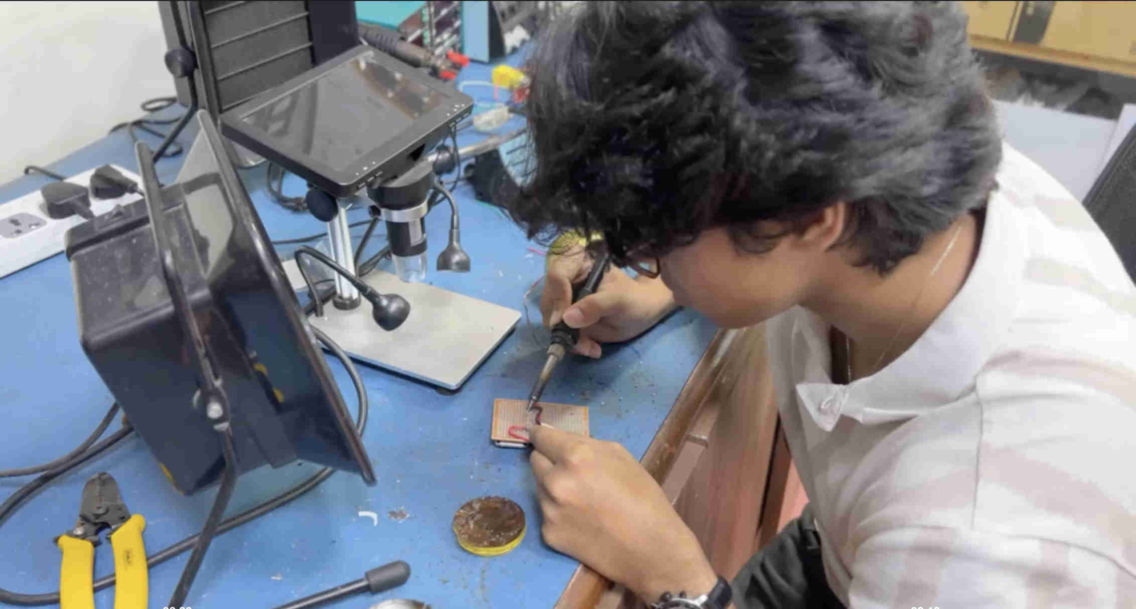
soldering and more for final proj
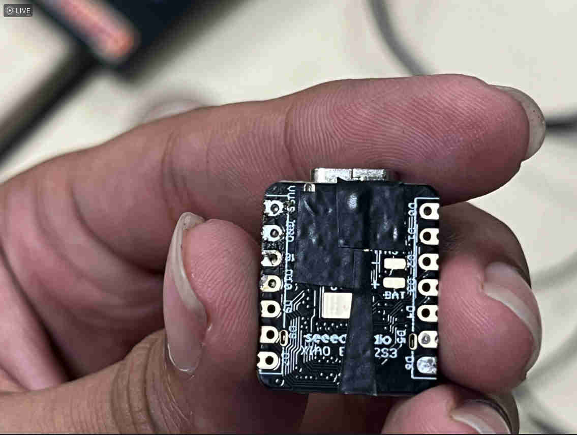
here i assemble a different board, the one i use for my final project.
This was how I prepped my esp32 s3, i highly recommend doing this as the bottom pns can catch conducting signals or misalign and short the board.
Practicing soldering on perf board with wires to replicate.
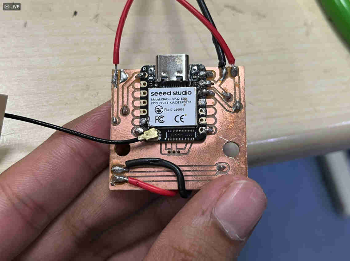
Final board.
whenever a chip like the xiao or smd components with multiple contacts is being assembled -
Alignment is crucial--
1. thus first align the board tape in place with some masking tape
2. solder 4 corners of the board with the slightest hand.
3, once done the board will be mechanically locked in place, you can proceed to solder the other connections needed.
.jpg)


