This week was about designing our own bircuit boards using various EDA tools.
Now that we understand the world of Embedding prgrams
We are onto designing our own PCB, that we can use for various inputs and outputs.
Understanding existing microcontrollers and how thier boards are designed.
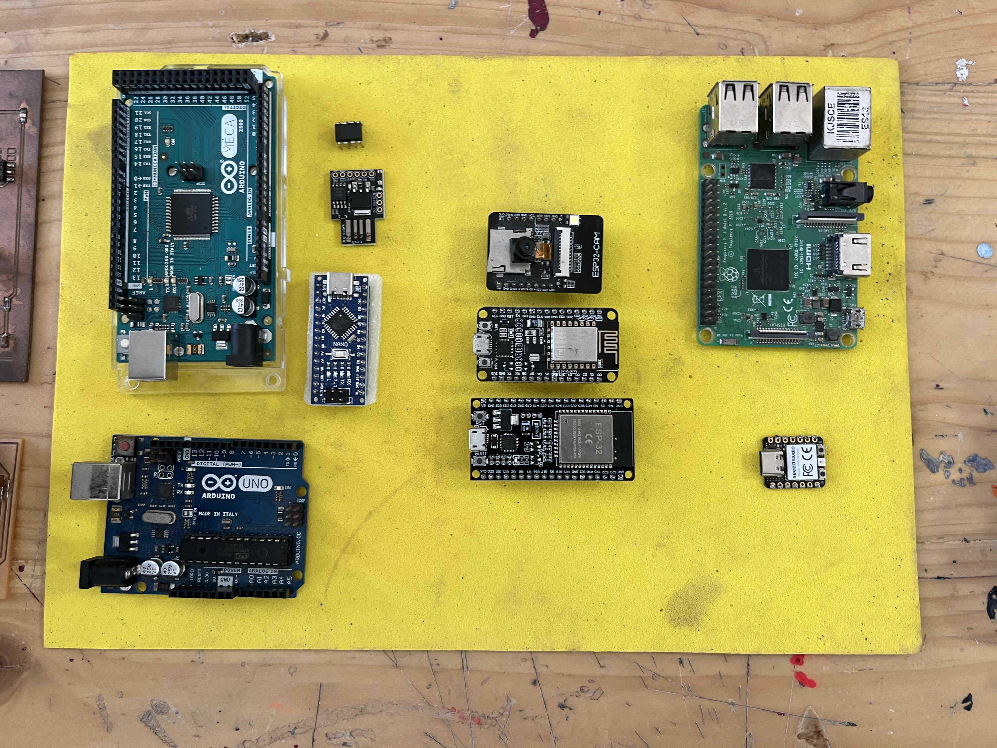
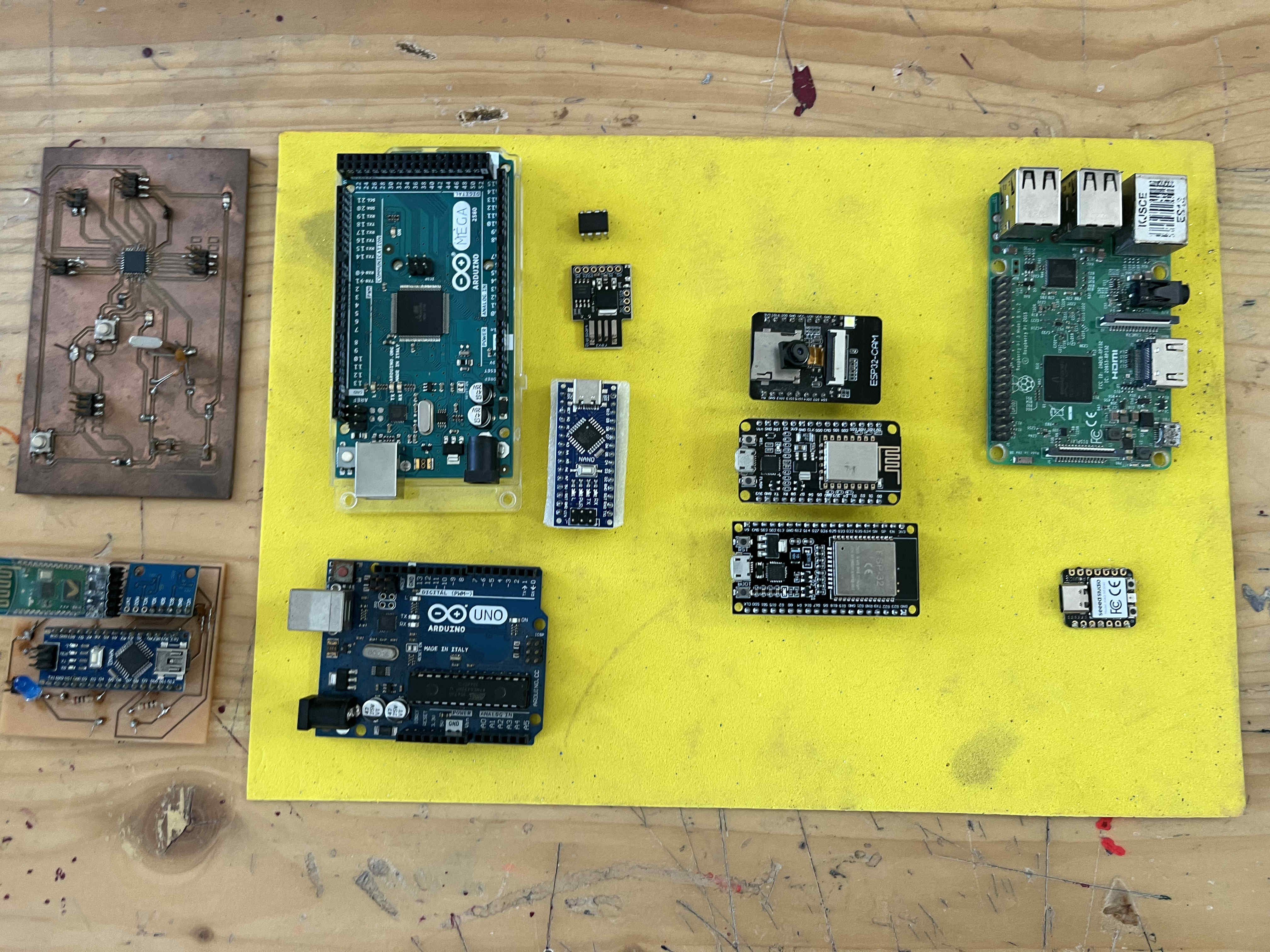
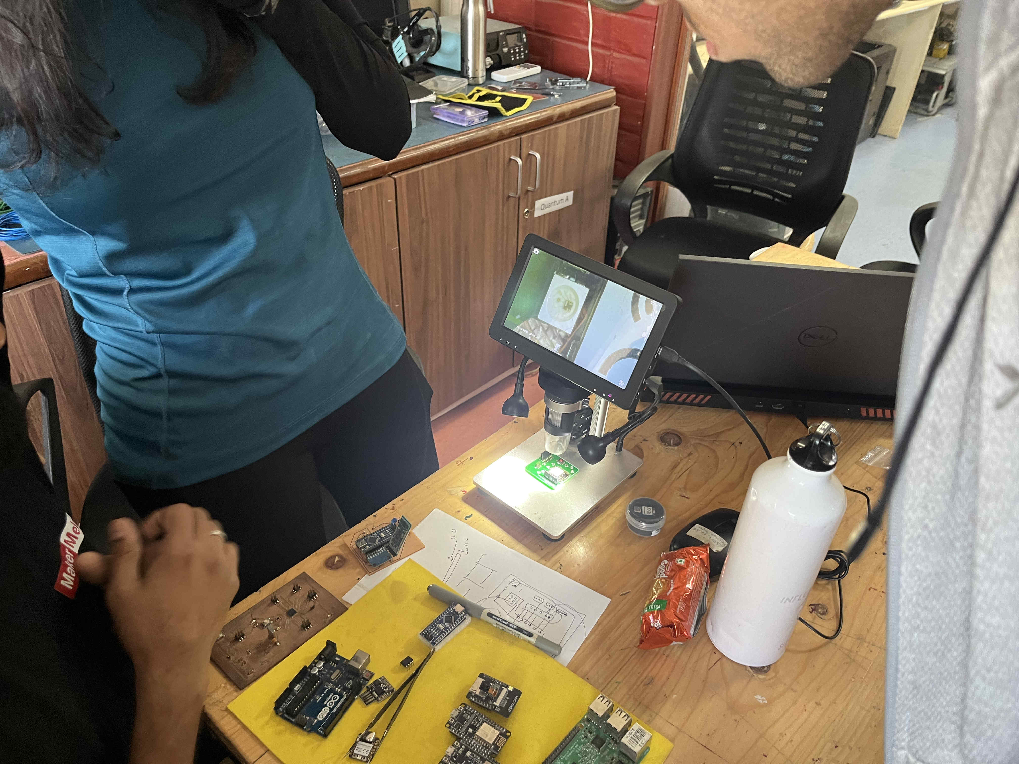
We took a look at the various controllers we had in house first.On the left you can also see Some in house designed and milled Arduino,s made using the same chips and only the nessecary outputs and inputs.Using out microscope to view finer and deeper details into LED'S, resistors and more
Understanding easy EDA and workflows to create Circuit boards
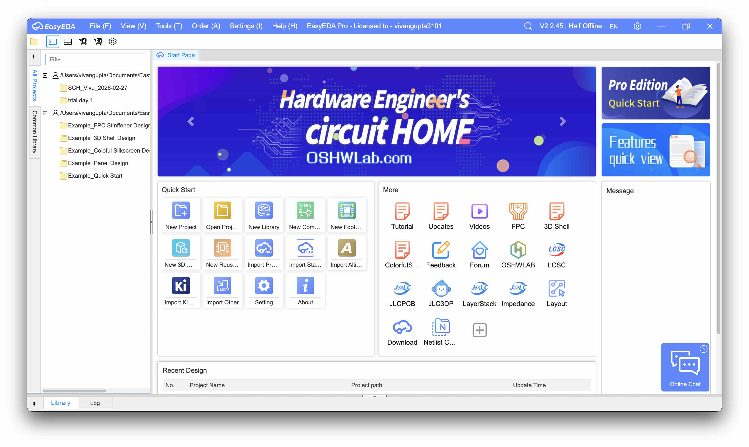
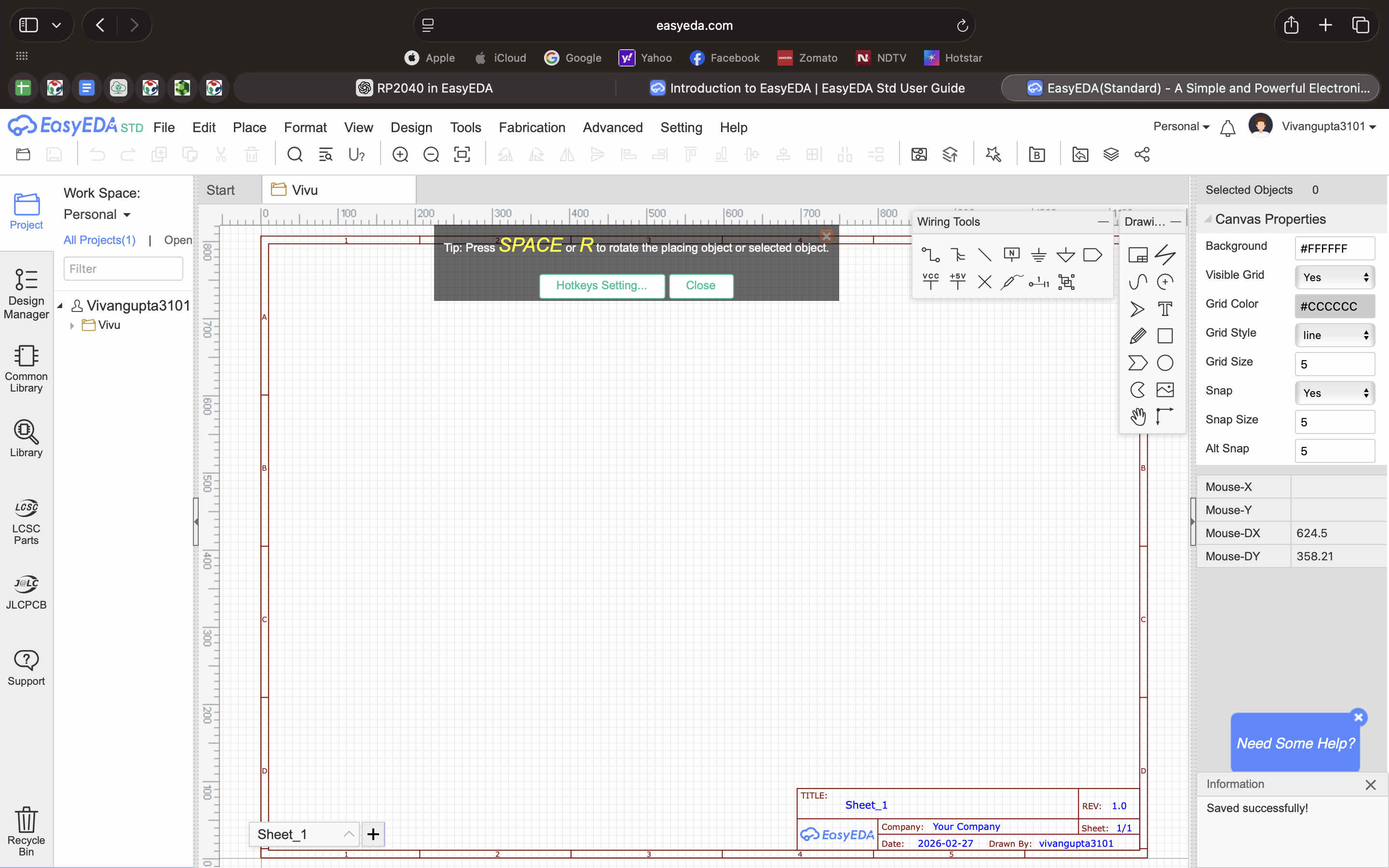
Installing Easy eda
https://easyeda.com/page/downloadInstall Easy EDA using this link, pro or std version both are fine
While pro is great
It has some restrictions.
For example -
STD version has user uploaded schematics, thus most equipment that you are looking for will be readily available
Pro on the other hand has removed this feature, as many faulty schematics crowd the platform as well
Don't worry, I have mentioned in the following documentation a work around for ARM chip mac users that only have access only to pro models
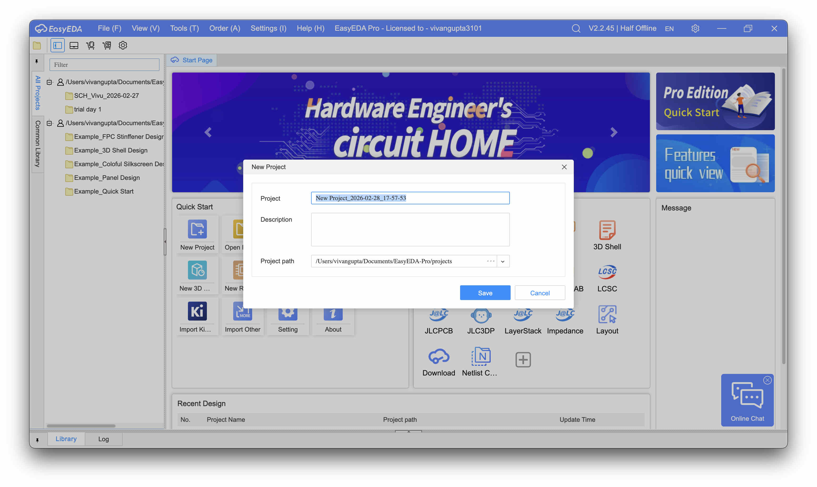
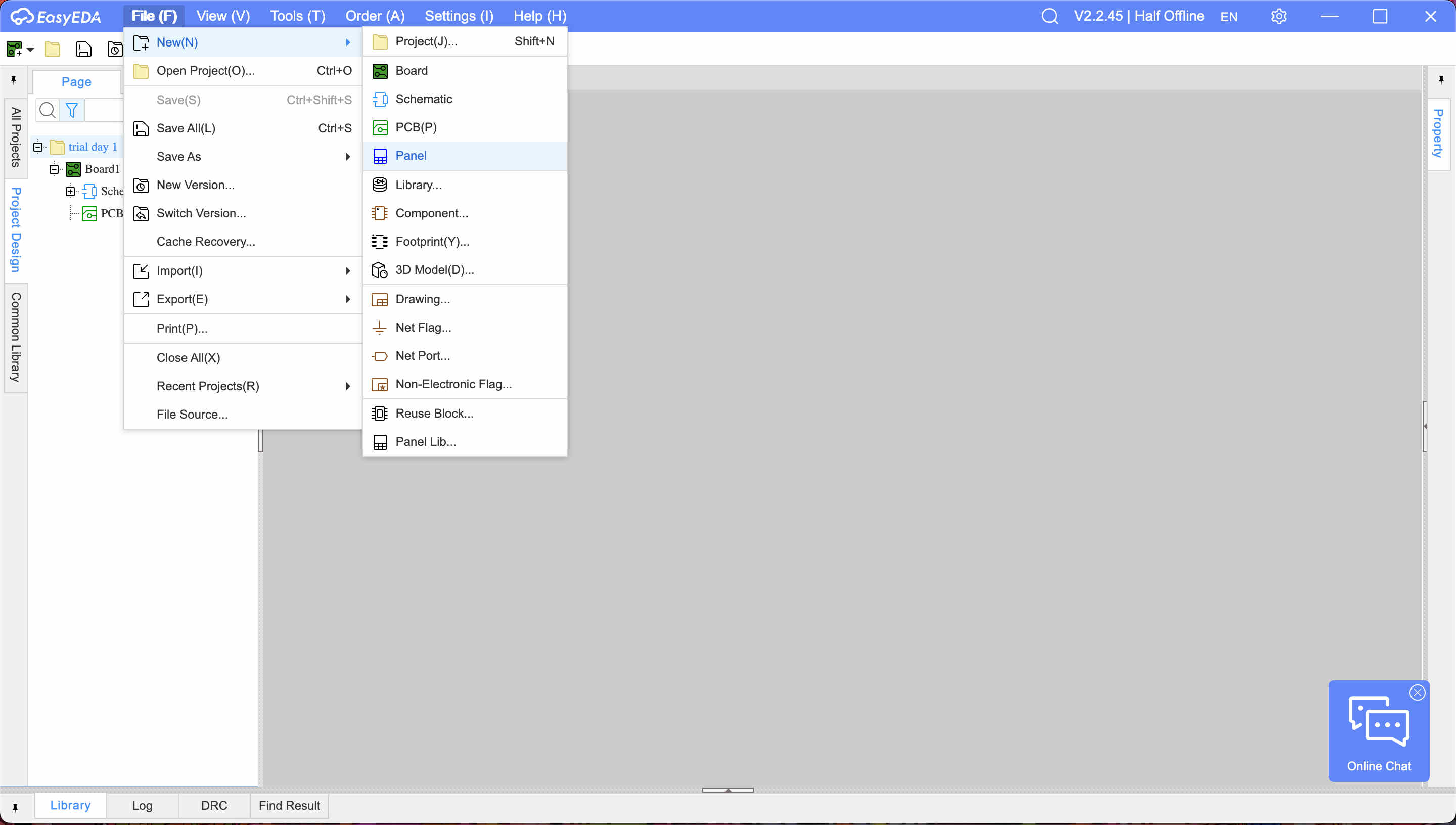
However this method is very tedious especially for pcb's that requires a tonne of components, thus arm chip users..... STICK TO EASYEDA ON THE BROWSEROnce you open the application you will be presented with this pageClick on new project and name your filesOnce your project opens you can start by going to file- new- and then whatever you require
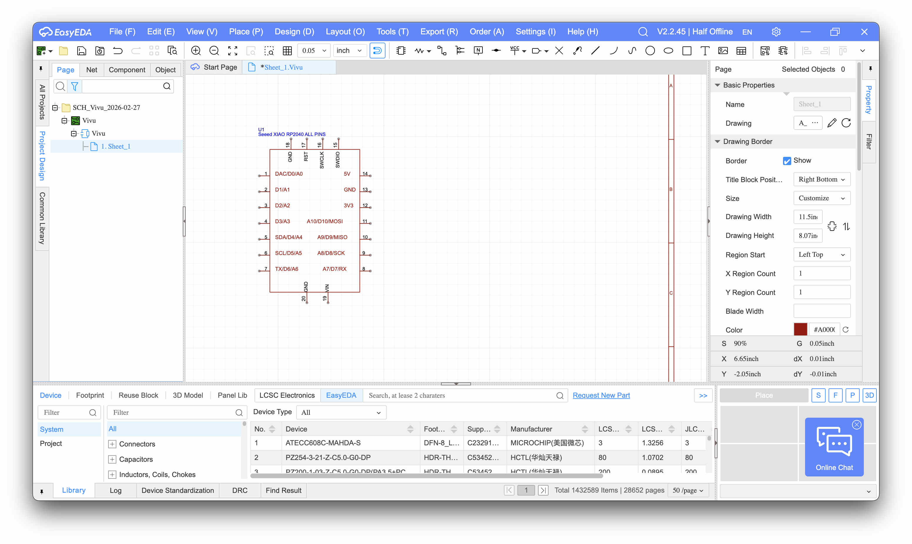
Schematic and common library is automatically loaded on te left side of teh software
You can open schematic first to design a circuit board
Library is open at the bottom as seen below
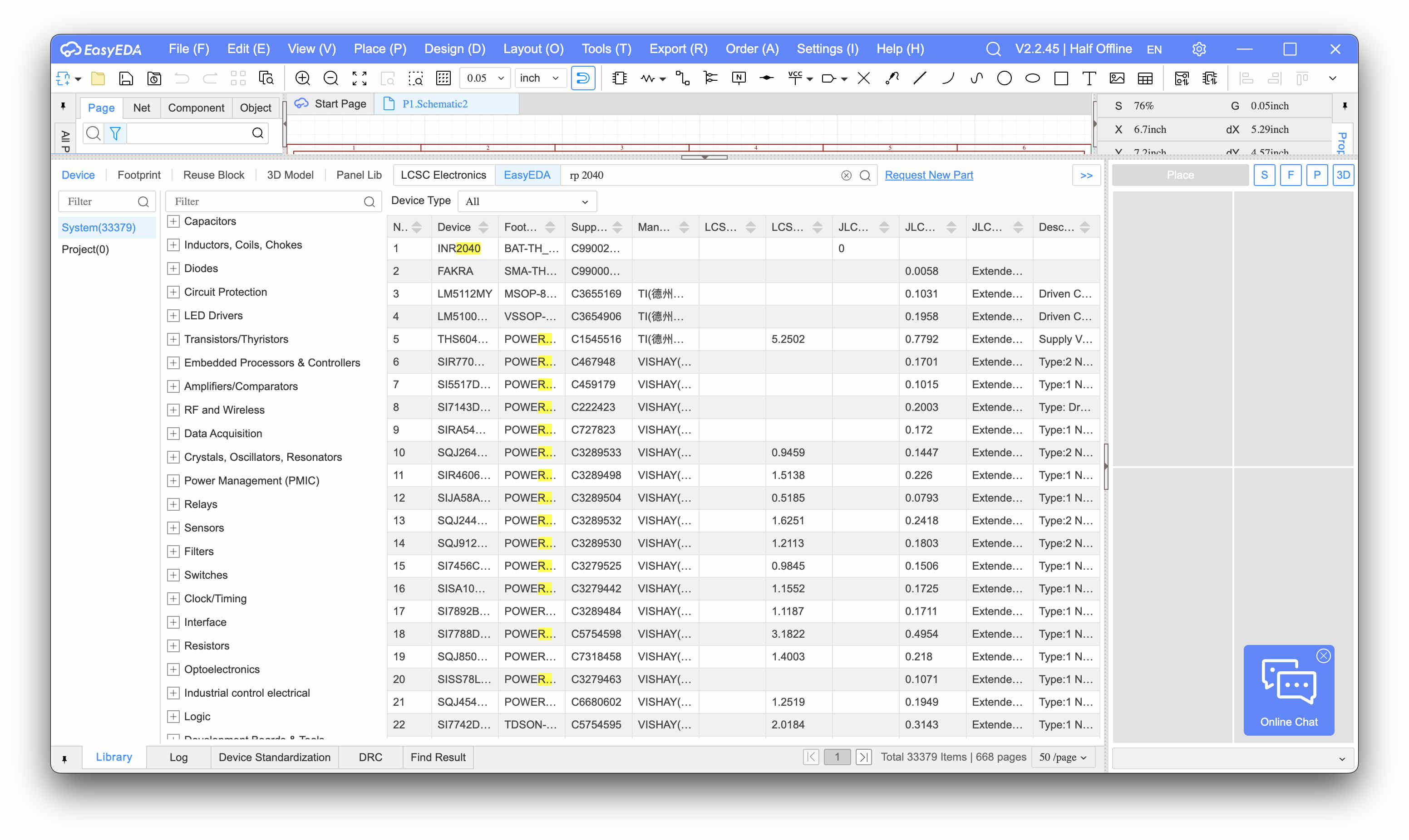
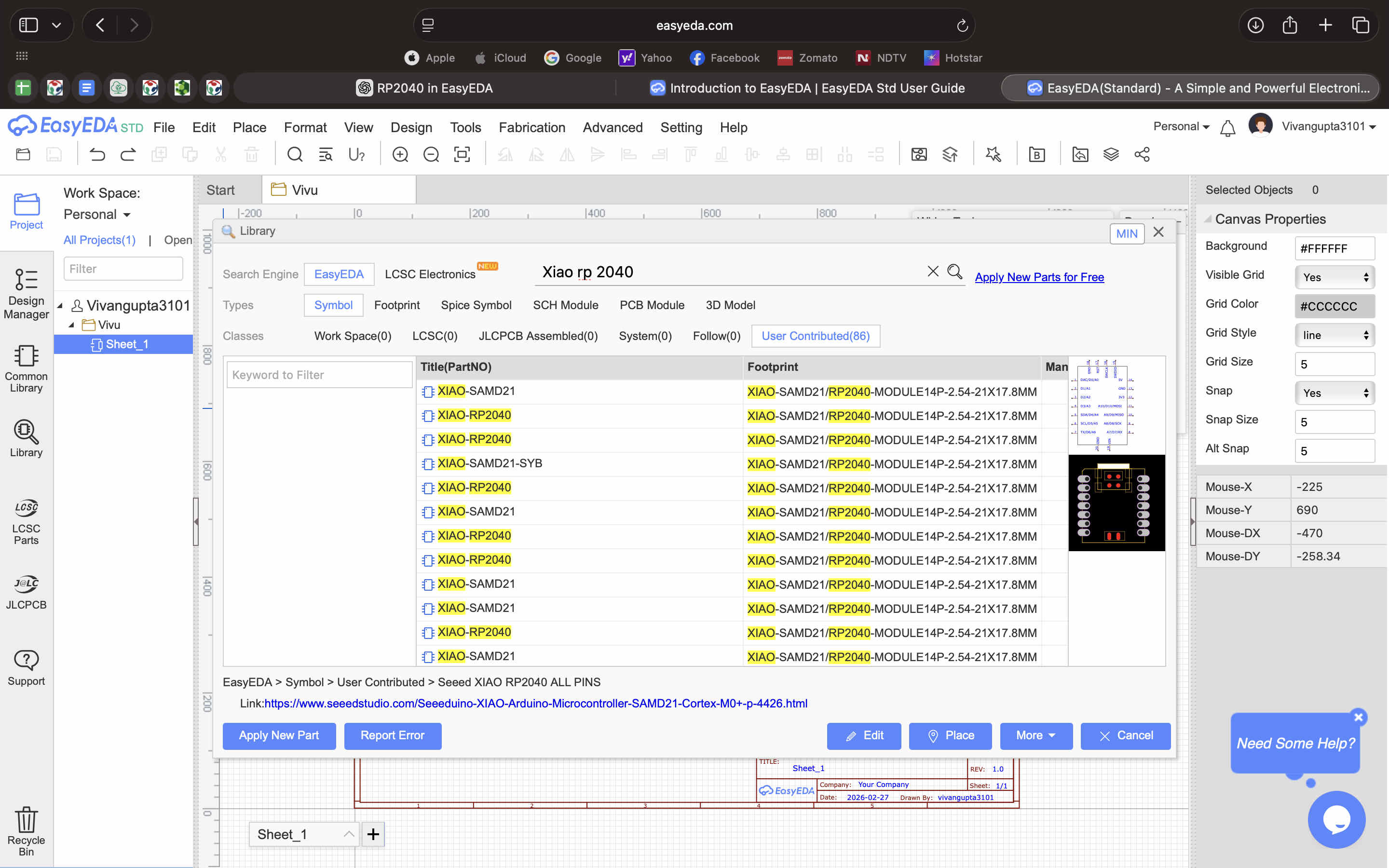
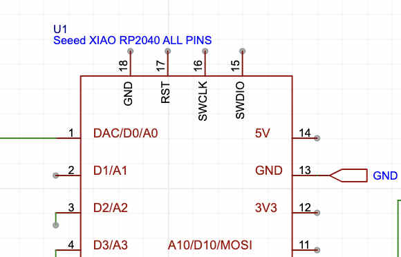
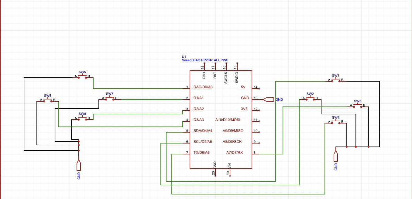
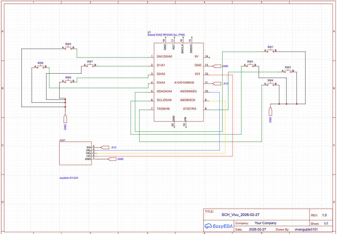
For trials we try to place a rp 2040 oard by xiao to design a perpheral board for it
Error- I could not find a suitabel schematic for my Seed xiao rp2040
This is because of what i mentioned before-
Pro versiom only has JLCC assembleable parts and no user uploaded schematics
Workaround
On my browser I opened the standard easy EDA version
Make sure to login with the same account as your pro version
Here - You will find an extended larger library that you'll find most schematics pretty easily
As you can see the top panel has a user contributed section, & other filters that are not available in the pro version
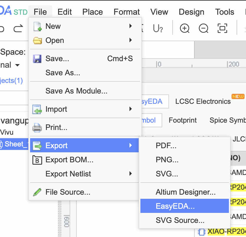
Once you have Parts that you want in your file, export this eda file Open your Pro version installed on your system.
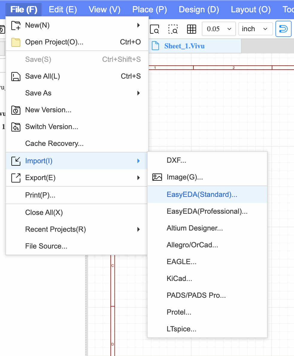
Go to import - and improt easy eda(standard)
Select the json file which was exported VOILA!!!!
This method ended up being more tedious later on so take it with a pinch of salt
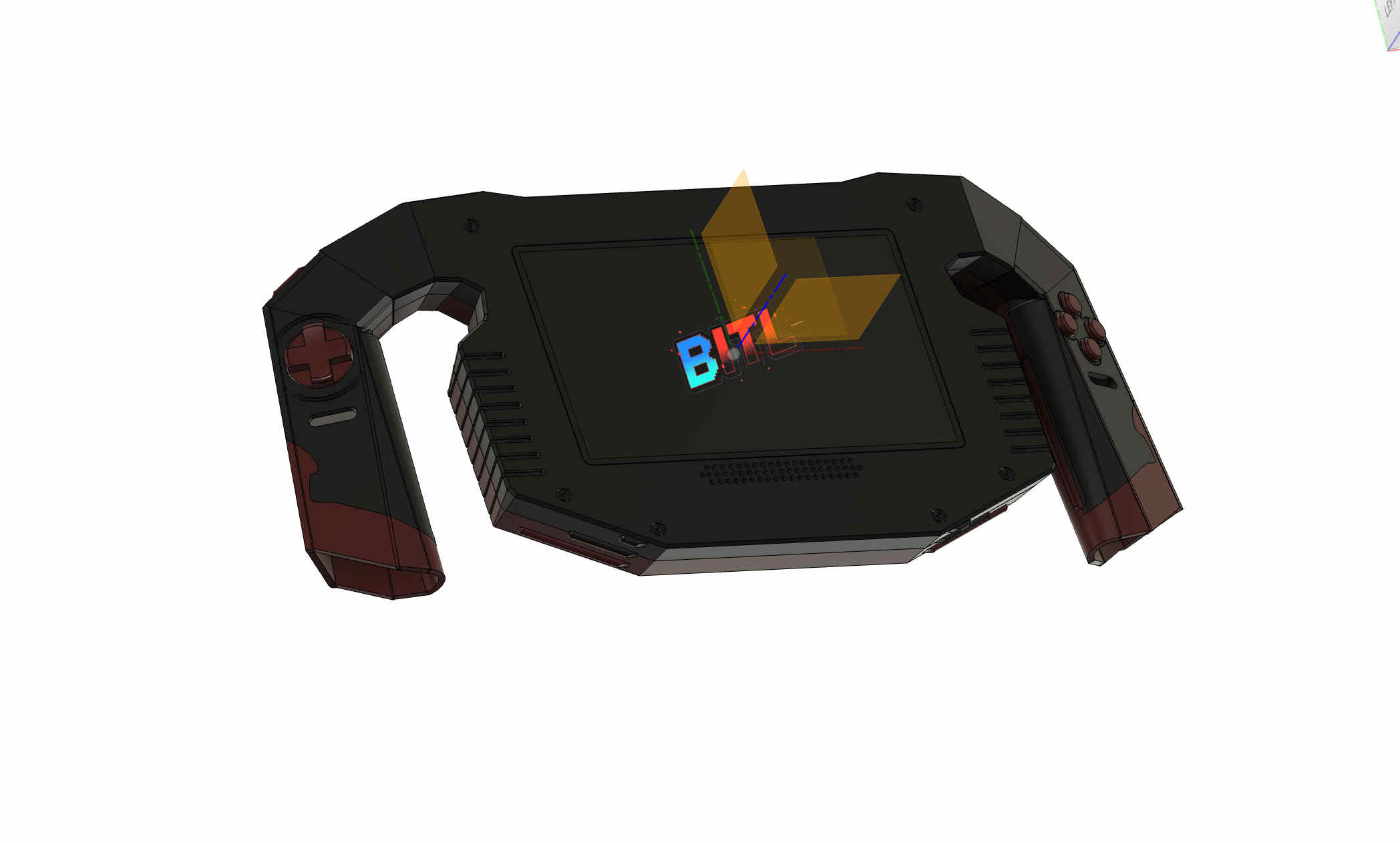
Designing for a gaming console.
I decided to design a pcb for an older project that I had designed
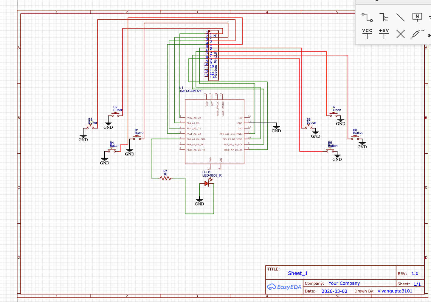
Which was a 90's style handheld gaming console
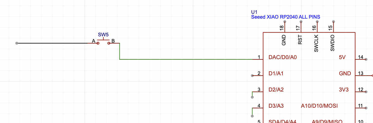
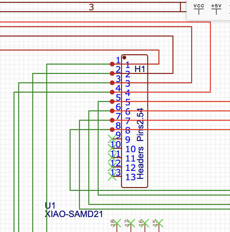
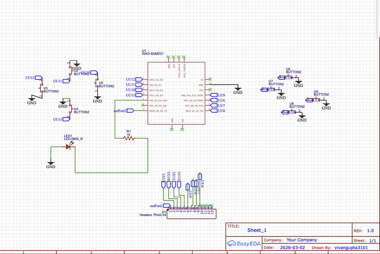
We start by adding buttons and eiring them to Digital pins individuallyTo keep you schematic non chaotic and clean, you can use net ports, you can cdonnect one end of the net port to the desired pins
And the other on the desired connection
Remember to keep the naming for each net port same
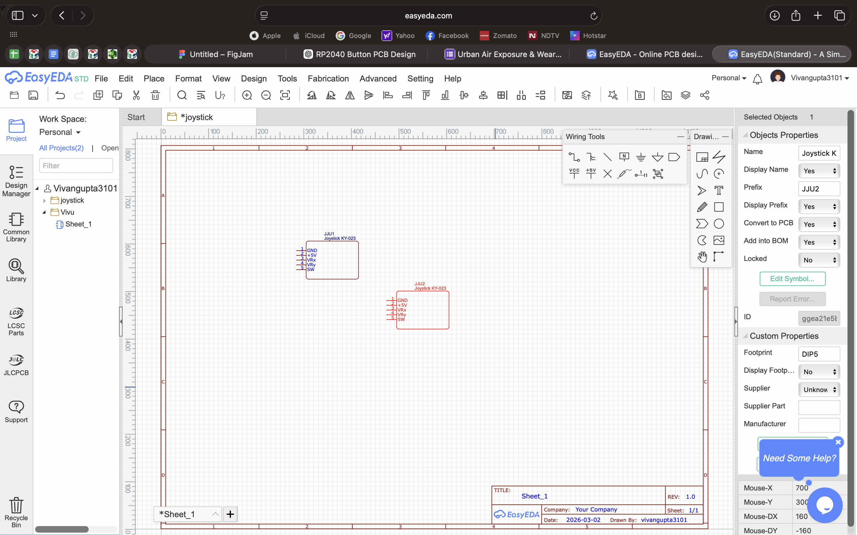
You can see how we do it hereBasic schematic is ready.I tried adding a joystick by the same mehtod from EDA onlineWiring it on EDA proSince my design had a bend I got on a call with my instructor to explore bending pcb and It's process
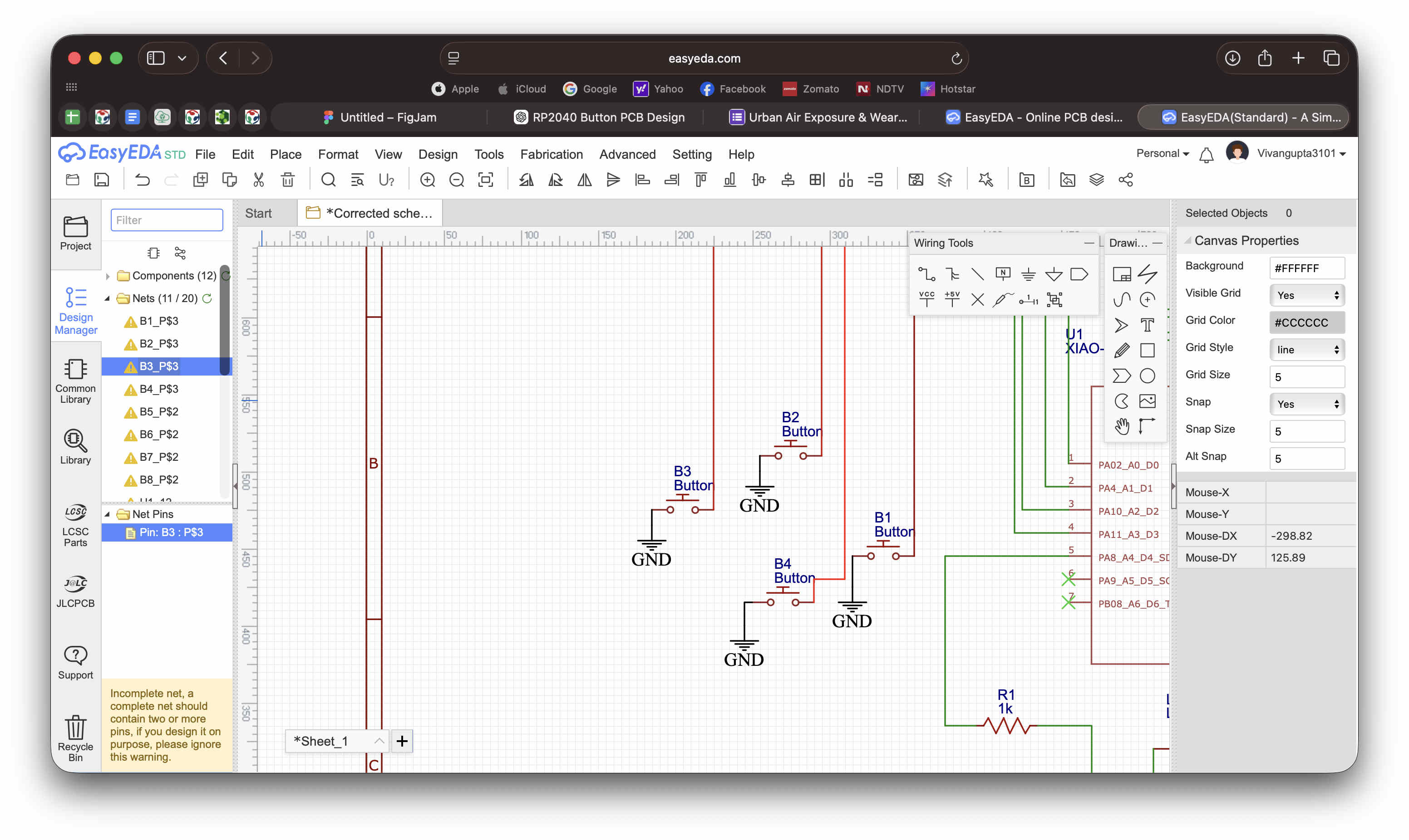
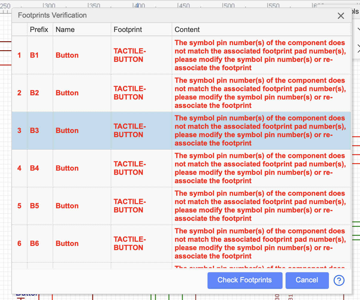
Right about here when i tried to run the DRC. i realised importing schematic did not import the footprint as well, that would be another step to import
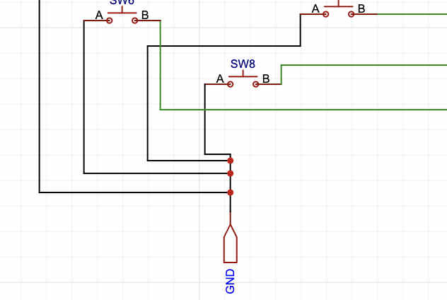
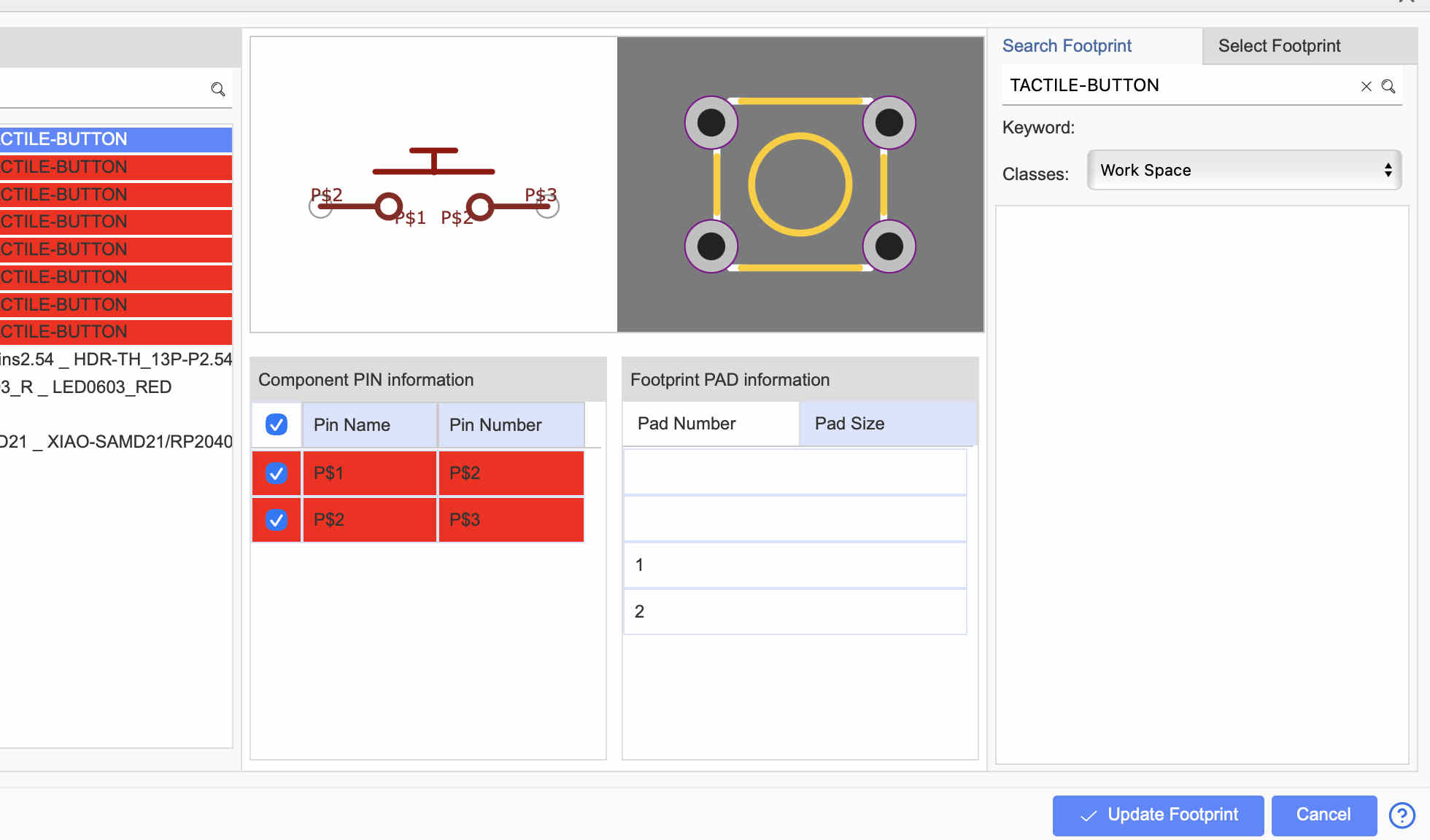
With the hassle involved with pro I decided to shift to EDA std onlineRewiringAgain on DRC, i got some errorsI quickly realised that i had not closed the un-used net portsIn easy EDA, if you have points of a pcb or header or any part that is unused, make sure to cross these endings to avoid errors.I ran into another issue with my buttonsMy footprint for the button and the schematic naming was completly haywire and basically it was not the correct part
Remember to check footprints if you take parts from user contributed stuff. Any issue later requires going back to the drawing board again
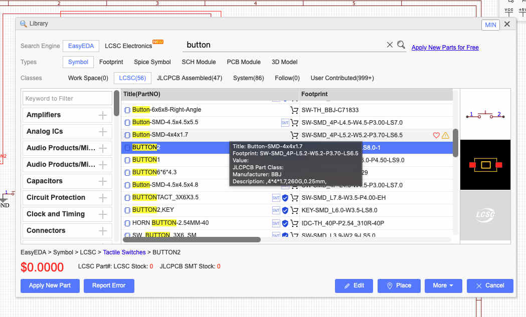
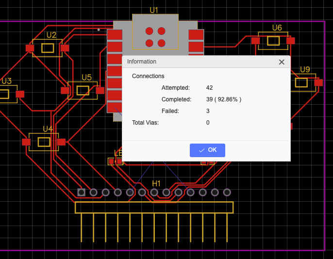
This time I chose a button from the LCSC assembleable libraryAfter wiring again I ran DRC and converted the schematic to a PCB.
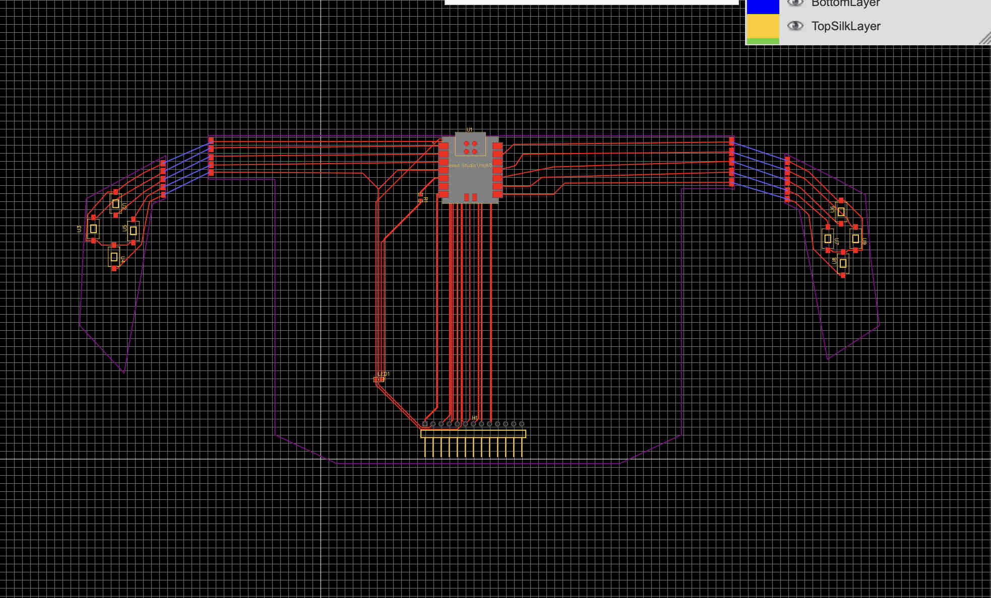
this was the result
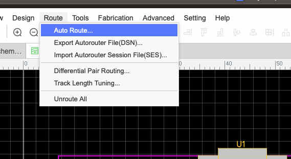
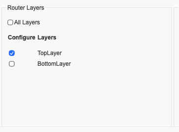
We can now autoroute our pcb Since i was doing a low fidelity not so complex pcb, i chose only top layer,
IF you plan to do a only top layer smd pcb, remmebr to untick the bottom layer button
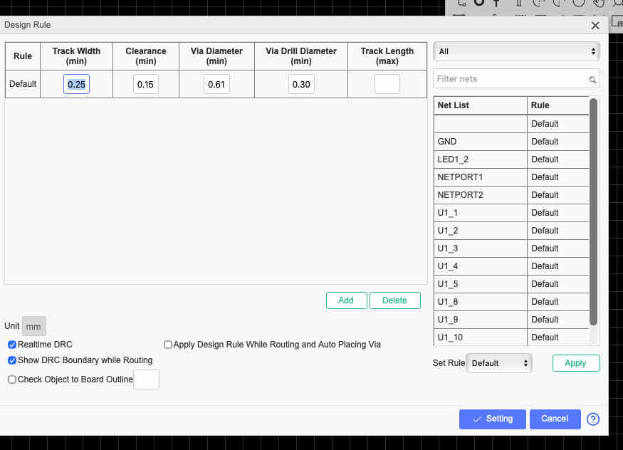
Under design rules set the parameters and factors of your machine and pcb
These settings are optimal for the SRM-20 and cutting standard fr4 copper clads(all minimums)
track width- 1 mm
clearence- .8mm
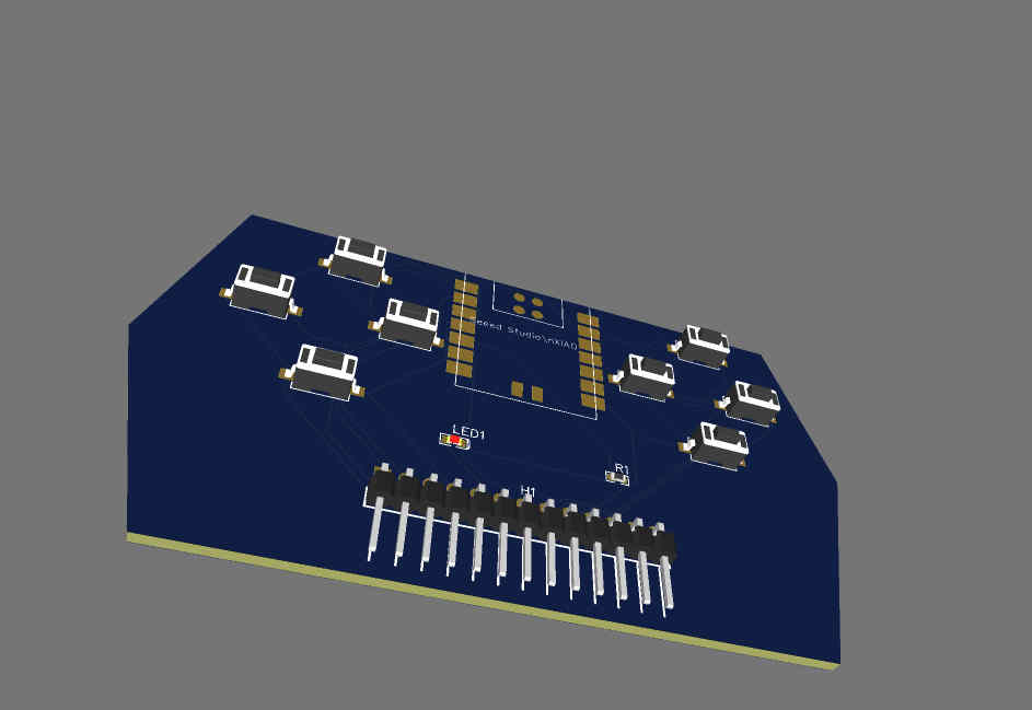
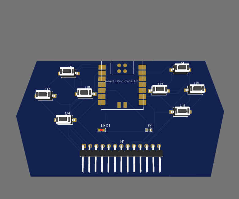
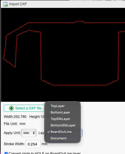
Autoroute result3D view of pcbSince we needed a custom shape, we can import a dxf outline of the desired shapeRemember to change layer to bottom outline while importingAutoroute and, 3d view of pcb.
Hero shots
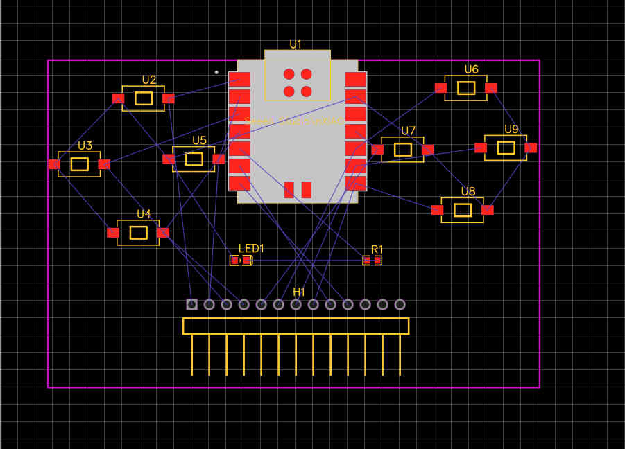
Here is the full circuit diagram of the designThe tracks here are extremly thin and when manufactured had alot of issues with conducting signals properly, as the slightest scractes made contact tracks fail.My plan was to mill out 3 pieces then wire them after mounting to integrate the bend of the pcb.
Bending pcb with solder as bridges was difficult thus the hard wiring method was best
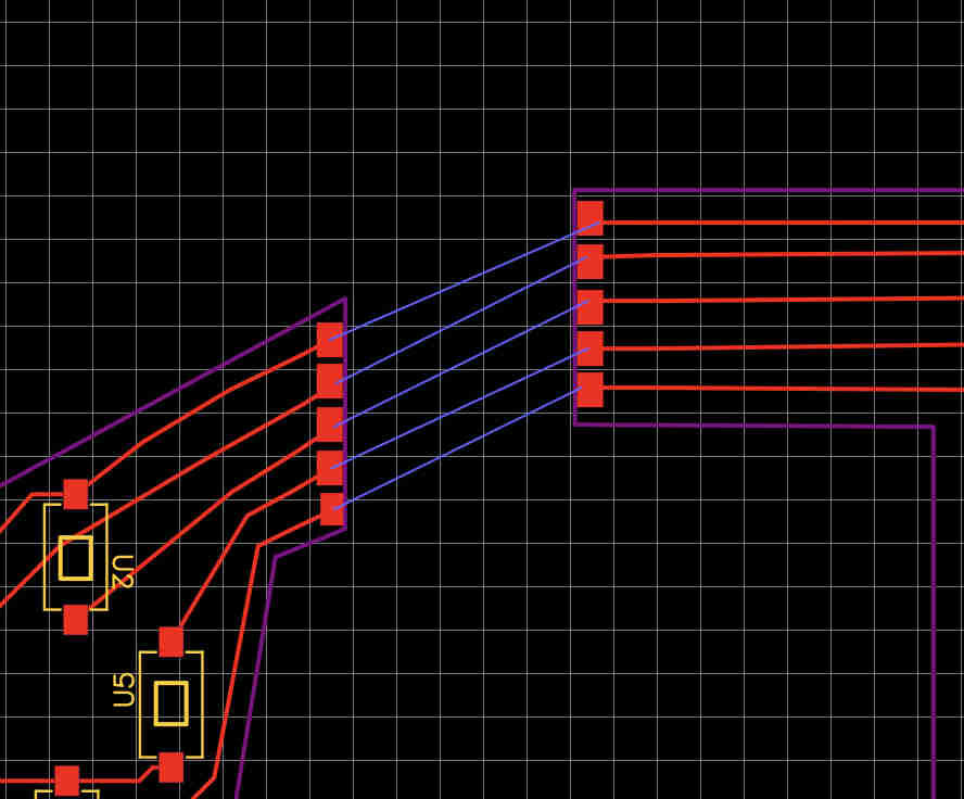
another learning was orientation of parts, to optimise space
As you can see here some butons are flipped so that their ground pins align, making it easier to take out common tracks to the xiao further optimizing the space.
Placement and orientation of parts is just as important as board outine design.
For through hole componenets like resistors and LED's you can use hacks like these, orienting it in a way such thst a track goes through the centre.
This is especially useful in single layer PCB's. where overlapping tracks become a hassle.