ELECTRONICS DESIGN
Group Assignment
- Use the test equipment in your lab to observe the operation of an embedded microcontroller.
Individual Assignment
- Simulate a circuit.
- Use an EDA tool to design an embedded microcontroller system using parts from the inventory, and check its design rules for fabrication.
- Extra Credit: Try another design workflow.
- Extra Credit: Design a case.
Group Assignment
This week focused on hands-on use of professional lab equipment to analyze, debug, and understand real microcontroller-based circuits. The goal was to measure electrical parameters, visualize signals, and interpret communication between devices using industry-standard tools.
You can access the group assignment here.
Lab Equipment Used
Digital Multimeter
Used to measure voltage, current, resistance, frequency, and continuity. It was essential for verifying PCB traces, checking 5V and 3.3V power rails, testing components, and detecting short circuits before powering boards.
Digital Oscilloscope
Used to visualize real-time waveforms and analyze signal behavior. We measured frequency, amplitude, duty cycle, and waveform shape. It helped us understand PWM signals, timing behavior, and signal stability.
Logic Analyzer
Used to capture and decode digital communication protocols such as UART and I²C. It allowed us to observe real data transmission, analyze timing relationships, and decode serial communication automatically.
Function Generator
Used to generate controlled sine, square, and triangle waveforms across different frequencies and amplitudes. It was tested using a piezoelectric crystal to observe vibration and sound generation at various frequencies.
Programmable Bench Power Supply
Provided regulated DC power with adjustable voltage and current limiting. It was used to safely power microcontroller boards, measure current consumption, and protect circuits from overcurrent damage.
Practical Experiments
We used a Seeed Studio XIAO RP2040 to generate PWM-based waveforms such as sine, square, triangle, sawtooth, ramp, and pulse. The oscilloscope was used to visualize and verify the signals, while the logic analyzer decoded UART and I²C communication from the board.
History of Electronics
Introduction
Electronics is the science and technology of controlling electric current to do useful tasks. This includes things like amplifying sound, switching signals, processing information, and controlling machines. Modern electronics is everywhere — in phones, computers, cars, and even household appliances. But it wasn’t always this small and powerful. Let’s start from the beginning.
1. Early Electronics: Vacuum Tubes
In the early 1900s, the main electronic devices were vacuum tubes. These are glass tubes with electrodes inside that can control the flow of electricity. They could:
- Amplify weak signals (make radios louder)
- Act as switches to control electricity

Image taken from : Vacuum Tube
Vacuum tubes made early radios, televisions, and the first computers possible. But they had big problems:
- Very large and heavy
- Generated a lot of heat
- Broke easily and used a lot of power
Because of these issues, engineers wanted a smaller, more reliable alternative.
2. The Birth of the Transistor
In 1947, scientists at Bell Labs invented the transistor. A transistor is a tiny device that can:
- Amplify signals, just like vacuum tubes
- Act as a switch to turn electricity on or off
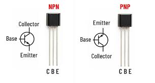
Image taken from : Transistor
Transistors are made of semiconductors, usually silicon. They are:
- Much smaller than vacuum tubes
- More reliable and energy-efficient
- Cheaper to produce
Transistors completely changed electronics. Radios, computers, and many other devices became smaller, faster, and more practical. Today, billions of transistors fit on a single tiny chip.
3. Integrated Circuits (ICs)
By the 1960s, engineers realized that connecting lots of transistors together on a circuit board was still bulky and complicated. The solution was the Integrated Circuit (IC):
- Many transistors, resistors, and capacitors built on a single small silicon chip
- Made electronics smaller, faster, and cheaper
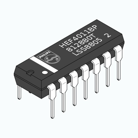
Image taken from : Integrated Circuit | IC Definition, Types & Advantages
ICs are used in almost every electronic device today. For example:
- Microchips in computers and smartphones
- Embedded controllers in washing machines or cars
- Memory chips for storing data
Thanks to ICs, devices that once filled entire rooms could now fit in your pocket.
4. Levels of Integration in Integrated Circuits
As semiconductor fabrication technology improved, engineers were able to place increasing numbers of transistors onto a single silicon chip. The classification of ICs is based on the approximate number of transistors integrated into one chip.
The levels of integration are defined as follows:
SSI – Small Scale Integration
Transistor Count: Fewer than 100 transistors per chip
- Typically 10–100 transistors
- Used for basic logic gates (AND, OR, NOT, NAND, NOR)
- Required many ICs to build complete systems
MSI – Medium Scale Integration
Transistor Count: 100 to 3,000 transistors per chip
- Used for counters, registers, multiplexers, and small arithmetic circuits
- Reduced circuit complexity compared to SSI designs
LSI – Large Scale Integration
Transistor Count: 3,000 to 100,000 transistors per chip
- Enabled early microprocessors and memory chips
- Allowed major functional blocks of a computer on a single chip
VLSI – Very Large Scale Integration
Transistor Count: 100,000 to 10 million transistors per chip
- Enabled full microprocessors on one chip
- Used in personal computers and early smartphones
- Marked the beginning of modern computing power
ULSI – Ultra Large Scale Integration
Transistor Count: More than 10 million transistors per chip
- Modern processors contain billions of transistors
- Used in CPUs, GPUs, AI accelerators, and advanced mobile processors
- Built using nanometer-scale fabrication technology
Each step made electronics smaller, faster, cheaper, and more reliable. Today, electronics are everywhere, from your phone to cars, drones, and smart homes.
Embedded Microcontroller Simulation
Embedded microcontroller simulation is the process of testing and running a microcontroller-based system in a virtual environment before building the physical hardware. It allows designers to verify circuit connections, program behavior, and overall system functionality without using real components.
Wokwi
The objective of this task was to simulate and test a microcontroller circuit using an online simulator before building it on physical hardware. Instead of directly connecting components on a real board, I first verified the circuit design and program behavior in a virtual environment to reduce errors and avoid damaging components.
For this purpose, I used the Wokwi Online Simulator.
Creating a New Project
Next, I created a new project in the simulator. I first clicked on the Profile section and navigated to My Projects. From there, I selected the New Project option to start a fresh design. I then chose the Raspberry Pi Pico board from the available hardware options and selected Arduino as the programming environment. This set up a new workspace with the required board and code editor ready for development.
Understanding the Setup
After creating the project, the simulator automatically generated:
- A Raspberry Pi Pico board
- A default Arduino sketch file
- A simulation environment with wiring view
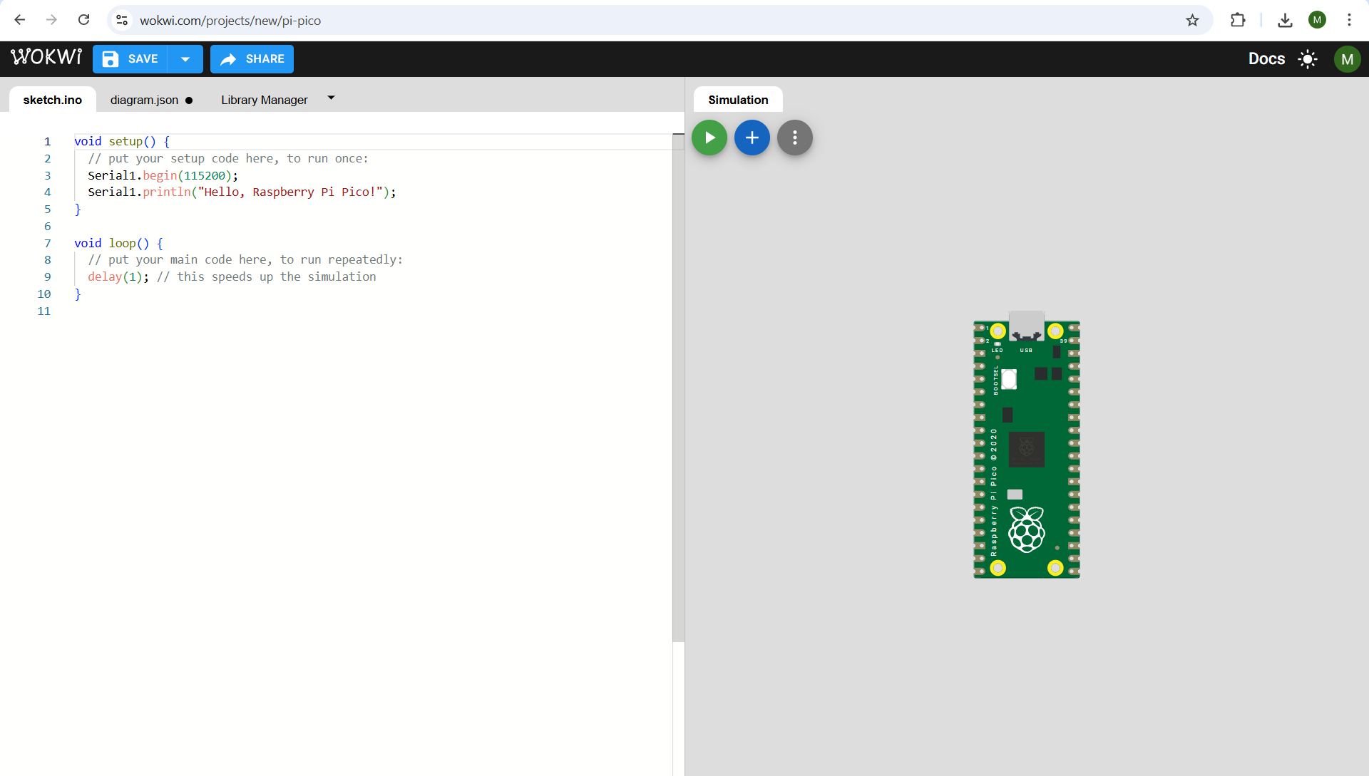
Writing the Code
I modified the default Arduino code to test basic functionality such as blinking an LED.
            void setup() {
                pinMode(5, OUTPUT); // Built-in LED pin for Raspberry Pi Pico
            }

            void loop() {
                digitalWrite(5, HIGH);
                delay(1000);
                digitalWrite(5, LOW);
                delay(1000);
            }
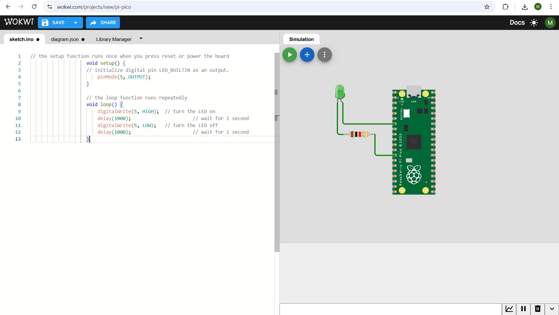
I clicked the Start Simulation button. The built-in LED connected to GPIO 5 started blinking, confirming that the code was working correctly.
Observation
The simulation successfully demonstrated the basic operation of the Raspberry Pi Pico using Arduino code. The LED blinked at a 1000 ms interval, confirming correct pin configuration and program execution.
Learning Outcome
- Understood how to create a new microcontroller project in Wokwi.
- Learned how to simulate Raspberry Pi Pico using Arduino framework.
- Verified code functionality before physical implementation.
- Understood GPIO pin control and timing using delay().
Conclusion
Using Wokwi allowed me to safely test and debug my microcontroller code without requiring physical hardware. This helps reduce errors before implementing the design in a real embedded system.
Pushbutton with OLED
Objective
To interface a pushbutton and an OLED display with a Raspberry Pi Pico and display different messages on the screen depending on the button state.
Components Used
- Raspberry Pi Pico
- Pushbutton
- SSD1306 128x64 I2C OLED display
- Connecting wires
- Wokwi simulator
Working Principle
The pushbutton is configured as a digital input using the INPUT_PULLUP mode. In this configuration:
- The input pin remains HIGH by default.
- When the button is pressed, the pin connects to GND.
- The pin then reads LOW.
The OLED display communicates with the Raspberry Pi Pico using the I2C communication protocol. The program continuously reads the button state. If the button is pressed, a specific message is displayed on the OLED. If the button is not pressed, a different message is displayed.
Circuit Connections
Pushbutton Connections
One terminal of the pushbutton is connected to GPIO 2.
The other terminal is connected to GND.
No external resistor is required because the internal pull-up resistor is enabled in the program.
OLED Display Connections (I2C)
| OLED Pin | Connected To Pico |
|---|---|
| VCC | 3.3V |
| GND | GND |
| SDA | GPIO 4 |
| SCL | GPIO 5 |
Program Code
            #include <Arduino.h>
            #include <U8g2lib.h>
            #include <Wire.h>

            U8G2_SSD1306_128X64_NONAME_F_HW_I2C u8g2(U8G2_R0, U8X8_PIN_NONE);

            const int buttonPin = 2;

            void setup() {
                pinMode(buttonPin, INPUT_PULLUP);
                u8g2.begin();
            }

            void loop() {
                int buttonState = digitalRead(buttonPin);

                u8g2.clearBuffer();
                u8g2.setFont(u8g2_font_ncenB08_tr);

                if (buttonState == LOW) {
                    u8g2.drawStr(0, 30, "Button Pressed!");
                }
                else {
                    u8g2.drawStr(0, 30, "Press the Button");
                }

                u8g2.sendBuffer();
                }
Code Explanation
In the setup function, the button pin is configured as INPUT_PULLUP and the OLED display is initialized using the U8g2 library.
In the loop function, the program reads the button state. The display buffer is cleared before writing new content. If the button is pressed (LOW), the display shows "Button Pressed!". If the button is not pressed (HIGH), the display shows "Press the Button". The buffer is then sent to the display.
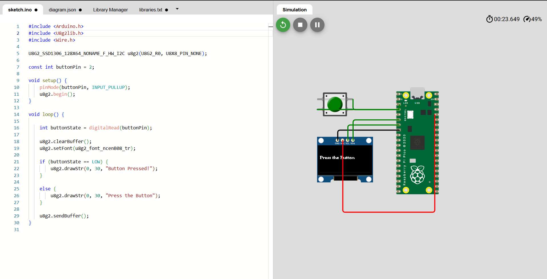
Expected Result
When the button is not pressed, the OLED displays:
Press the Button
When the button is pressed, the OLED displays:
Button Pressed!
Electronic Design
KiCad
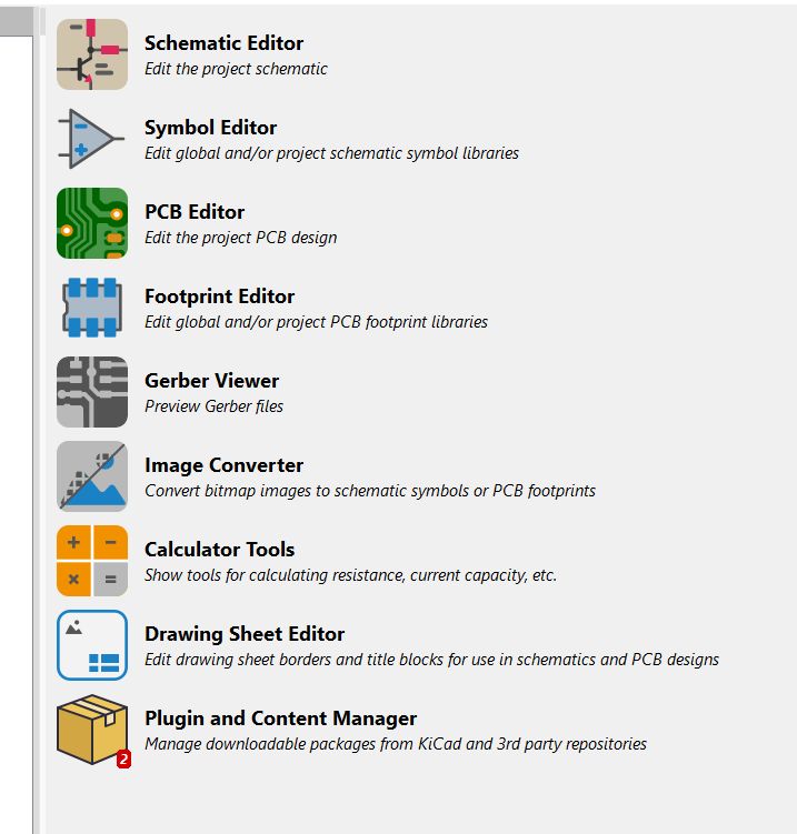
KiCad is a free and open-source Electronic Design Automation (EDA) software suite used for designing electronic schematics and printed circuit boards (PCBs).
The software includes several integrated tools, such as:
1. Schematic Editor
Used to create and edit the project schematic. This is where circuit diagrams are drawn by placing symbols and connecting them with wires.
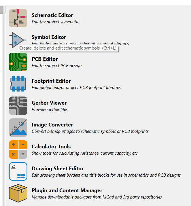
2. Symbol Editor
Used to create, modify, and manage schematic symbols. It allows editing of global or project-specific symbol libraries.
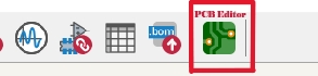
3. PCB Editor
Used to design the printed circuit board layout. Components are placed on the board and connected using copper tracks.
4. Footprint Editor
Used to create and edit PCB footprints. Footprints define the physical pad layout of components on the board.
5. Gerber Viewer
Used to open and preview Gerber files. This helps verify manufacturing files before sending them to a PCB fabrication service.
6. Image Converter
Used to convert bitmap images into schematic symbols or PCB footprints. This is helpful for adding logos or custom graphics to a design.
7. Calculator Tools
Provides electrical calculation tools such as resistor value calculators, track width calculators, and other design-related utilities.
8. Drawing Sheet Editor
Used to edit the drawing sheet format, including borders and title blocks, for schematic and PCB documents.
9. Plugin and Content Manager
Used to manage downloadable libraries, plugins, and external content from KiCad and third-party repositories.
Create a New Project
- Click File in the top left corner.
- Select New Project.
- Choose the folder where you want to save your project.
- Enter your project name.
- Click Save.
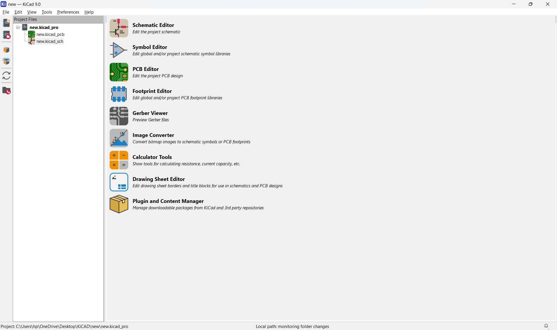
When a new project is created in KiCad, the software automatically generates several important files. Each file serves a specific purpose in the design process.
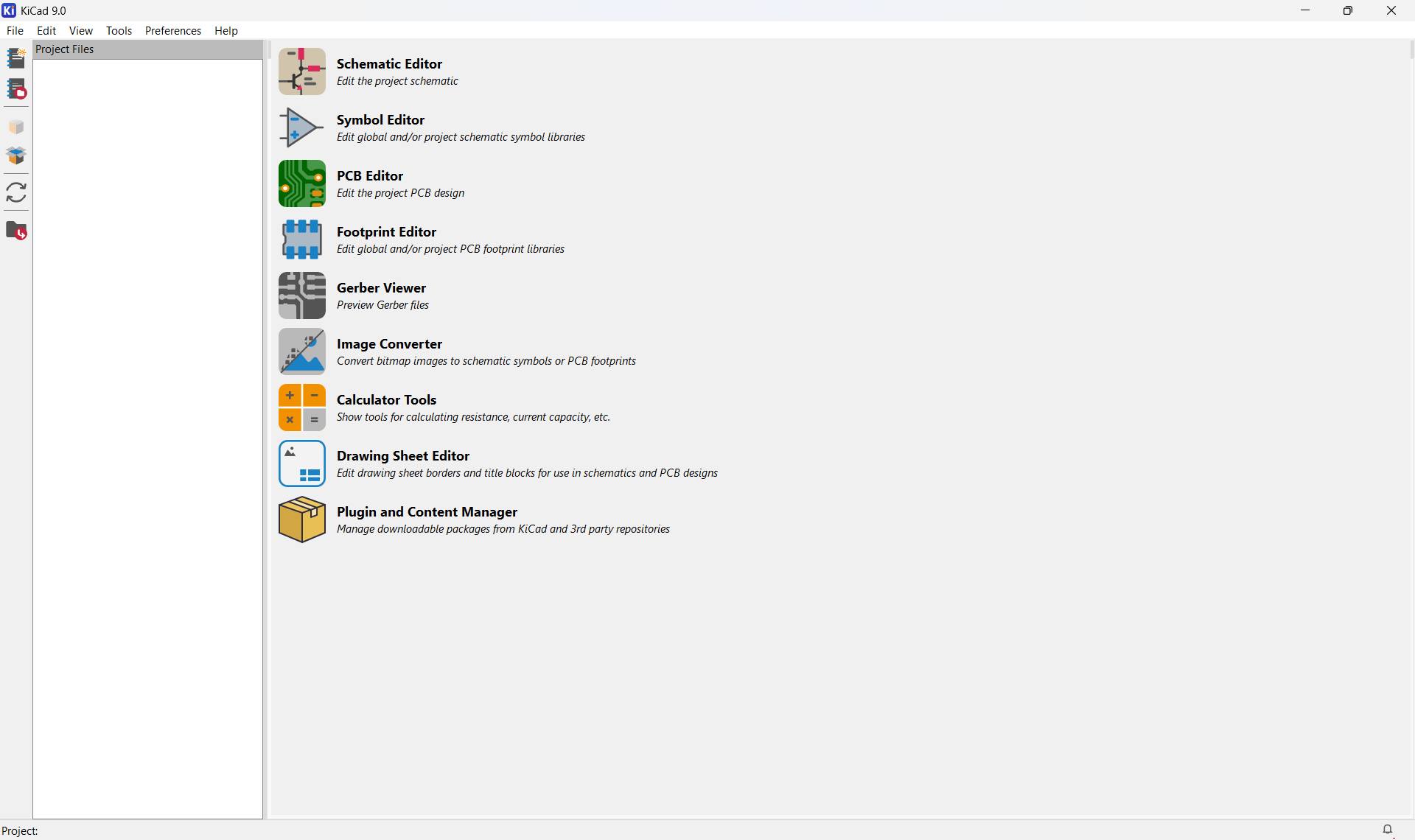
Kicad Project Manager
The KiCad Project Manager is the main control window that appears when you open a KiCad project. It acts as the central hub for managing all files and tools related to a specific electronic design project.
In the Project Manager window, locate the Schematic Editor icon, and click it to open the Schematic Editor.
Schematic Editor (Eeschema)
To begin designing the circuit, the Schematic Editor must be opened from the KiCad Project Manager.
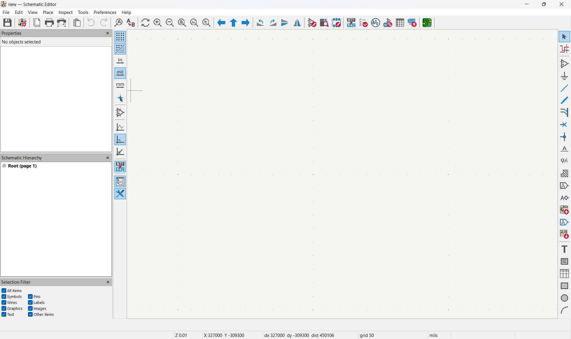
When you open Eeschema, a new window appears with a blank schematic sheet. You will see options such as Add Components, Place Wire, Net Label, and other tools.
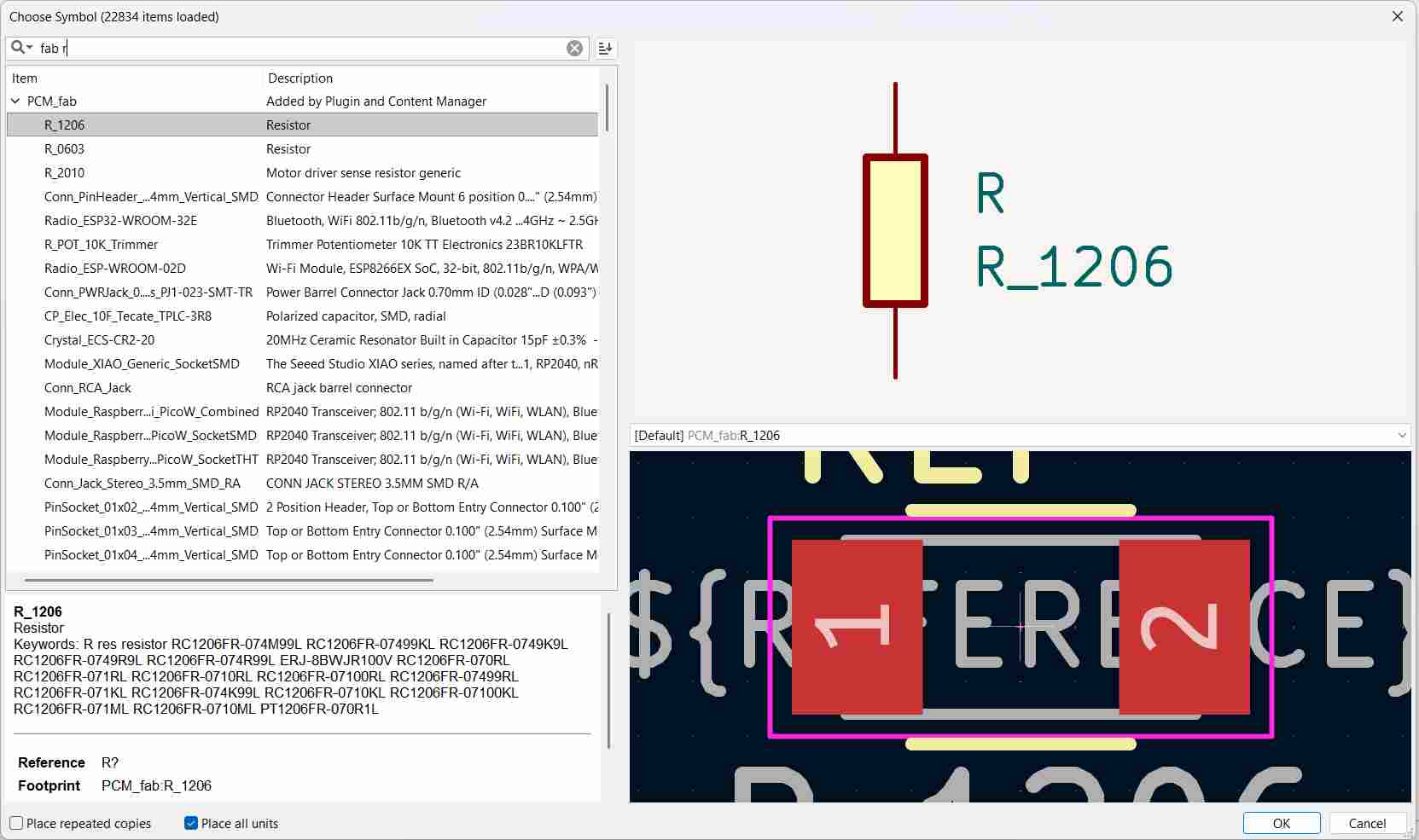
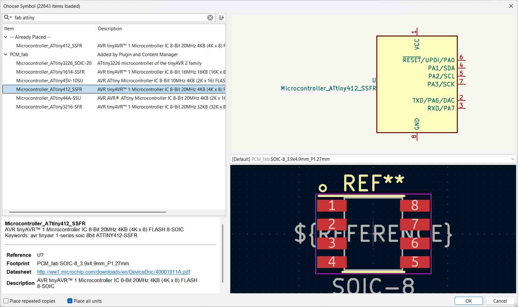
Add Components
- Press A on your keyboard.
- Or click the Add Symbol icon in the right toolbar.
A window called Choose Symbol will open. On the left side, you will see different libraries. On the right side, you will see the available components (symbols) from the selected library.
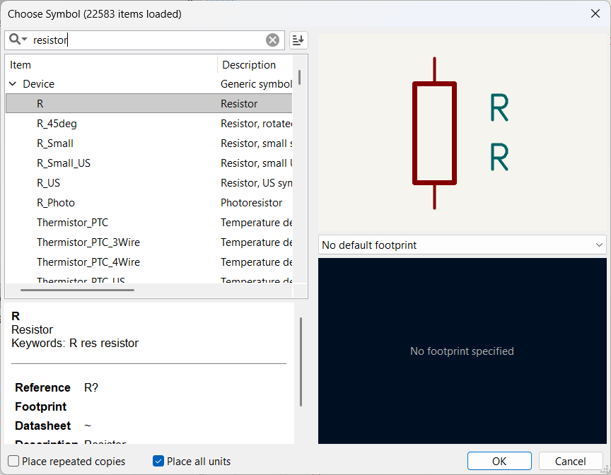
Use the search bar at the top of the Choose Symbol window.
You can further filter the results by using keywords or by selecting a specific library name.
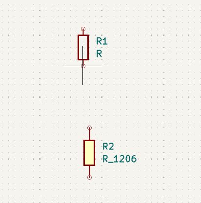
- Type the component name:
- R → Resistor
- C → Capacitor
- D → Diode
- LED → Light Emitting Diode
- GND → Ground
- Microcontroller name (example: ATtiny, STM32, etc.)
- You can filter by keyword or library name.
Click on a symbol to see its preview. Check the pin count, pin names, and symbol type to ensure it matches your requirement. After verifying the details, click OK to select the symbol.
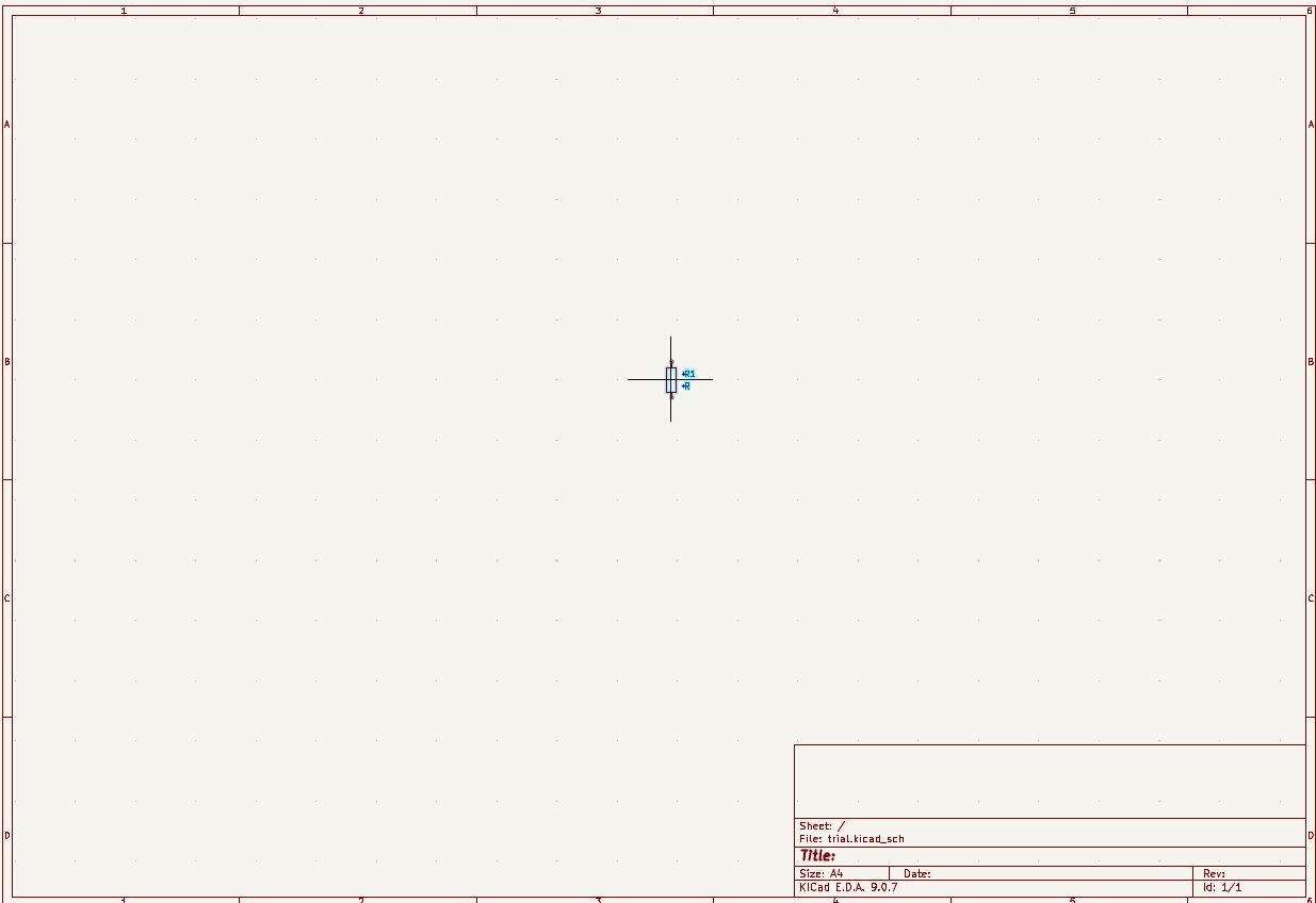
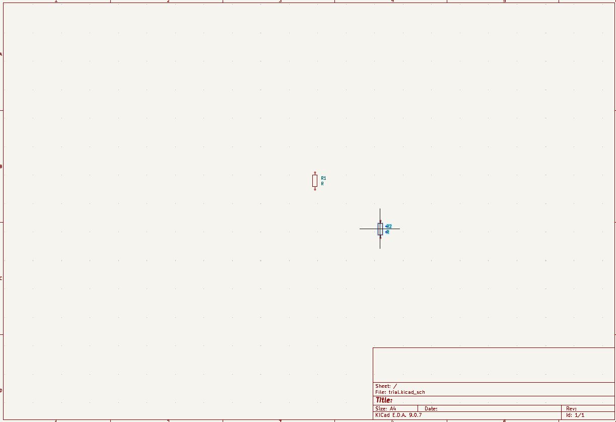
Move your cursor to the schematic sheet and left click to place the component. You can place multiple copies by clicking again at different locations. Press Esc to stop placing the component.
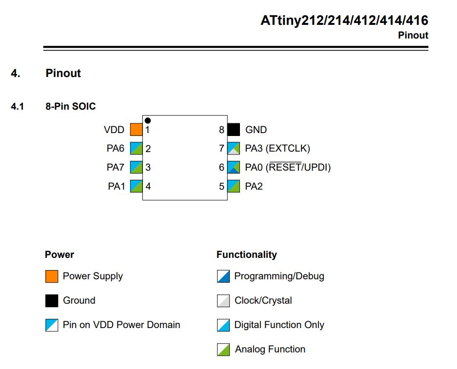
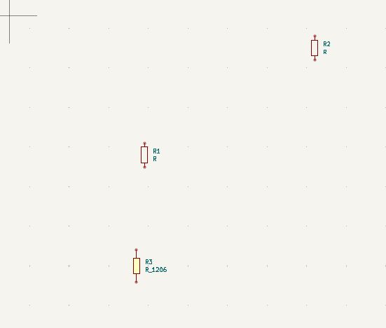
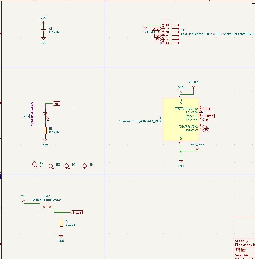
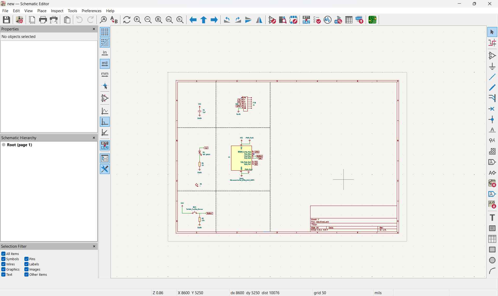
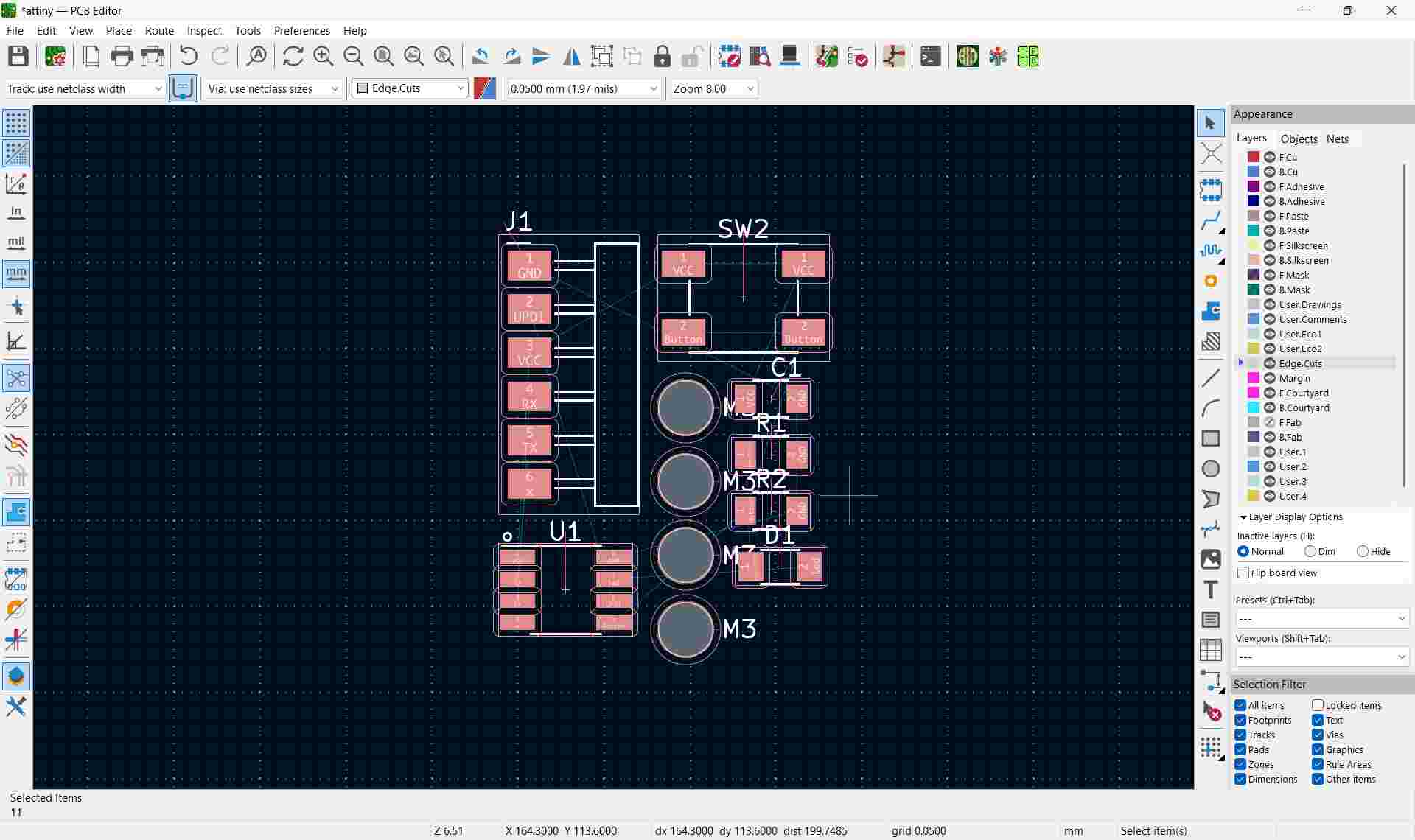
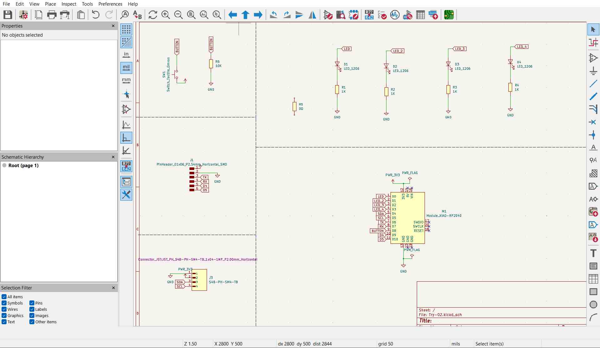
We decided to recreate the ATtiny412 Blink board from the Embedded Programming week, made by Neil. Working from that reference schematic, I recreated the circuit in KiCad using components sourced from the Fab library.
KiCad Library Management
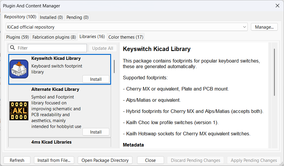
To streamline the design process and ensure access to common mechanical and electrical components, I utilized the KiCad Plugin and Content Manager.
Installing KiCad FabLib
Make sure you have KiCad 8 or later installed before proceeding with the installation.
Go to:
Tools → Plugin and Content Manager
or press:
Ctrl + M
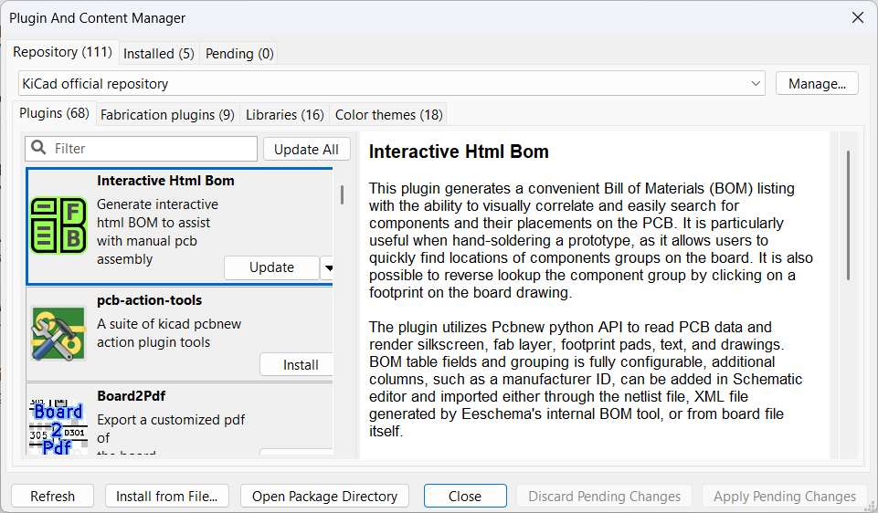
Click on the Libraries tab.
Look for "KiCad FabLib" in the list of available libraries under the Libraries tab.
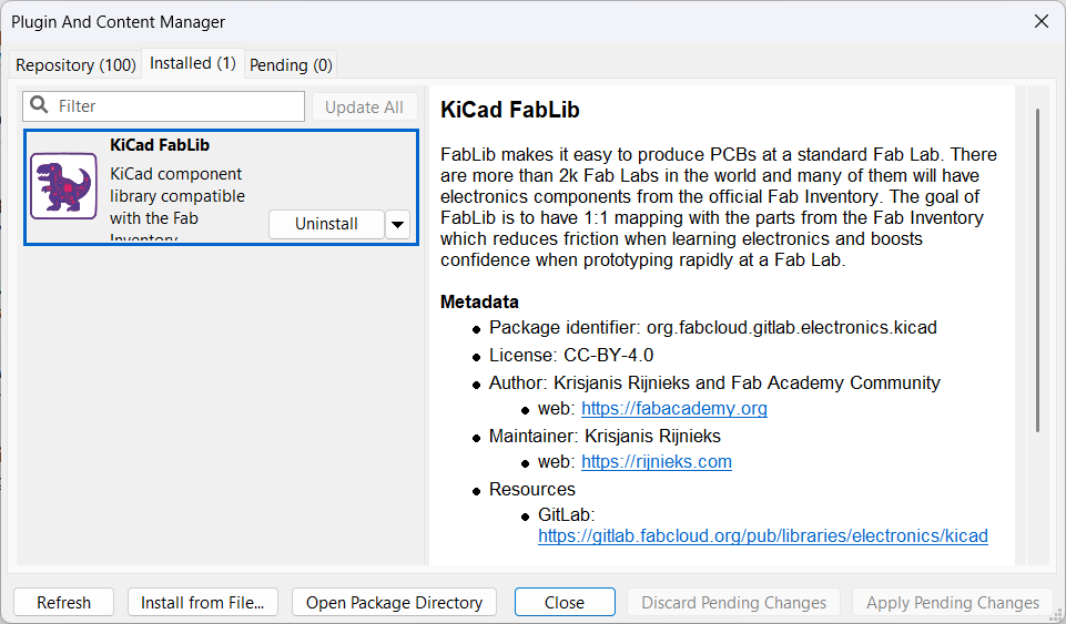
Click the Install button next to KiCad FabLib.
After installation, click Apply Pending Changes to complete the process.
When searching for components in the schematic or PCB editor, installed fab library components appear with the prefix fab in the search results.
So I imported the needed components from the Fablab library.
Rotating and Flipping Before Placement
- Press R to rotate 90°.
- Press X to flip horizontally.
- Press Y to flip vertically.
Adding Values to Symbols
Think of the Value as the price tag on a component. It tells you what that component is. For example, a resistor worth 10k ohms, a capacitor of 100nF, or a chip called AMS1117-3.3. Without a value, the symbol is just a shape with no meaning.
Method 1 — Double-click the symbol
- Place the symbol on the schematic.
- Double-click it to open the Symbol Properties dialog.
- Find the Value row in the fields table.
- Click the cell in the Value column and type the component value (example: 10k, 100nF, 2N2222).
- Click OK to apply.
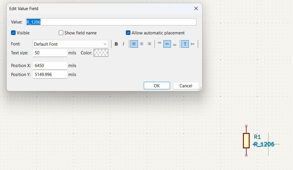
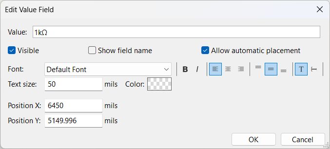
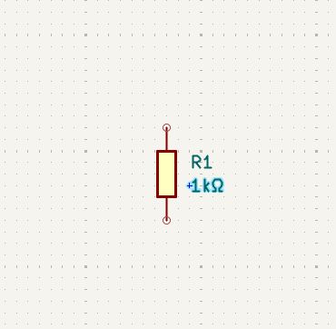
Method 2 — Double-click the value text directly
- On the schematic, find the value text sitting below or beside the symbol (it shows the current value, for example R or C by default).
- Double-click that text label.
- A small edit box appears — type the new value directly.
- Press Enter to confirm.
Method 3 — Press E with the symbol selected
- Single-click the symbol to select it.
- Press E on the keyboard.
- The Symbol Properties dialog opens — edit the Value field.
- Click OK.
Editing Other Component Properties
- Double-click the placed component.
- Edit:
- Reference (Example: R1, C1)
- Value (Example: 10k, 100nF)
- Footprint (Important for PCB design)
- Datasheet link (optional)
What is a Footprint?
A footprint defines the physical layout of a component on the PCB. It includes pad size, pad spacing, drill holes, and overall package shape. The schematic symbol and PCB footprint are separate and must be linked.
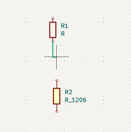
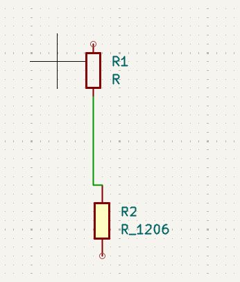
Wiring and Electrical Checks
Add Wires
- Press W.
- Click from one pin to another.
- Press Esc to stop wiring.
We added the ATtiny412 directly from the fab library.
We added a push button to the circuit.
Global Labels
A Global Label is like a name tag you stick on a wire. If two pins have the same name tag, KiCad treats them as connected even if they are far apart or on completely different schematic sheets. No wire needs to be drawn between them.
How to place a Global Label:
- Move your cursor to the pin or wire end where you want to attach the label.
- Press Ctrl + L, or go to Place Global Label in the rightmost toolbar.
- In the dialog that appears, type the label name (example: SDA, VCC, UART_TX).
- Choose the Connection Type:
- Input — signal enters this component through this pin.
- Output — signal leaves this component through this pin.
- Bidirectional — signal can travel in either direction (common for data lines).
- Tri-state — pin can be driven high, low, or left floating.
- Passive — direction is not specified (use for power or generic nets).
- Click OK.
- Click at the exact end of a pin or wire to attach the label. The label must snap to a pin or wire endpoint — a dangling label is flagged as an ERC error.
- Press Esc to stop placing labels.
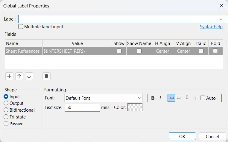
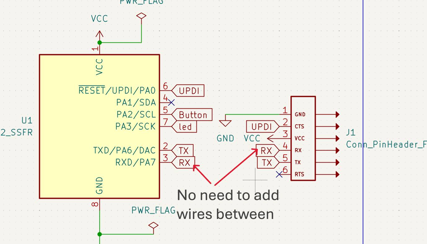
To create the matching connection on another component or sheet, repeat the same steps and type the identical label name. KiCad treats all global labels with the same name as one continuous net.

I used this website to calculate the resistor value for the LED: LED Resistor Calculator
Run Electrical Rules Check (ERC)
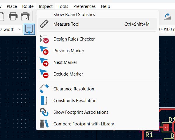
Click on ERC in the top toolbar or go to Inspect → Electrical Rules Checker.
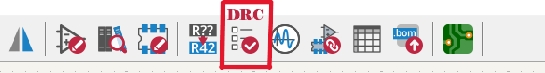
In the ERC window, click Run to analyze the schematic for electrical issues.
Review all reported errors and warnings. Double-click on each issue to locate it in the schematic and correct the problem.
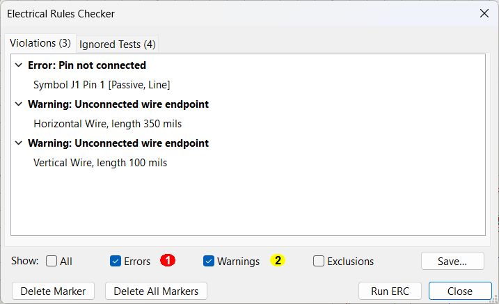
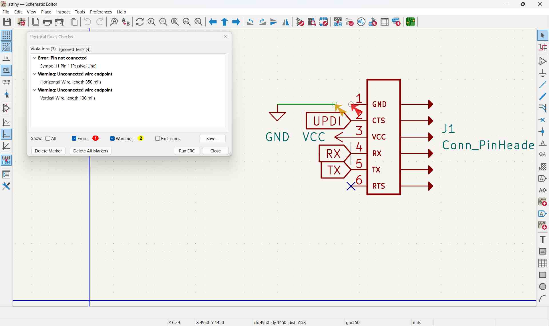
Repeat the process until no unresolved errors or critical warnings remain.
PCB Design
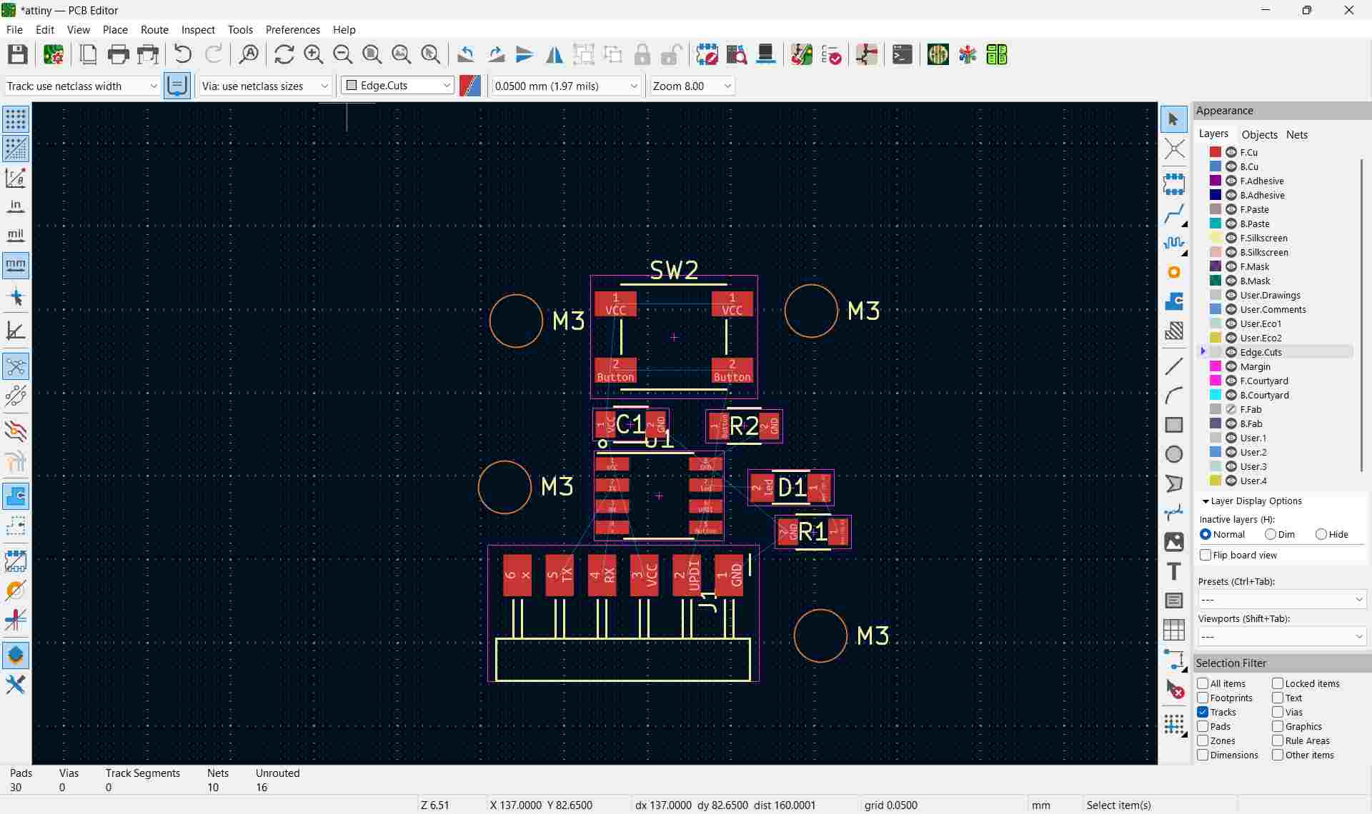
Once the schematic is verified, open the PCB Editor from the KiCad Project Manager by clicking on PCB Editor.
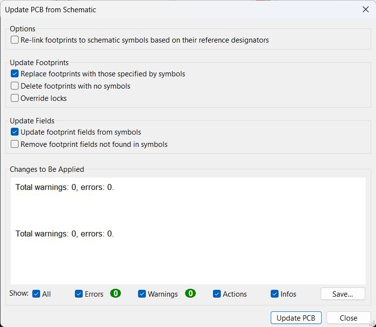
To transfer the design from the schematic to the PCB layout, return to the Schematic Editor and select Tools → Update PCB from Schematic. In the update window that appears, click Update PCB.

PCB Trace (Routing Tracks) in KiCad
A PCB trace is a copper path that electrically connects component pads on the PCB. It replaces the wires from your schematic.
- Update PCB from schematic.
- Arrange all component footprints properly.
- Set proper track width (based on current requirements).
To do this, you can click and drag them to the desired positions.
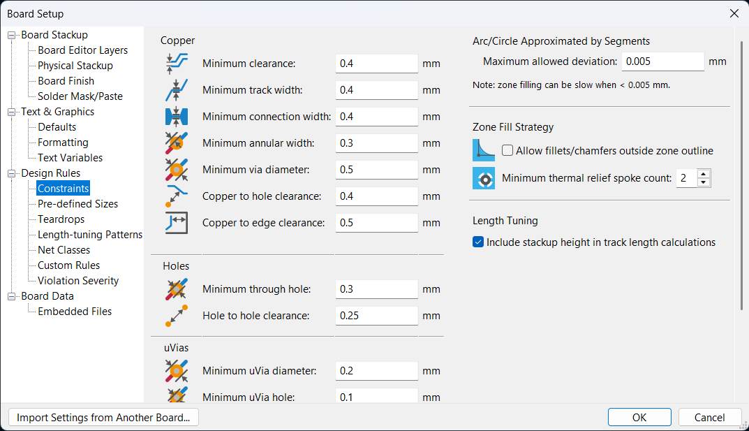
Setting Constraints in the PCB Editor
Constraints tell KiCad the rules your board must follow. Things like how thick a copper track must be, how much space to leave between tracks, and how large drill holes should be. Getting these right before you start routing saves you from having to redo everything later.
Go to File → Board Setup (or press Ctrl + Shift + P).

This opens the Board Setup window. The constraints you need are under Design Rules → Constraints in the left sidebar.
- Minimum track width — the thinnest a copper track can be. For PCB milling in a Fab Lab, use 0.4 mm or wider. Thinner tracks break easily when milled.
- Minimum clearance — the smallest gap allowed between any two copper shapes. Use 0.4 mm for milling; commercial fabs can go as low as 0.1 mm.
- Minimum annular width — the ring of copper around a drill hole. A value of 0.3 mm is a safe minimum.
- Copper to edge clearance — how far copper must stay from the board edge. Use at least 0.5 mm to avoid shorts during milling.
How to set a constraint
- Find the constraint you want to change (e.g. Minimum track width).
- Click the value next to it and type your new number.
- Click OK to save and close.
Routing Traces
Step 1: Select Route Tool
- Open PCB Editor.
- Press X on your keyboard.
- Or click the Route Tracks icon from the right toolbar.

Step 2: Start Routing
Click on the target pad and drag the mouse.
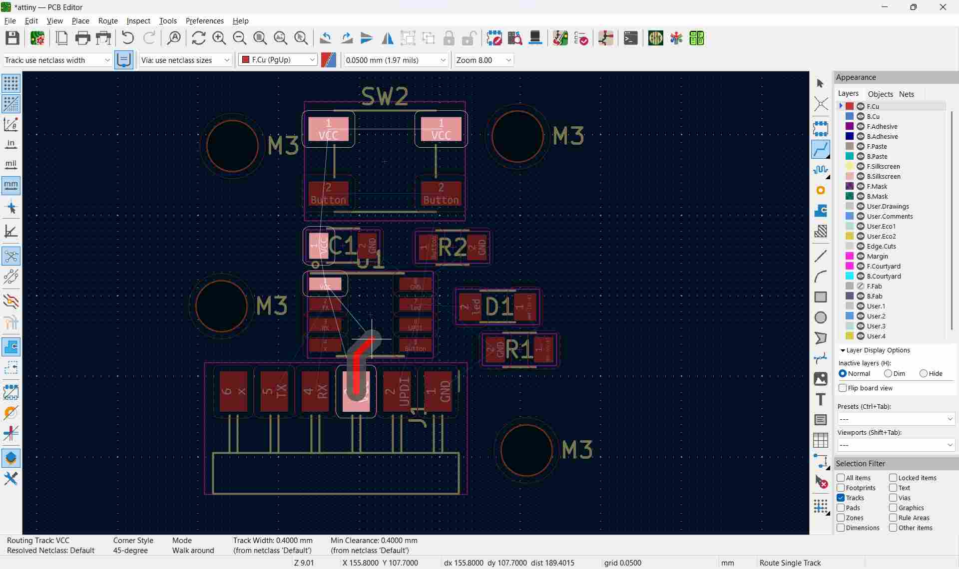
Click again when you reach the destination pad.
- Follow the white ratsnest line as a guide.
Routing Tips
- Keep traces short and clean.
- Avoid sharp angles (use 45° angles).
- Avoid crossing traces on the same layer.
- Maintain proper spacing between tracks.
Deleting a Trace
- Click on the trace.
- Press Delete.
Dragging or Adjusting Trace
- Hover over the trace.
- Press G to drag while keeping connections.
Edge Cut in KiCad PCB Editor
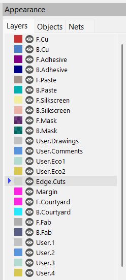
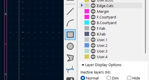
- Select Edge.Cuts layer
- Select 'Draw Rectangle' tool
- Draw board boundary
- Ensure closed shape
Alternative Method: Draw Rectangle Using Lines
- Select Add Graphic Line.
- Click to draw the first edge.
- Draw four lines (top, right, bottom, left).
- Ensure the final line connects exactly to the starting point.
- The shape must be fully closed with no gaps.
Check Design Rules
- Click Inspect → Design Rules Checker (DRC).
- Fix any clearance or connection errors.
The Edge.Cuts layer defines the physical boundary of the PCB. This outline tells the manufacturer where the board should be cut. The shape must always be a fully closed loop.
3D Viewer in KiCad PCB Editor
The 3D Viewer allows you to see your PCB in a realistic 3D model. It helps you check component placement, board shape, and overall design appearance before fabrication.
Step 1: Open PCB Editor
- Open your project.
- Click PCB Editor.
Step 2: Open 3D Viewer
- Click View in the top menu.
- Select 3D Viewer.
- Or press Alt + 3 (shortcut).
A new window will open showing your PCB in 3D.
Basic Controls in 3D Viewer
- Left Mouse Button: Rotate the board.
- Middle Mouse Button: Pan (move view).
- Mouse Scroll: Zoom in/out.
- Right Mouse Button: Context options.
If Components Do Not Appear in 3D
- Footprints may not have 3D models assigned.
- Open footprint properties.
- Assign a 3D model file (.step or .wrl).
Individual Project
Overview
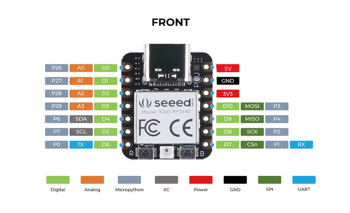
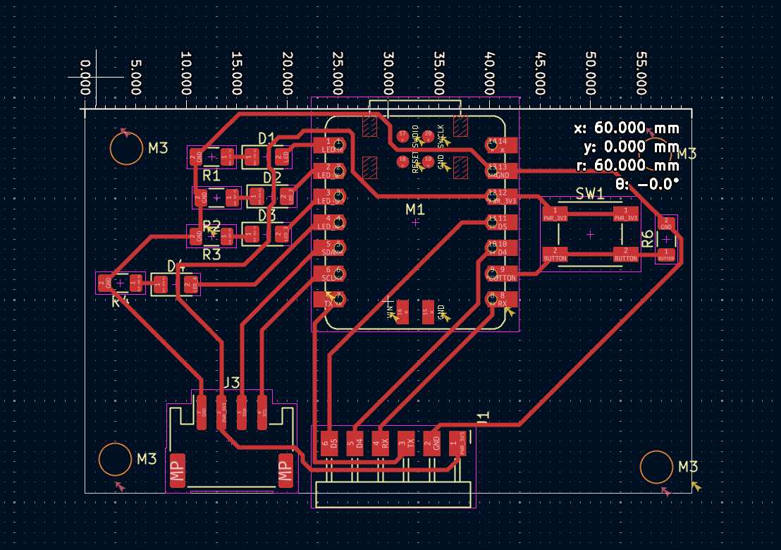
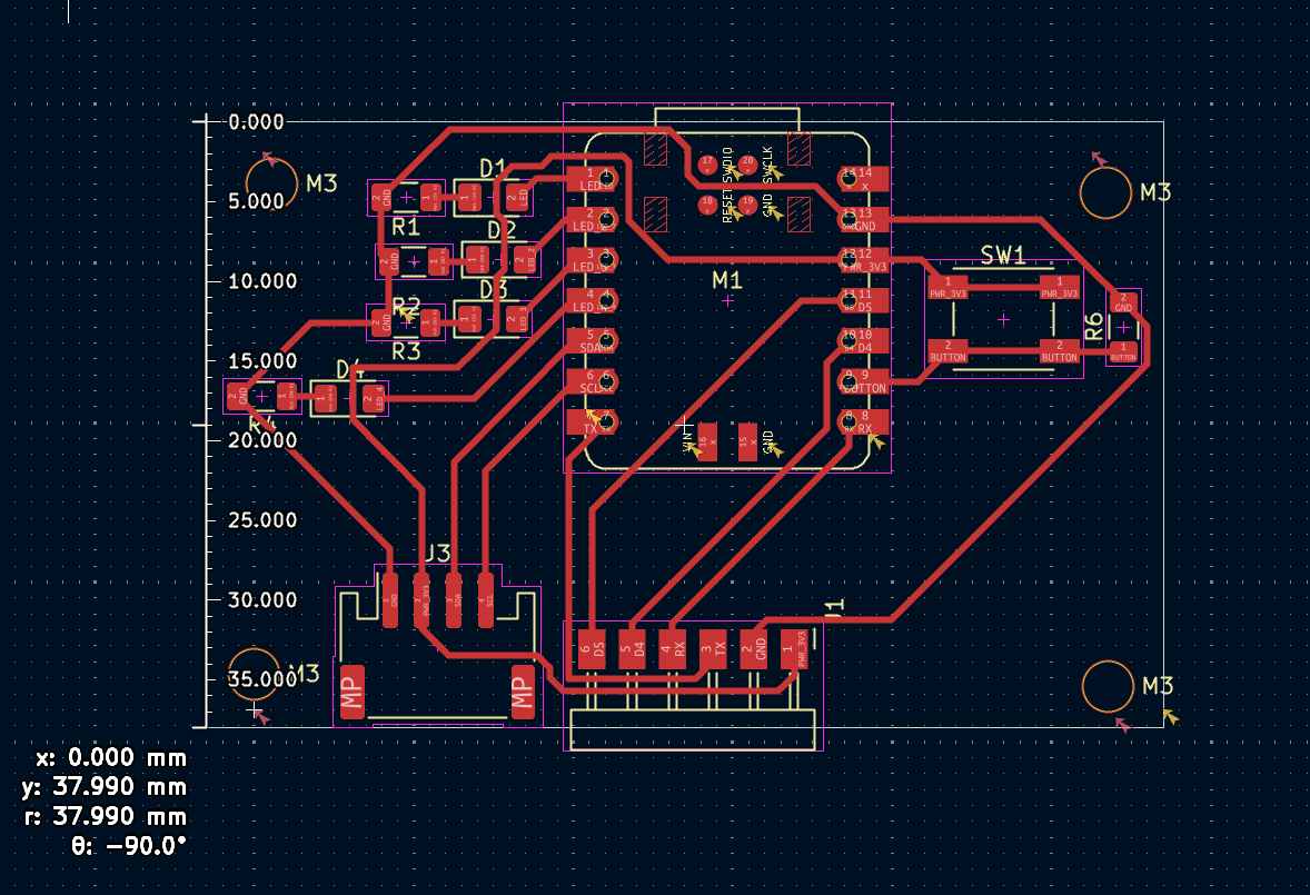
For the individual assignment, I designed a PCB for the LED blinker circuit I had previously built and simulated during the Electronics week. This board was built on Xiao RP2040. The goal was to take that design and turn it into a real, fabrication ready PCB layout using KiCad.
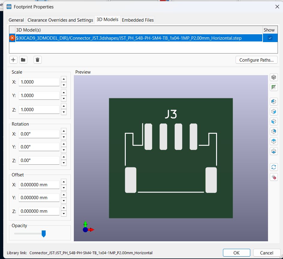
Downloading Additional Components
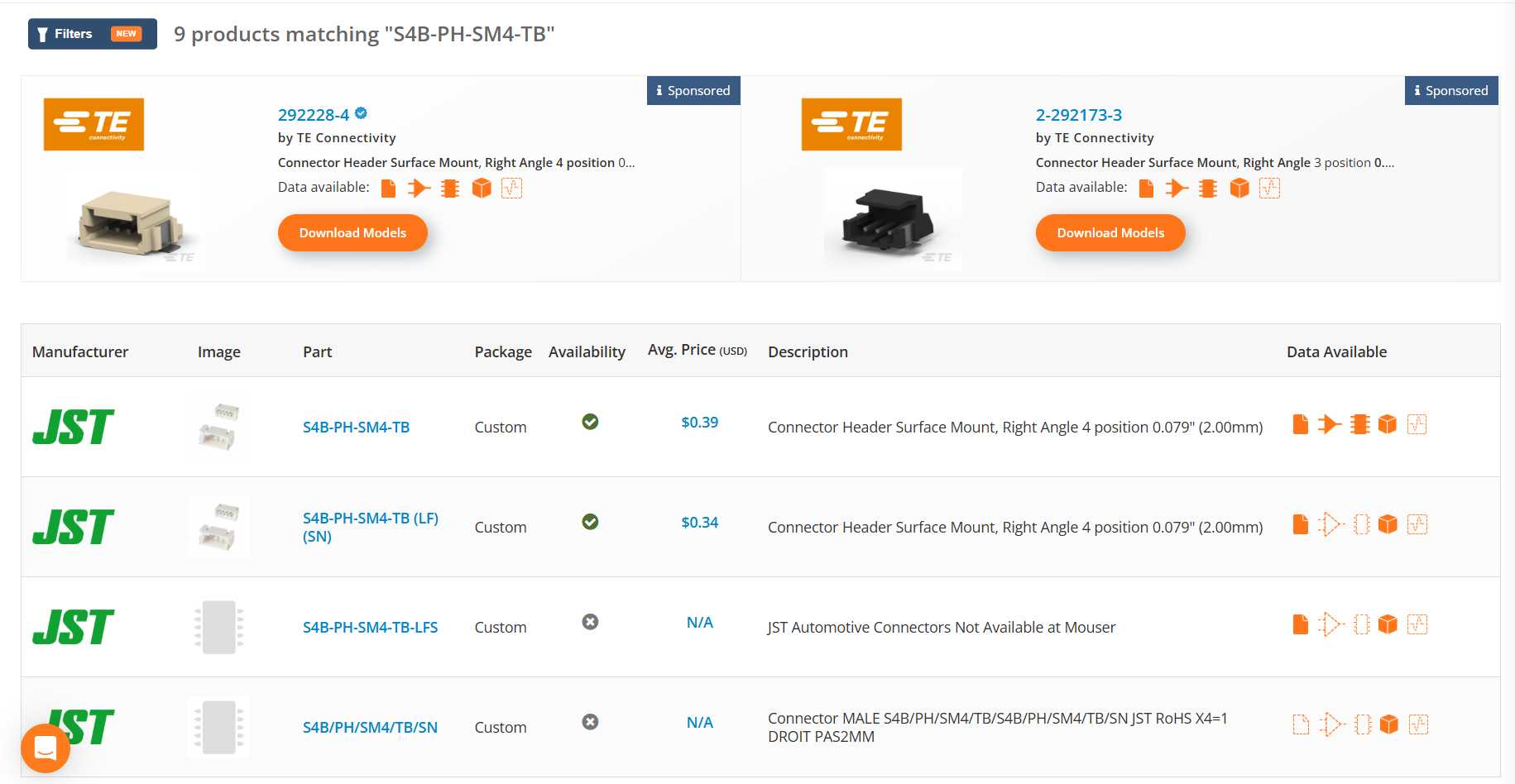
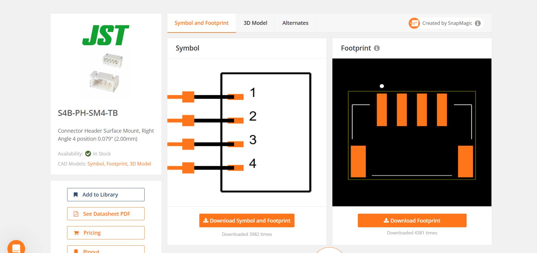
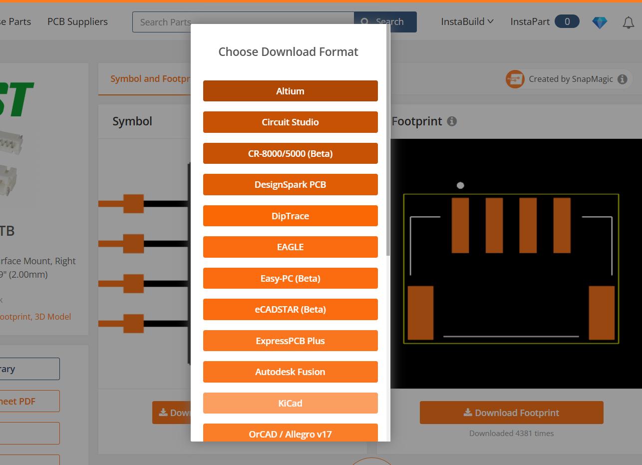
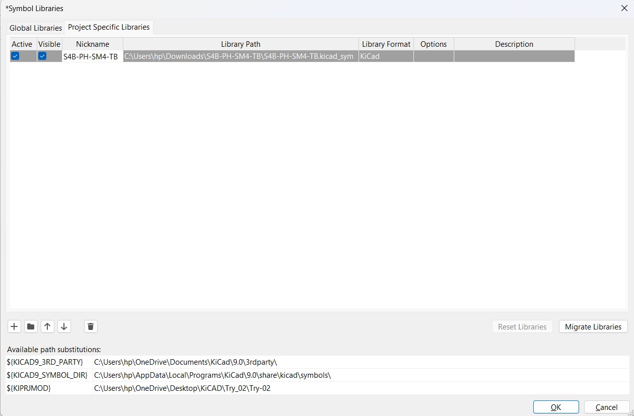
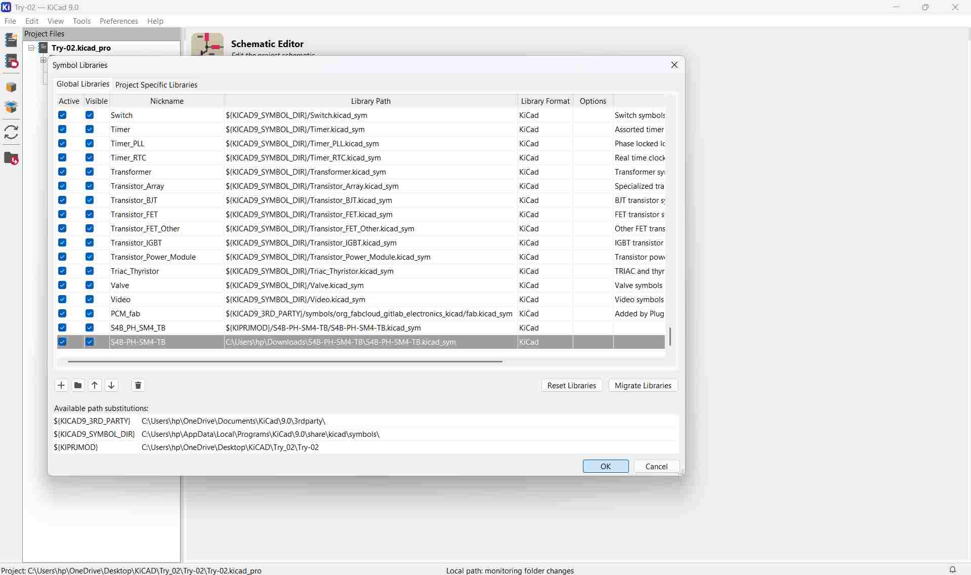
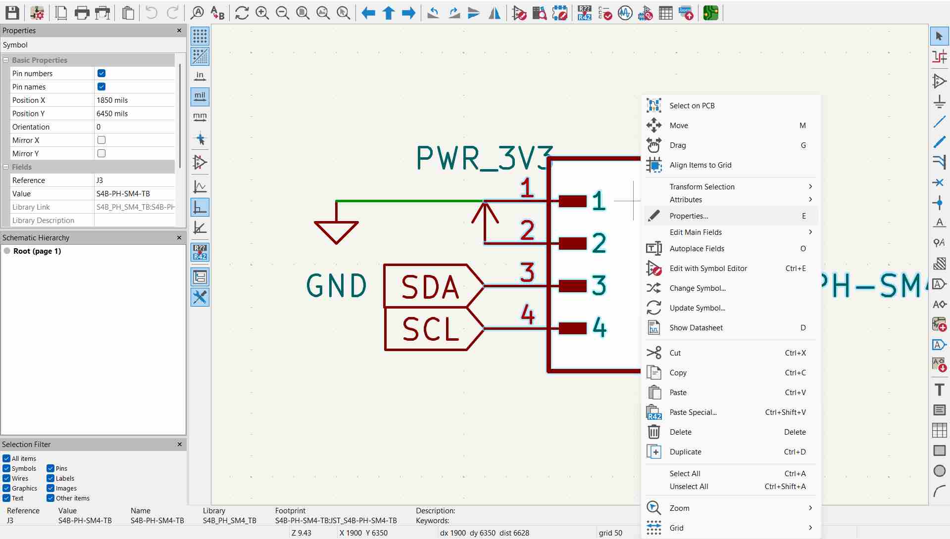
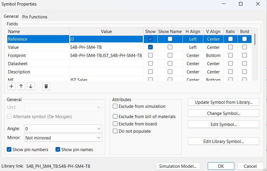
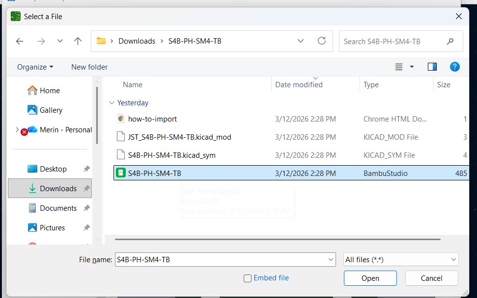
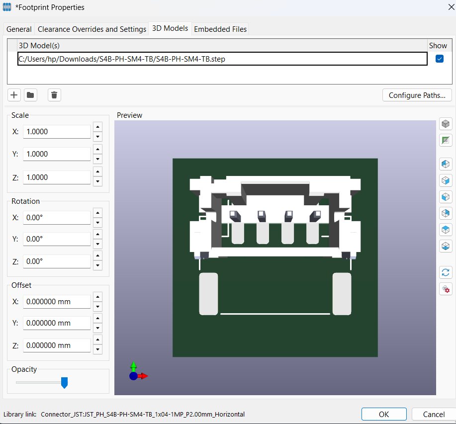
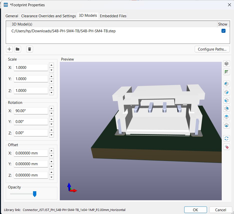
Not all components are available in KiCad's default library. For this project, I needed a S4B-PH-SM4-TB connector, which was not available in KiCad. I downloaded it from SnapMagic, a library of ready-to-use schematic symbols and footprints. This is a useful method whenever a component is missing from KiCad's built-in libraries.

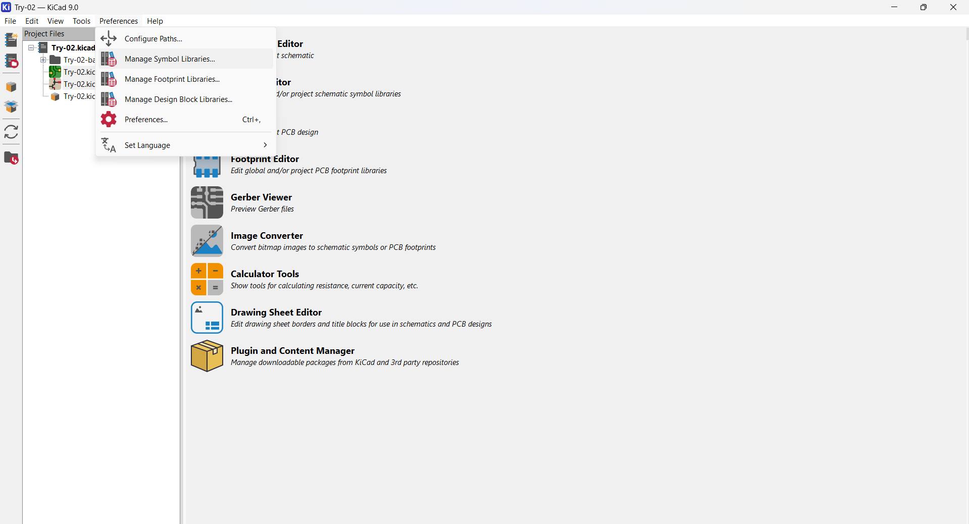
Adding the Component to KiCad
Once downloaded, I imported the component into KiCad by adding it to a local library. The downloaded package includes both the schematic symbol and the PCB footprint, so it can be used directly in the schematic editor and then carried through to the PCB layout.
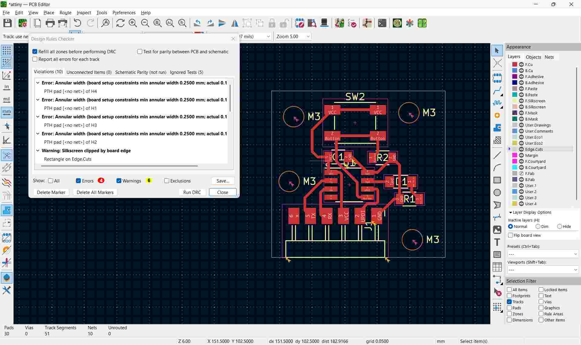
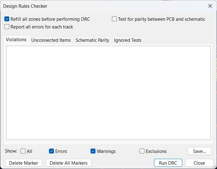
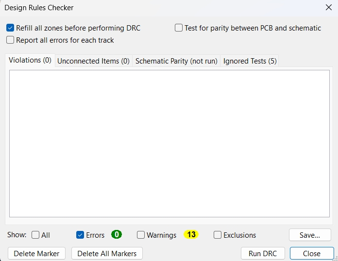
Design Rules Check (DRC)
Once routing was complete, I ran the Design Rules Checker (DRC) in KiCad to do a full automated inspection of the routed board. DRC compares every copper feature, pad, via, and board outline against the constraint values set in the Board Setup, such as minimum trace width (0.4 mm for the Fab Lab Roland MDX milling machine) and minimum clearance between copper objects (0.4 mm). Any violation is flagged with its exact location on the canvas so it can be found and fixed immediately.
The DRC report covered the following checks:
- Clearance violations — two copper features closer than the allowed minimum, which would merge during milling and cause shorts.
- Unconnected nets — pads that the schematic says must be connected but have no routed trace yet.
- Minimum trace width — traces too narrow for the mill bit to cut cleanly without breaking.
- Board outline integrity — missing or overlapping segments in the Edge.Cuts layer that would confuse the milling path.
- Footprint courtyard overlaps — component keep-out areas that overlap, indicating components placed too close to solder cleanly.
After running DRC, I addressed each flagged item, adjusting trace routes or clearances as needed, until the checker reported zero errors. Only then did I proceed to measure board dimensions and export for fabrication.
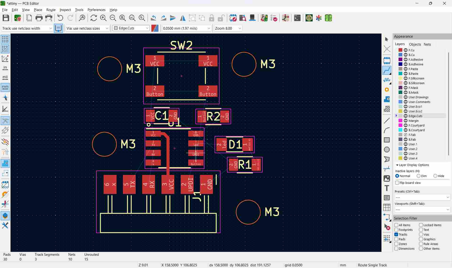
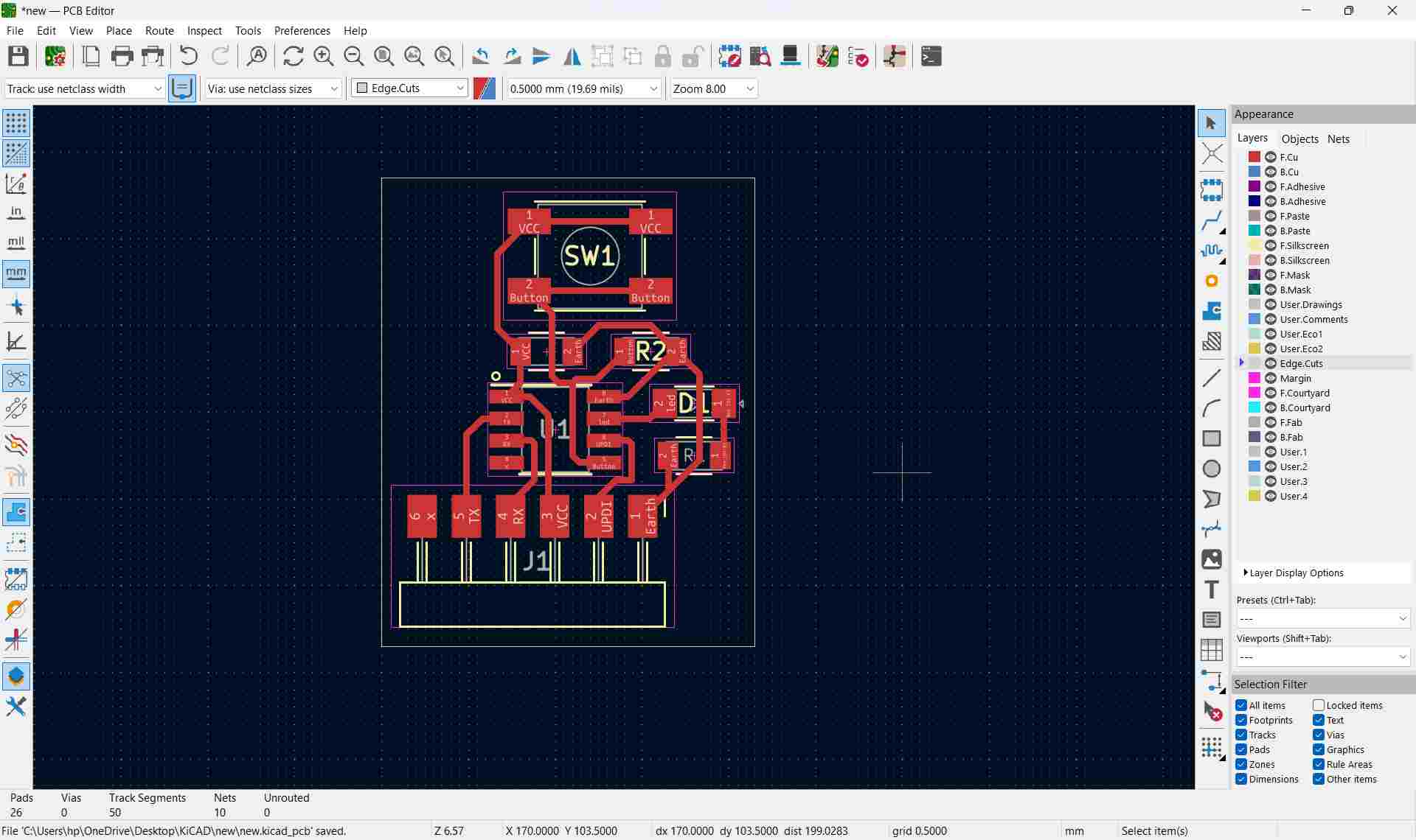
Routing Traces
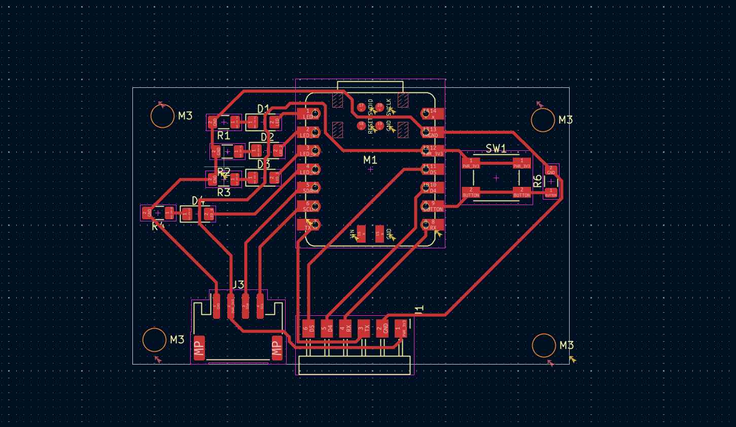
With all components placed in the schematic, I opened the PCB Editor and arranged them within the board outline. I kept the layout compact while maintaining enough clearance between parts for reliable fabrication.
I routed all the copper traces manually, connecting the pads according to the ratsnest (the unconnected net lines from the schematic). I used appropriate trace widths for power and signal lines to ensure the board meets fabrication requirements.
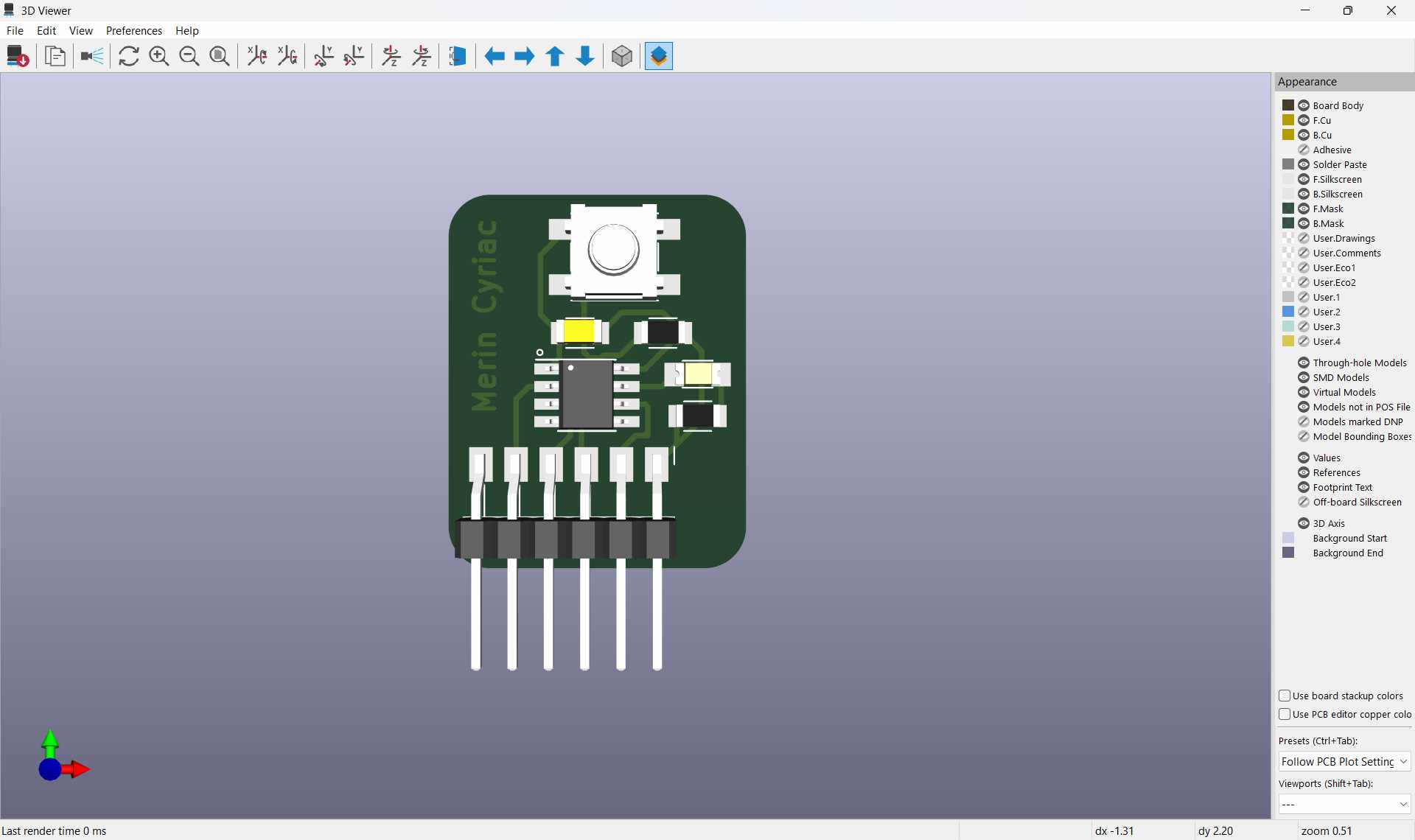
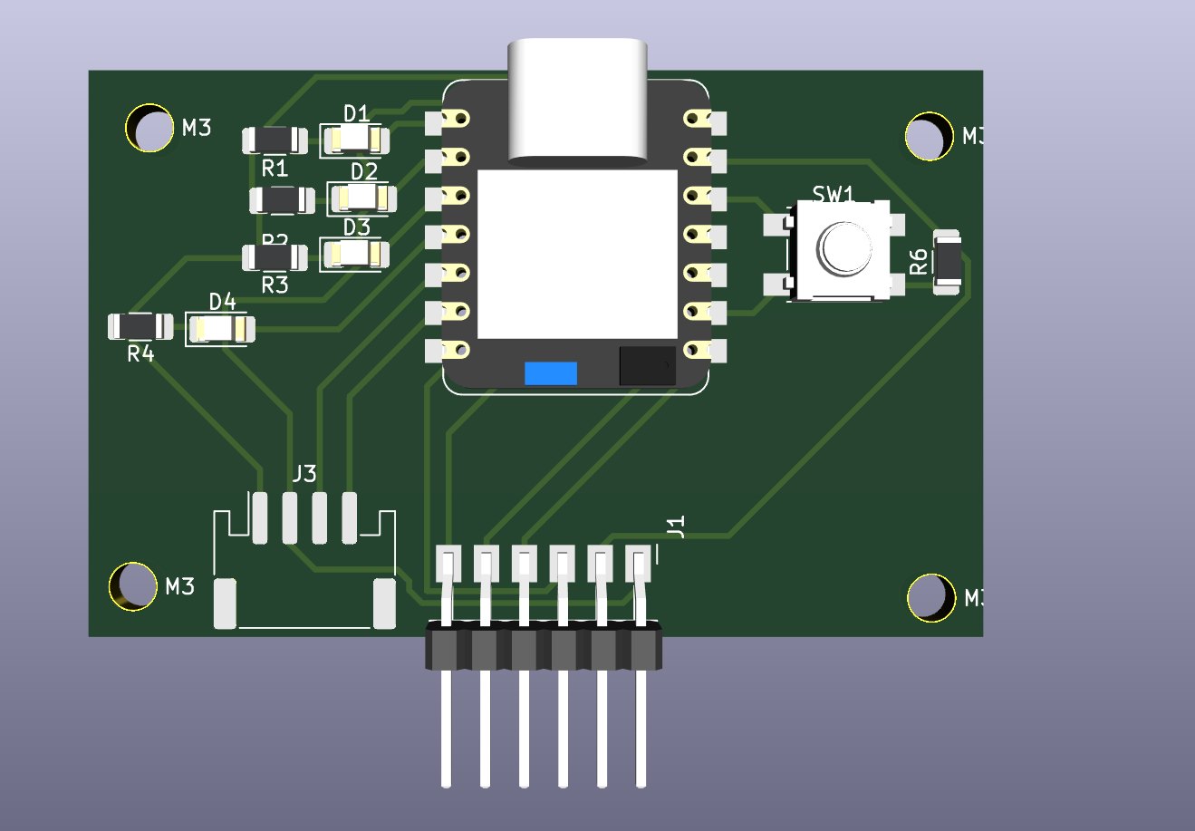
3D Preview
I used KiCad's 3D Viewer to do a final visual check of the board — confirming component placement, orientation, and the overall footprint of the design before exporting.
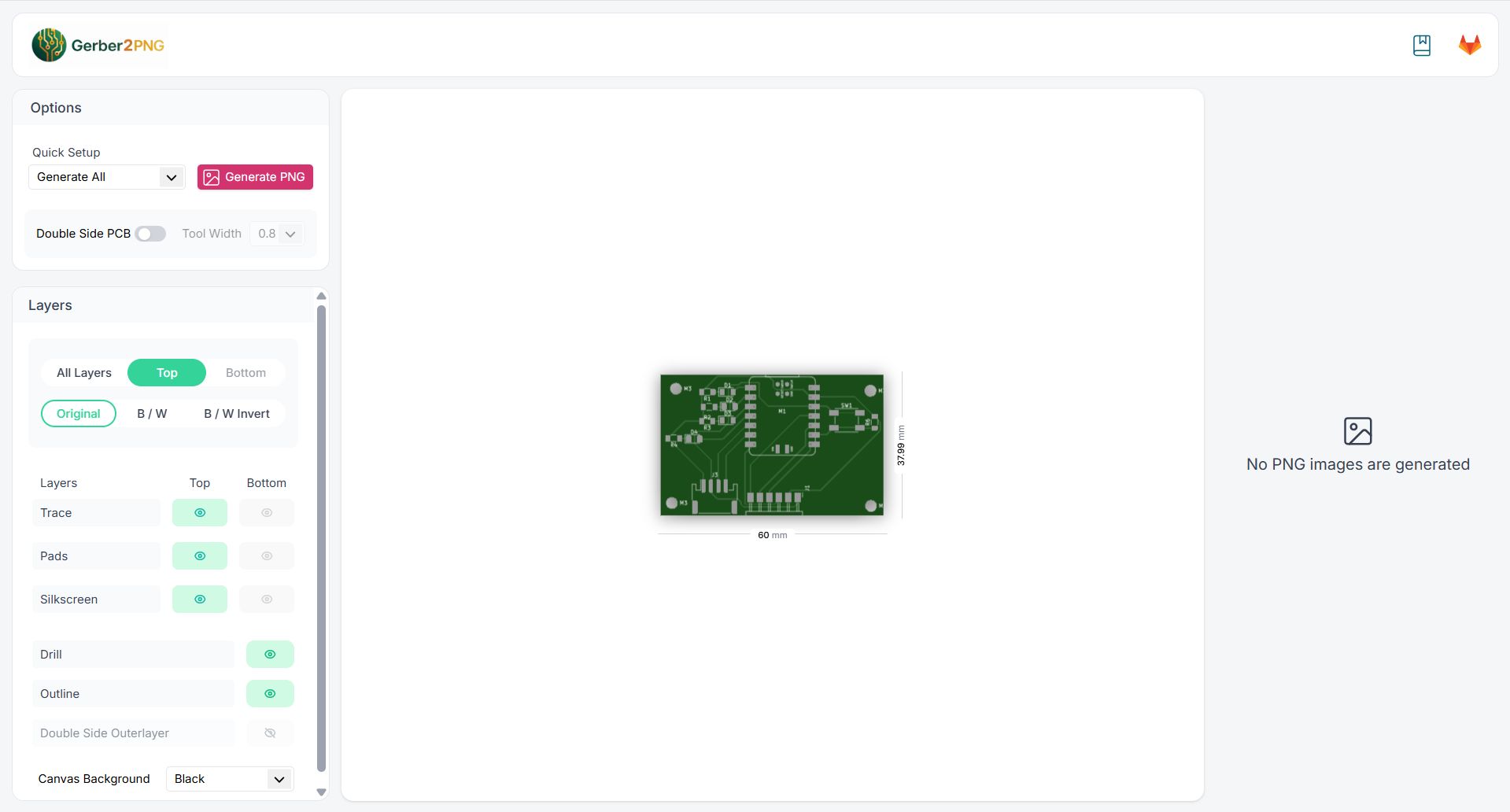
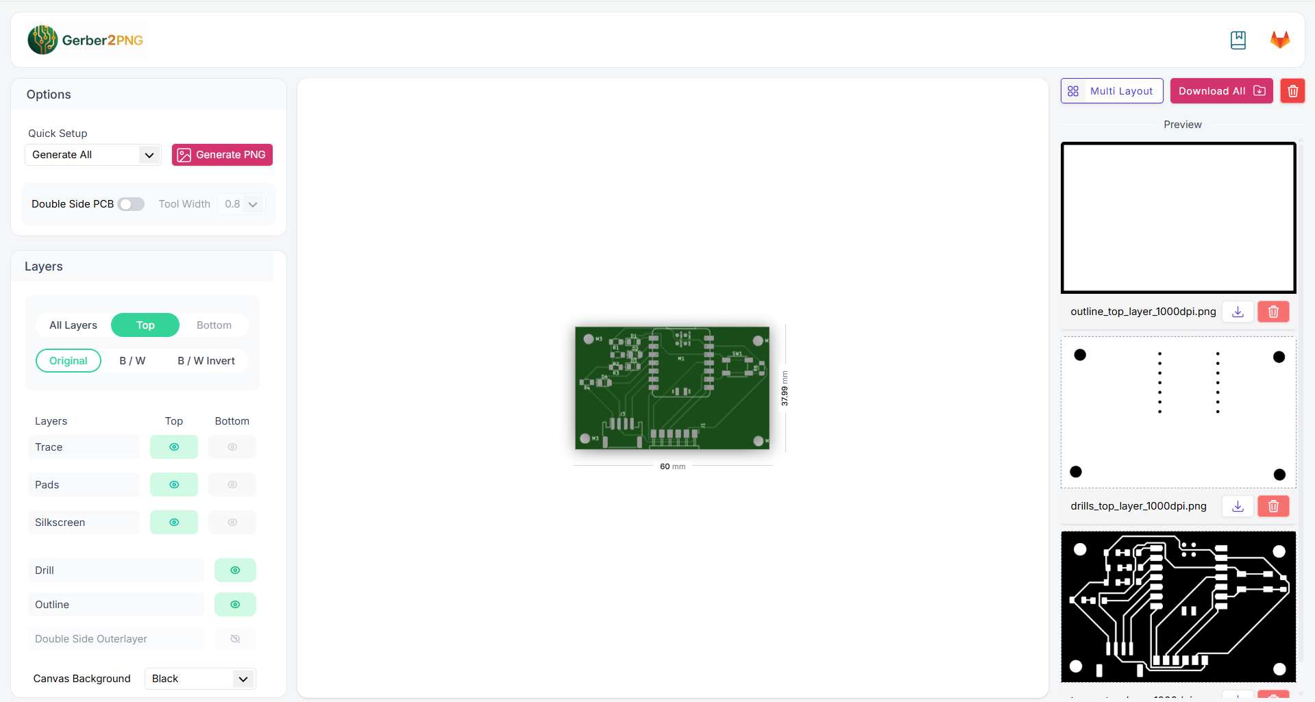
Exporting Gerber to PNG
Before using Fab Mods, I exported the PCB layers from KiCad as Gerber files, then converted them to high-resolution PNG images, the format required by Fab Mods to generate milling toolpaths.
Step 1: Open Fabrication Outputs
In the PCB Editor, go to File → Fabrication Outputs → Gerbers (.gbr)
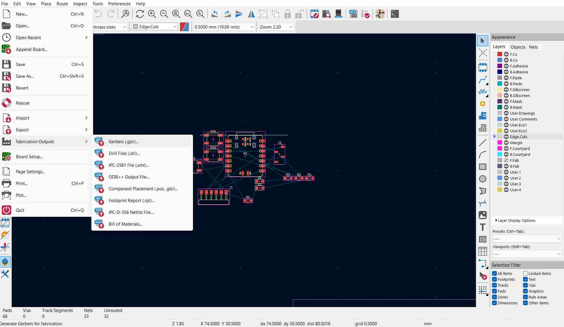
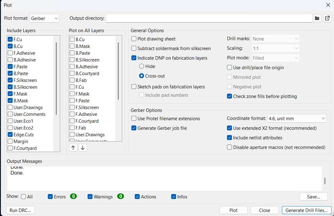
Step 2: Configure the Plot (Gerber) settings
The Plot dialog opens. Check the following settings before clicking Plot:
- Plot format — make sure it is set to Gerber.
- Output directory — choose a folder where the files will be saved.
- Include Layers — tick the layers you need. At minimum:
- F.Cu — front copper (your traces)
- B.Cu — back copper (if double-sided)
- F.Mask / B.Mask — solder mask openings
- F.Silkscreen / B.Silkscreen — component labels
- Edge.Cuts — board outline (required)
- Coordinate format — leave at 4.6, unit mm.
- Keep Use extended X2 format and Generate Gerber job file ticked.
Click Plot. The Output Messages box at the bottom will show Done. for each layer when it finishes.
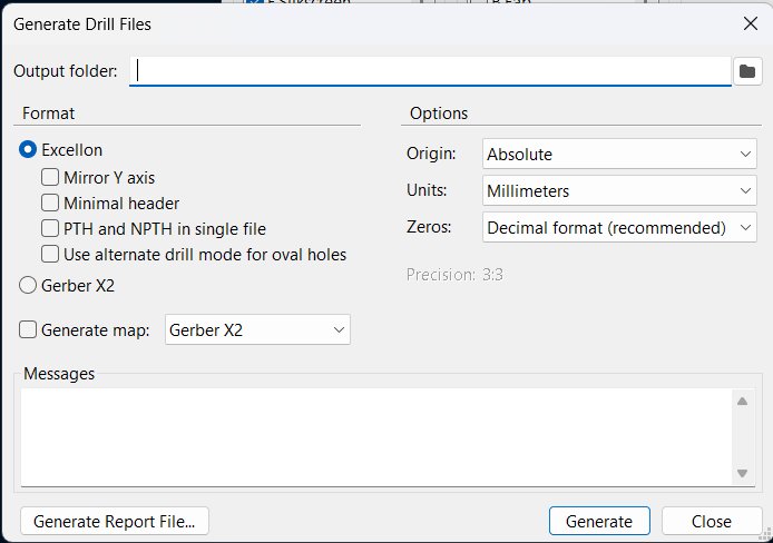
Step 3: Generate Drill Files
After plotting the Gerbers, click Generate Drill Files... at the bottom right of the Plot dialog. A new window opens.
- Output folder — use the same folder as your Gerber files.
- Format — leave as Excellon (the standard for most fabs and milling machines).
- Units — set to Millimeters.
- Zeros — leave as Decimal format (recommended).
- Origin — leave as Absolute.
Click Generate. Two drill files are created: PTH.drl (plated through-holes) and NPTH.drl (non-plated holes).
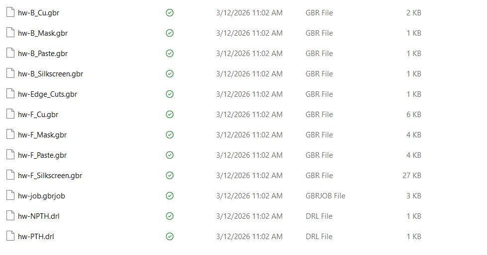
Step 4: Check the output files
Open the output folder. You should see a set of .gbr files (one per layer) and two .drl drill files:
- hw-F_Cu.gbr — front copper layer (traces)
- hw-B_Cu.gbr — back copper layer
- hw-F_Mask.gbr / hw-B_Mask.gbr — solder mask layers
- hw-F_Paste.gbr / hw-B_Paste.gbr — solder paste layers
- hw-F_Silkscreen.gbr / hw-B_Silkscreen.gbr — silkscreen labels
- hw-Edge_Cuts.gbr — board outline
- hw-job.gbrjob — job file that groups all Gerbers together
- hw-PTH.drl — plated drill holes
- hw-NPTH.drl — non-plated drill holes
Zip all these files together and send them to your PCB manufacturer, or load them into a Gerber viewer (like KiCad's built-in viewer or Fab Mods) to verify before fabrication.
Design Files
RP2040 Design Fileshere.
Attiny Design Fileshere.