INPUT DEVICES
Group Assignment
- Probe an input device's analog levels and digital signals
Individual Assignment
- Measure something: add a sensor to a microcontroller board that you have designed and read it
You can the click here to access the Group Assignment.
Input Devices
Input devices are the sensors and transducers that allow a microcontroller to perceive the physical world. They convert real-world phenomena — light, temperature, pressure, motion, touch, magnetic fields, sound — into electrical signals that a microcontroller can read, process, and act on.
Every embedded system starts with inputs. Without them, a microcontroller is blind to its environment. It can only execute fixed instructions with no awareness of what is happening around it. Input devices close that loop, enabling systems to sense, respond, and adapt in real time.
Input signals broadly fall into two categories:
- Analog inputs — continuously varying voltages (e.g. a temperature sensor outputting 0–3.3 V proportional to temperature). Read via an ADC (Analog-to-Digital Converter).
- Digital inputs — discrete high/low signals (e.g. a button press, a pulse from an encoder, or serial data from a digital sensor over I2C/SPI/UART).
This week's work focused on adding real sensor inputs to a custom-designed PCB — exploring how to select, wire, and read different types of sensors from a microcontroller.
Individual Assignment
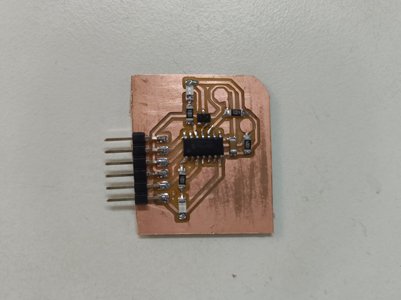
For this week I designed and milled a custom input board built around the ATtiny1624.
The board integrates two capacitive touch pads and a linear Hall effect sensor. These are all inputs that will eventually feed into my final project, a pill dispenser.
Below is the finished board after milling, soldering, and testing.
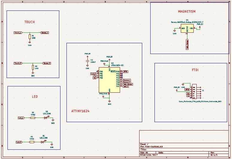
Schematic
The schematic was drawn in KiCad's schematic editor and is organised into four labelled blocks for clarity. Net labels (rather than direct wires) connect the blocks to the ATtiny1624 in the centre, keeping the sheet readable.
- TOUCH (top-left) — Touch_1 and Touch_2 nets, each with a 1 MΩ pulldown resistor (R1, R2) to GND, feeding into the ATtiny's GPIO pins PA4 and PA5.
- ATTINY1624 (centre) — all 14 pins labelled with their assigned nets: PA4/PA5 for touch, PA6 for Hall_Sense, PA7/PB3 for LED outputs, and PA0 for UPDI programming.
- MAGNETISM (top-right) — U1, the A1324 linear Hall effect sensor, with VDD tied to PWR_5V, GND, and the analog output routed to the Hall_Sense net on the ATtiny.
- LED (bottom-left) — D1 and D2 (green LEDs) with 470 Ω current-limiting resistors R3 and R4, driven from the LED_1 and LED_2 GPIO nets.
- FTDI (bottom-right) — J1, a 6-pin flat header (CUI footprint) providing the UPDI programming connection, protected by R5 (470 Ω inline resistor).
Project Context
Board Overview
| Microcontroller | ATtiny1624 (14-pin SOIC, tinyAVR 2-series) |
| Operating voltage | 5V |
| Inputs | 2 capacitive touch pads, 1 Hall effect sensor (A1324) |
| Outputs | 2 green LEDs (visual feedback for touch) |
| Programming | UPDI via SerialUPDI with FTDI adapter |
How Capacitive Touch Sensing Works
The touch pad is a 12 mm exposed copper circle on the PCB. A 1 MΩ resistor connects from the pad to GND as a pulldown.
The ATtiny charges the pad high through the GPIO pin, then switches to input mode and measures how long it takes for the charge to drain through the 1 MΩ resistor. When a finger touches the pad, it adds capacitance (~10–30 pF), which slows the discharge. The ATtiny detects this timing difference to determine if the pad is being touched.
- The 1 MΩ resistor is a pulldown to GND, not inline between GPIO and pad
- The GPIO pin connects directly to the copper pad
- No external sensor IC needed — sensing done in software via GPIO charge/discharge timing
- Works on any digital GPIO pin on the ATtiny
How the Hall Effect Sensor Works
The A1324 is a linear Hall effect sensor that outputs an analog voltage proportional to the magnetic field strength. With no magnet nearby, the output sits at approximately half the supply voltage (~2.5 V at 5 V supply). A south pole magnet increases the output toward VCC, while a north pole decreases it toward GND.
In the pill dispenser, a magnet embedded in each rotor disc passes over the sensor to detect disc position.
- A1324 requires 4.5 V–5.5 V supply — does NOT work at 3.3 V
- Output connects directly to ATtiny ADC pin — no pullup resistor needed
- The A1324 has an active push-pull output stage (unlike open-collector Hall switches like the A3144)
- A 100 nF bypass capacitor is placed close to the sensor for clean power
Design Rules
- Minimum trace width: 0.4 mm
- Minimum clearance: 0.4 mm
- All SMD components: 1206 package size
- Single-layer PCB, milled on Roland SRM-20
- 1/64" endmill for traces, 1/32" endmill for board outline
PCB Design
The PCB was designed in KiCad's PCB Editor as a single-layer board to be milled on the Roland SRM-20. All components are SMD 1206 footprints placed on the front copper layer (F.Cu), routed with a minimum trace width of 0.4 mm.
Board Layout
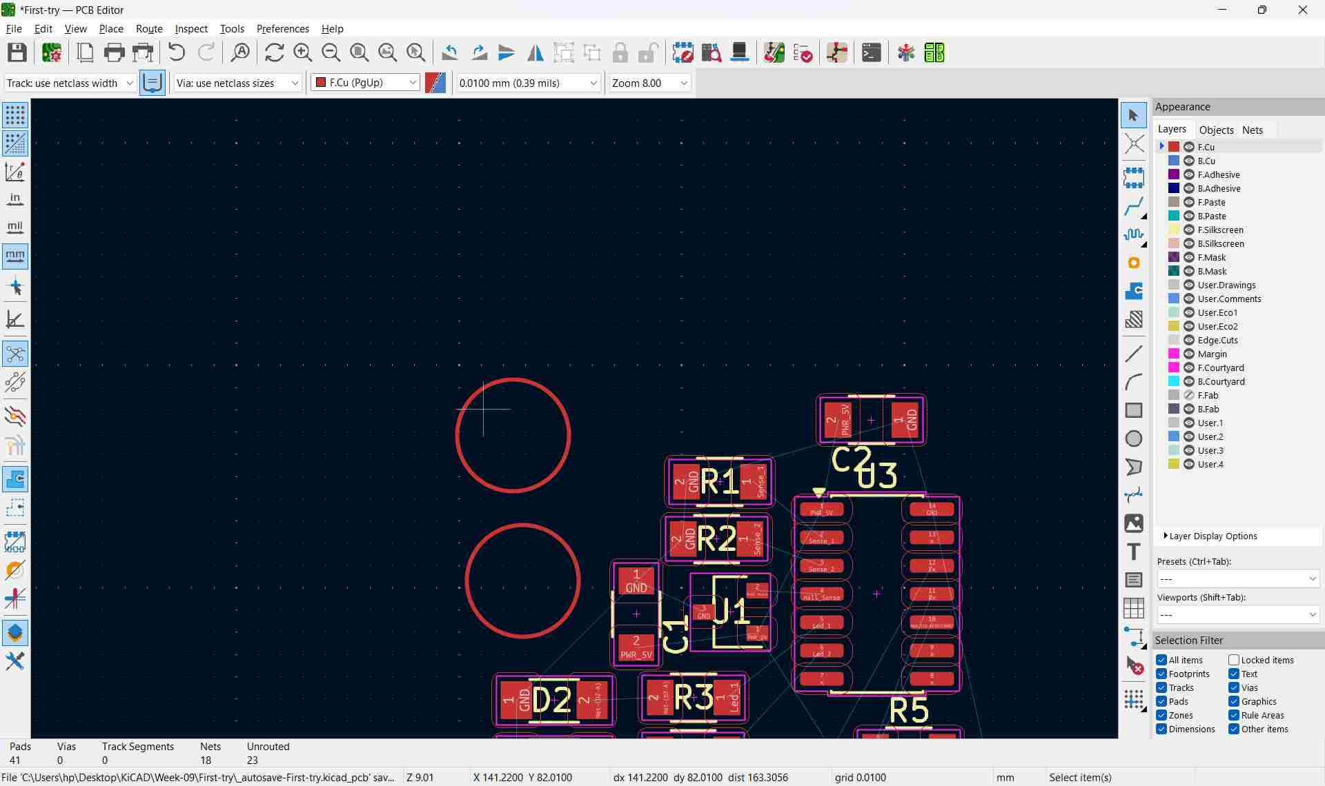
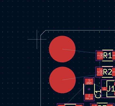
On the image above, on the left are two large circles,these are the capacitive touch sense pads that users will physically press. They are drawn directly on F.Cu as filled copper circles assigned to the sense net, rather than as standard pad footprints.
Creating the Capacitive Touch Pads
Because KiCad doesn't have a built-in "touch pad" footprint, the sense pads were drawn manually using the Circle tool on the F.Cu layer. After placing the circle outline, properties had to be set to make it electrically functional.
Right-clicking the circle opens the context menu, where Properties (E) gives access to geometry and net assignment:
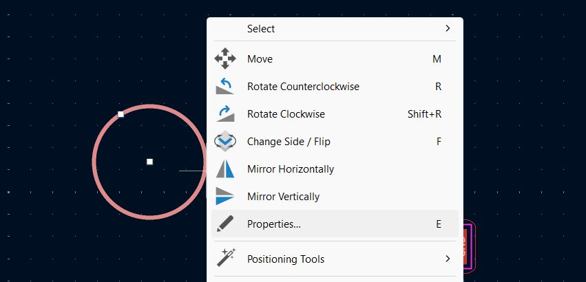
This is the properties panel that opens up
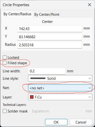
Initially the circle is just a graphic, it has no net (<no net>) and Filled shape is unchecked. In this state it is a courtyard or silkscreen-style outline and carries no electrical signal.
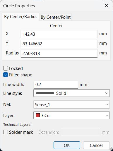
To turn the circle into a real copper pad, two changes were made in the Properties dialog:
- Filled shape was checked — this floods the circle area with solid copper, giving a continuous conductive surface for the finger to touch.
- Net was set to
Sense_1— this connects the copper pad to the same net as the ATtiny ADC pin and the 1 MΩ pulldown resistor, so KiCad's DRC can verify connectivity and the pad participates in routing.
Touch Pad Close-up
With both circles filled and assigned to their respective nets, the two capacitive touch pads appear as large solid copper discs on the left side of the board.
The traces leading from each pad route toward R1 and R2 (the 1 MΩ pulldown resistors) and onward to the ATtiny1624 GPIO pins.
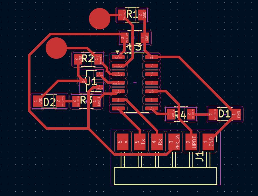
Complete Board Layout
The full board layout shows all components placed and routed on a single copper layer (F.Cu).
The two touch pads sit at the top-left. The ATtiny1624 (SOIC-14) occupies the centre.
R2 and U1 (the A1324 Hall effect sensor in its TO-92 footprint) are on the left branch,while R4 and D1 are on the right branch.
D2 and R3 sit at the far left for touch pad 2 feedback.
J1 (the UPDI programming header) runs along the bottom edge.
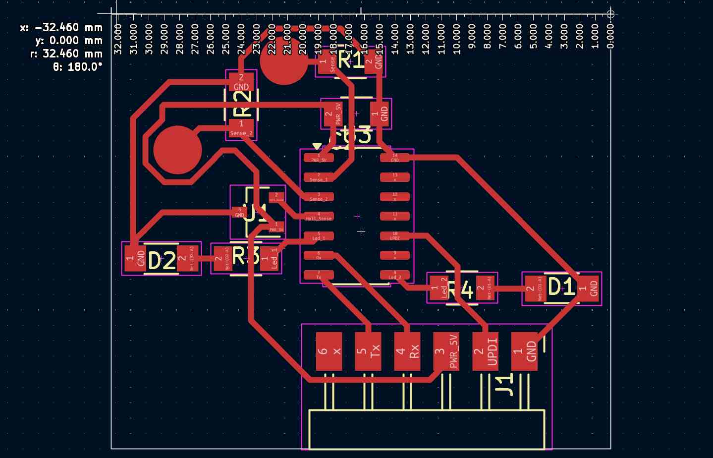
Board Dimensions
Using KiCad's measurement tool, the board width was verified. The coordinate readout (x: −32.460 mm, r: 32.460 mm, θ: 180°) confirms the board spans approximately 32.5 mm horizontally — sized to fit within the Roland SRM-20's usable milling area while keeping all components accessible.
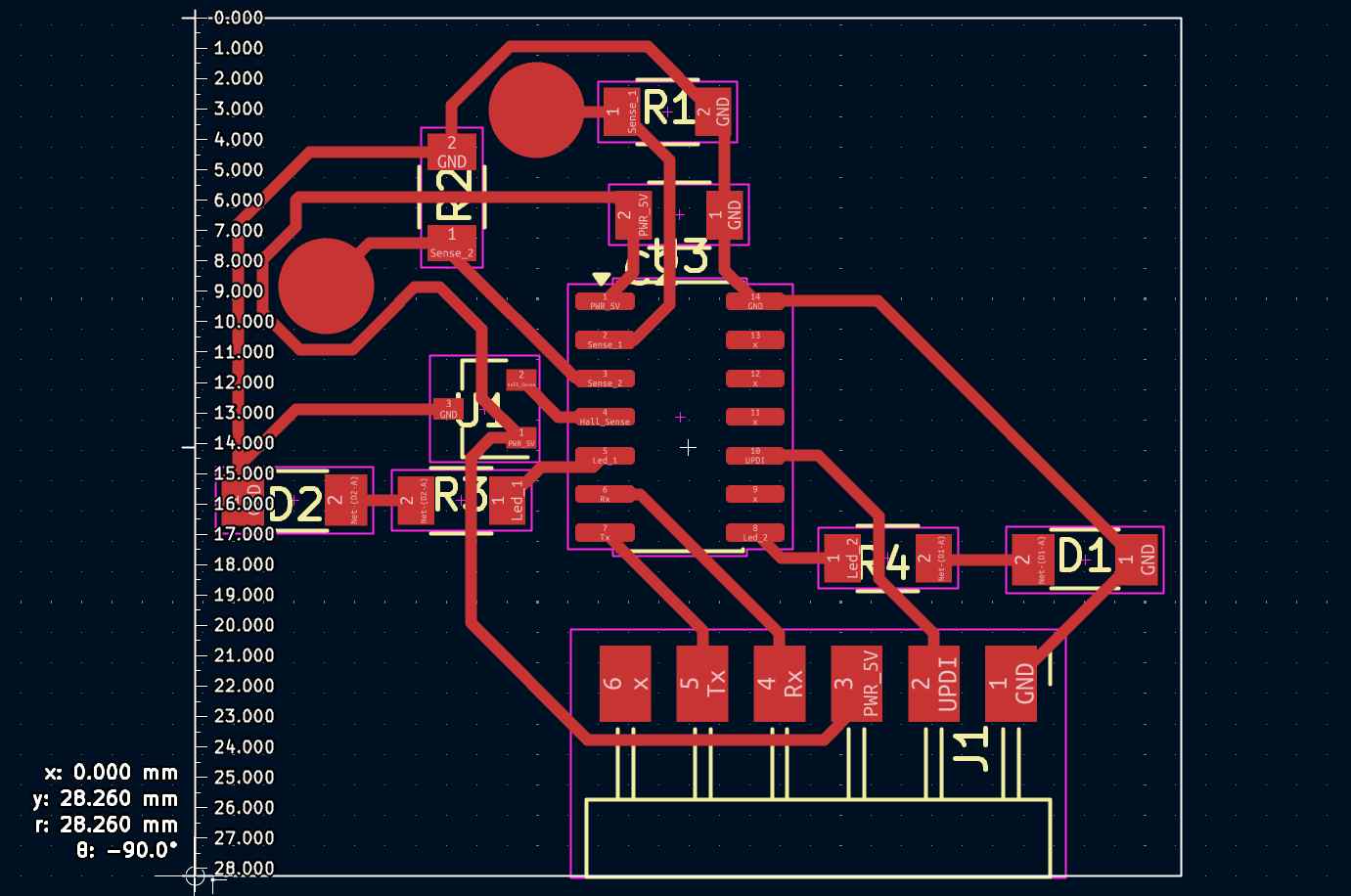
The vertical dimension was measured similarly. The readout (y: 28.260 mm, r: 28.260 mm, θ: −90°) gives a board height of approximately 28.3 mm. The ruler guides along the left and bottom edges confirm the overall footprint of the board before sending it to the milling machine.
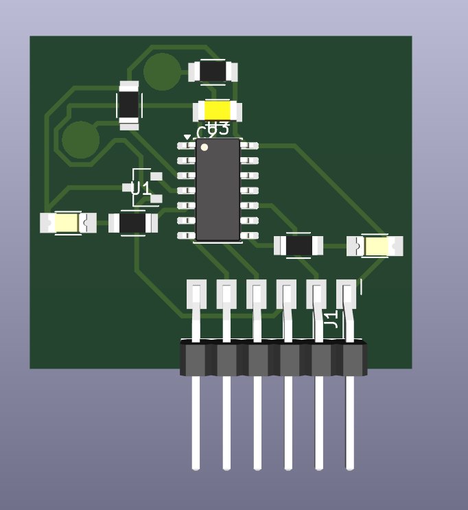
3D Render
KiCad's 3D viewer was used to verify component placement and check for mechanical clearance before sending the board to the milling machine. The render shows the ATtiny1624 (SOIC-14) at the centre, the two capacitive touch pads as raised dark-green copper circles on the top-left, and J1 (the UPDI programming header) as a through-hole connector protruding from the bottom edge. The yellow-highlighted component near the top is C3, the 100 nF decoupling capacitor placed close to the ATtiny's VDD pin. All SMD components are 1206 footprints, visible as grey rectangular bodies with silver pads.
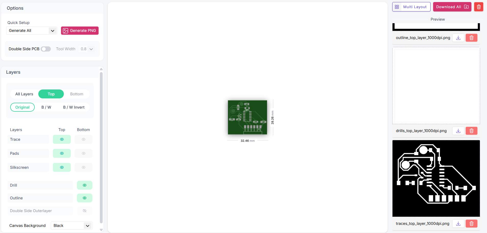
Exporting Milling Files with Gerber2PNG
Before milling, the KiCad Gerber files were converted to PNG images using Gerber2PNG — an online tool that renders each board layer as a separate high-resolution image. The tool shows the board preview at the correct dimensions (32.46 × 28.26 mm) and generates one PNG per layer. The layer visibility panel on the left shows the Top layers (Trace, Pads, Silkscreen) enabled and the Bottom layers hidden, since this is a single-sided board. Three files were generated and are visible in the preview panel on the right:
- outline_top_layer_1000dpi.png — the board boundary/outline used to cut the PCB to shape
- drills_top_layer_1000dpi.png — drill positions for through-hole components (J1 header pins)
- traces_top_layer_1000dpi.png — the copper trace layer (shown in white on black), used to drive the milling toolpaths on the Roland SRM-20
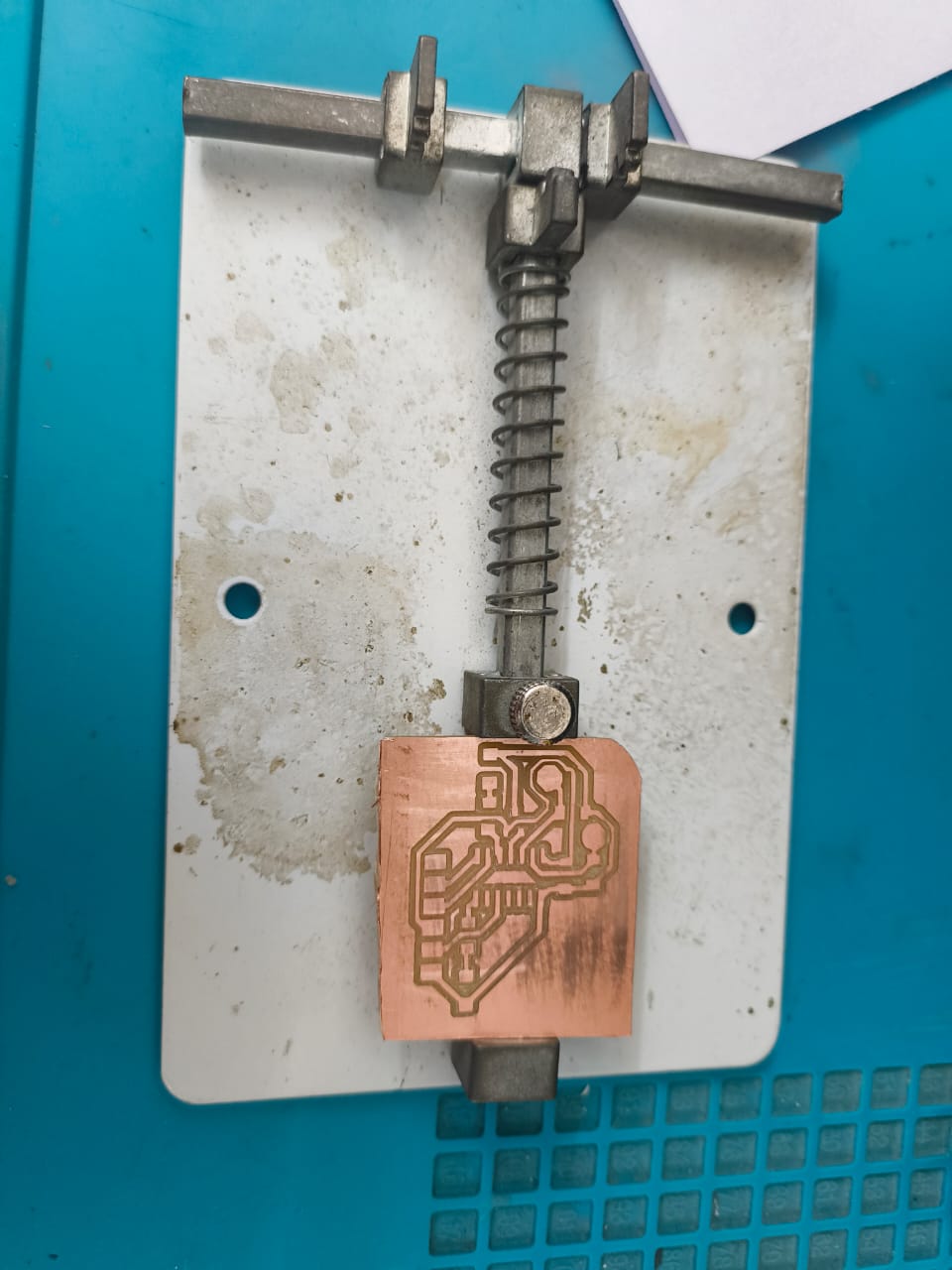
Milling, Assembly and First Power-Up
The board was then milled using the Roland machine. To know more about the milling process, refer to the previous week's documentation.
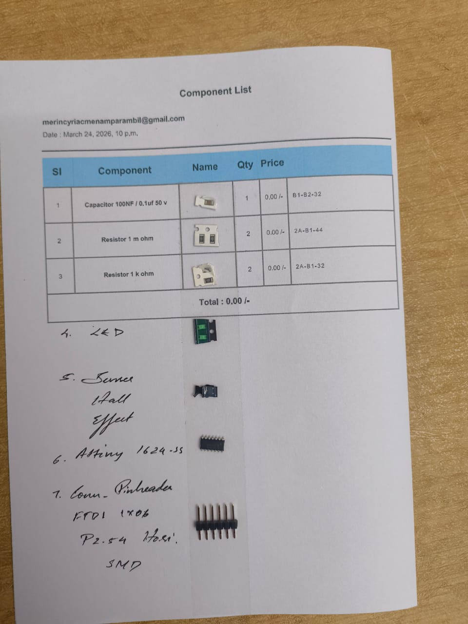
After milling, I requested each component I would need, from the Kochi Fablab's digital inventory. Then I printed the sheet out and placed the components in their respective sots.
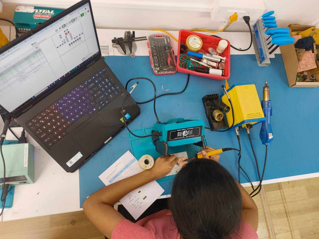
Then soldering began.
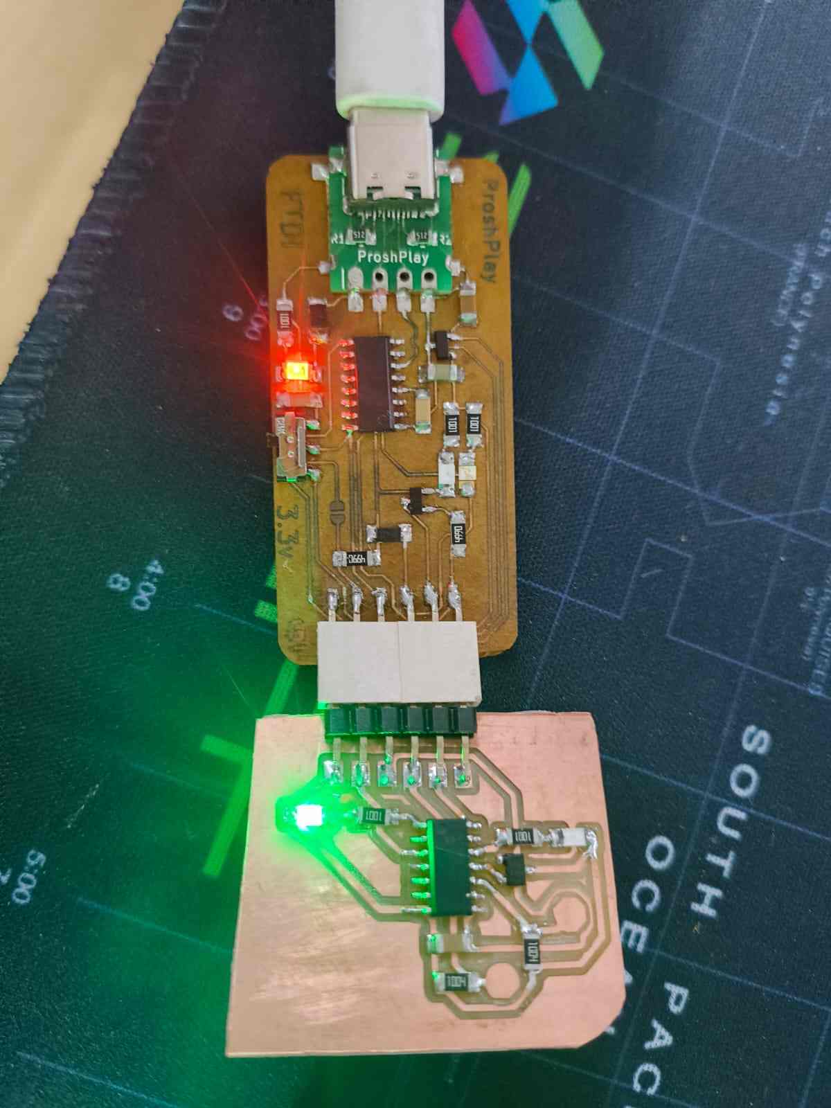
Fully soldered board.
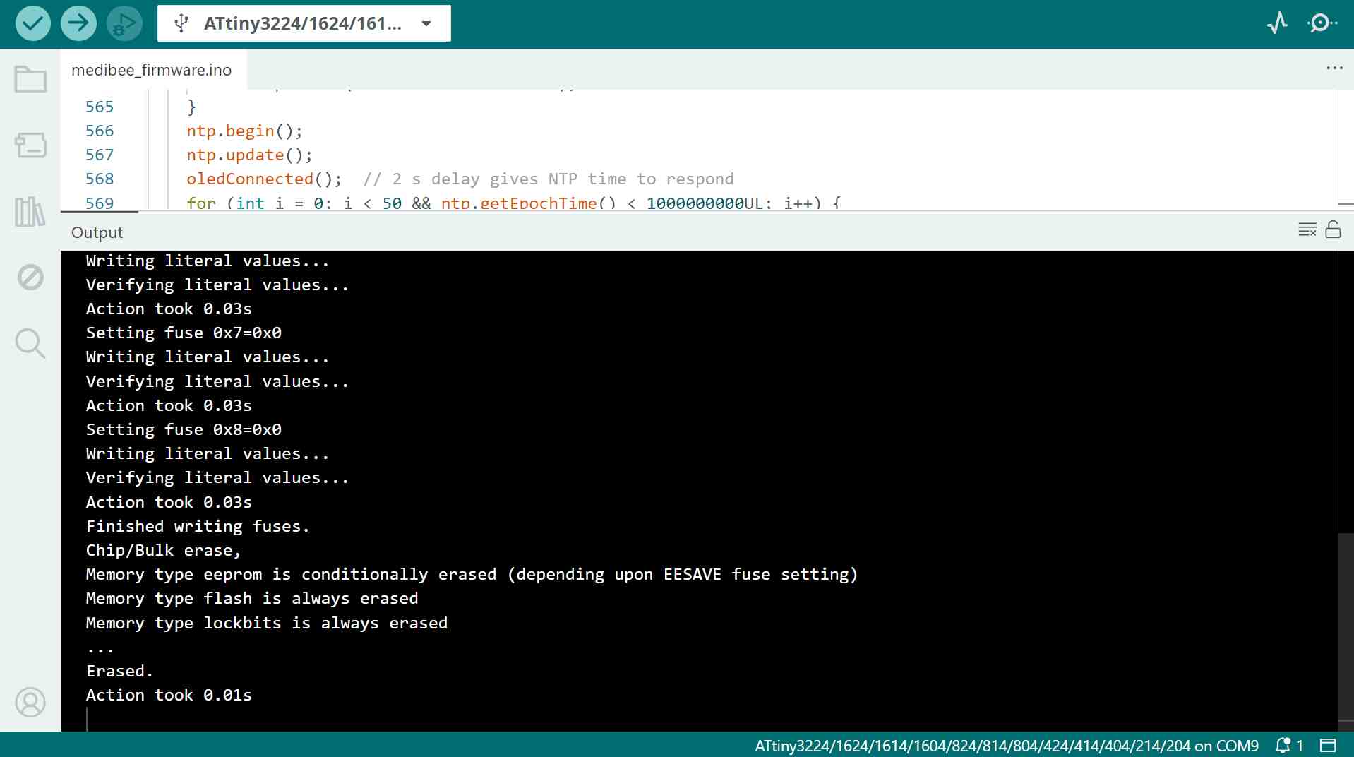
Once fully assembled, the board was connected to a ProshPlay UPDI programmer via the 6-pin FTDI header to verify power and prepare for firmware upload.
Programming the ATtiny1624
The ATtiny1624 uses UPDI for programming and is not supported in Arduino IDE by default. Here's the full setup from scratch.
Step 1 — Install Arduino IDE
Download and install Arduino IDE 2.x from arduino.cc/en/software if you don't have it already.
Step 2 — Install megaTinyCore
megaTinyCore is the board package by Spence Konde that adds support for the ATtiny1624.
- Open Arduino IDE and go to File > Preferences
- In "Additional Board Manager URLs", paste:
http://drazzy.com/package_drazzy.com_index.json
- Click OK
- Go to Tools > Board > Boards Manager
- Search for megaTinyCore by Spence Konde and click Install
Step 3 — Configure Board Settings
Go to Tools and set each option as follows:
| Setting | Value |
|---|---|
| Board | Tools → Board → megaTinyCore → ATtiny1624 |
| Chip | ATtiny1624 |
| Clock | 20 MHz internal (no crystal needed) |
| millis()/micros() Timer | TCA0 (default) |
| Programmer | SerialUPDI - SLOW: 57600 baud (more reliable to start with) |
| Port | The COM port of your FTDI adapter (e.g., COM3, COM5) |
Program Code
The firmware was written in Arduino (C++) using the megaTinyCore library. It reads both capacitive touch pads using an RC discharge timing method and reads the A1324 Hall effect sensor via the ADC. LED feedback is given for each touch input, and all sensor values are streamed over Serial at 115200 baud for debugging.
Prompt
This is the prompt I used to generate the code with AI:
Sketch
// ATtiny1624 Input Board — touch x2, Hall sensor, LED feedback
// megaTinyCore | 20MHz internal | SerialUPDI

#define TOUCH_1   PIN_PA4
#define TOUCH_2   PIN_PA5
#define HALL      PIN_PA6
#define LED_1     PIN_PA7
#define LED_2     PIN_PB1

const uint16_t TOUCH_THRESHOLD = 100;   // tune after baseline read
const uint16_t HALL_DELTA      = 80;    // ADC counts from idle to trigger

uint16_t hallIdle = 0;

// RC discharge timing: charge pad HIGH, time drain through 1M pulldown
uint16_t readTouch(uint8_t pin) {
  pinMode(pin, OUTPUT);
  digitalWrite(pin, HIGH);     // charge pad
  delayMicroseconds(50);
  pinMode(pin, INPUT);         // release, let it drain
  uint16_t t = 0;
  while (digitalRead(pin) == HIGH && t < 5000) t++;  // count drain time
  return t;                    // finger adds C -> slower drain -> higher t
}

void setup() {
  Serial.begin(115200);
  pinMode(LED_1, OUTPUT);
  pinMode(LED_2, OUTPUT);
  analogReference(VDD);
  hallIdle = analogRead(HALL); // baseline ~512 (2.5V at 5V)
  Serial.print("Hall idle: ");
  Serial.println(hallIdle);
}

void loop() {
  uint16_t t1 = readTouch(TOUCH_1);
  uint16_t t2 = readTouch(TOUCH_2);
  uint16_t hall = analogRead(HALL);
  int hallDiff = (int)hall - (int)hallIdle;

  bool touched1 = t1 > TOUCH_THRESHOLD;
  bool touched2 = t2 > TOUCH_THRESHOLD;
  bool magnet   = abs(hallDiff) > HALL_DELTA;

  digitalWrite(LED_1, touched1);
  digitalWrite(LED_2, touched2);

  Serial.print("T1:"); Serial.print(t1);
  Serial.print(" T2:"); Serial.print(t2);
  Serial.print(" Hall:"); Serial.print(hall);
  Serial.print(" Mag:"); Serial.println(magnet ? "YES" : "no");

  delay(100);
}- Touch sensing —
readTouch()charges the pad HIGH via GPIO, then releases it to drain through the 1 MΩ pulldown. It counts loop iterations until the pin reads LOW. A finger adds capacitance, slowing the drain — a higher count means a touch is detected. - Hall sensor —
analogRead(HALL)reads the A1324 output voltage. At startup,hallIdlecaptures the baseline (~512 counts at 5 V). During the loop, the difference from idle is compared againstHALL_DELTAto detect a magnet. - LED feedback — LED_1 lights when Touch_1 is active; LED_2 lights when Touch_2 is active.
- Serial output — All four values (T1, T2, Hall ADC count, Magnet detected) are printed every 100 ms for live monitoring in the Arduino Serial Monitor.