Week 8 - Electronic Product Manufacturing
This week we start learning Electronics Production . If the previous electronic design mainly focused on schematics and PCB files, then this week's focus is to actually turn the design into a working circuit board. This process includes PCB fabrication, board surface cleaning, soldering and assembly, short-circuit detection, firmware programming, and functional verification.
Electronic product manufacturing is a crucial link in the digital manufacturing project's transition from "design documents" to "physical hardware". Even if a circuit board passes inspection in software, it may still fail to function properly during actual production due to issues such as tool parameters, board fixation, soldering quality, or copper shavings short-circuiting. Therefore, this week's learning focus is to understand the PCB manufacturing process and master basic processing and debugging methods through hands-on practice.
Group assignment:
The group assignment mainly involves formulating PCB manufacturing specifications suitable for laboratory working conditions. The content includes tool selection, platform zeroing, milling parameters, safety requirements, and document preparation, etc. At the same time, it is necessary to understand how to submit the designed circuit board files to PCB manufacturers for production, including exporting Gerber files and drilling files, etc.
Individual assignment:
The individual assignment is to independently fabricate a development board and complete PCB milling, soldering, programming, and testing. During the fabrication process, it is necessary to clarify hardware selection, key interfaces, and circuit design concepts, and frequently use a multimeter for detection during processing and soldering to avoid short circuits or cold solder joints. Finally, verify whether the functions of the development board are normal by programming the program.
Overall, the focus of this week was not on designing complex circuits, but on experiencing the entire manufacturing process of a PCB from design files to a physical board. Through this exercise, I have gained a more concrete understanding of the relationships among PCB processing parameters, pre-soldering inspection, post-soldering debugging, and program verification.
Group Assignment
Group Assignment Page: https://fabacademy.org/2026/labs/chaihuo/docs/week8/week8_group_assignment
1. Design rules for PCB production process
This group assignment mainly focuses on the process of making PCBs using a desktop CNC in the laboratory. Compared to factory PCB manufacturing, the advantages of making PCBs in the laboratory are fast speed and suitability for rapid verification; however, it is also more dependent on tool condition, platform flatness, board fixation, and parameter settings. Therefore, before formal processing, it is necessary to first develop a set of manufacturing specifications suitable for laboratory working conditions.
1.1 Tool Selection
PCB milling typically uses V-shaped engraving cutters or small-diameter milling cutters. V-shaped cutters are suitable for copper foil isolation engraving, where the actual cutting width can be controlled by the depth of cut; small-diameter milling cutters are more suitable for contour cutting or cleaning wider areas.
This PCB manufacturing mainly uses V-shaped engraving cutter for circuit isolation. The reason for choosing the V-shaped cutter is that its tip is relatively thin, which can process narrower isolation grooves and is suitable for the production of small circuits on single-sided copper-clad boards.
| Tool Type | Main Uses | Precautions |
|---|---|---|
| V-shaped carving knife | Line isolation, carving around pads | Excessive cutting depth will result in an overly wide isolation groove |
| Flat end mill | Edge cutting, area copper cleaning | The large diameter is not suitable for densely packed circuits |
| Drill Bit | Drilling | This design tries to avoid drilling as much as possible |
Due to the limited stability and precision of CNC, the line spacing cannot be set too extreme when designing PCBs. Compared with factory board manufacturing, laboratory milling requires more space to be reserved for tool errors and board warping.
1.2 Platform Calibration and Zeroing
Platform calibration is a very crucial step in PCB processing. The surface of the copper-clad laminate must be as flat as possible; otherwise, the same cutting depth will produce different effects at different positions: in some areas, the copper foil cannot be cut through, while in others, the cutting will be too deep.
The basic zeroing procedure is as follows:
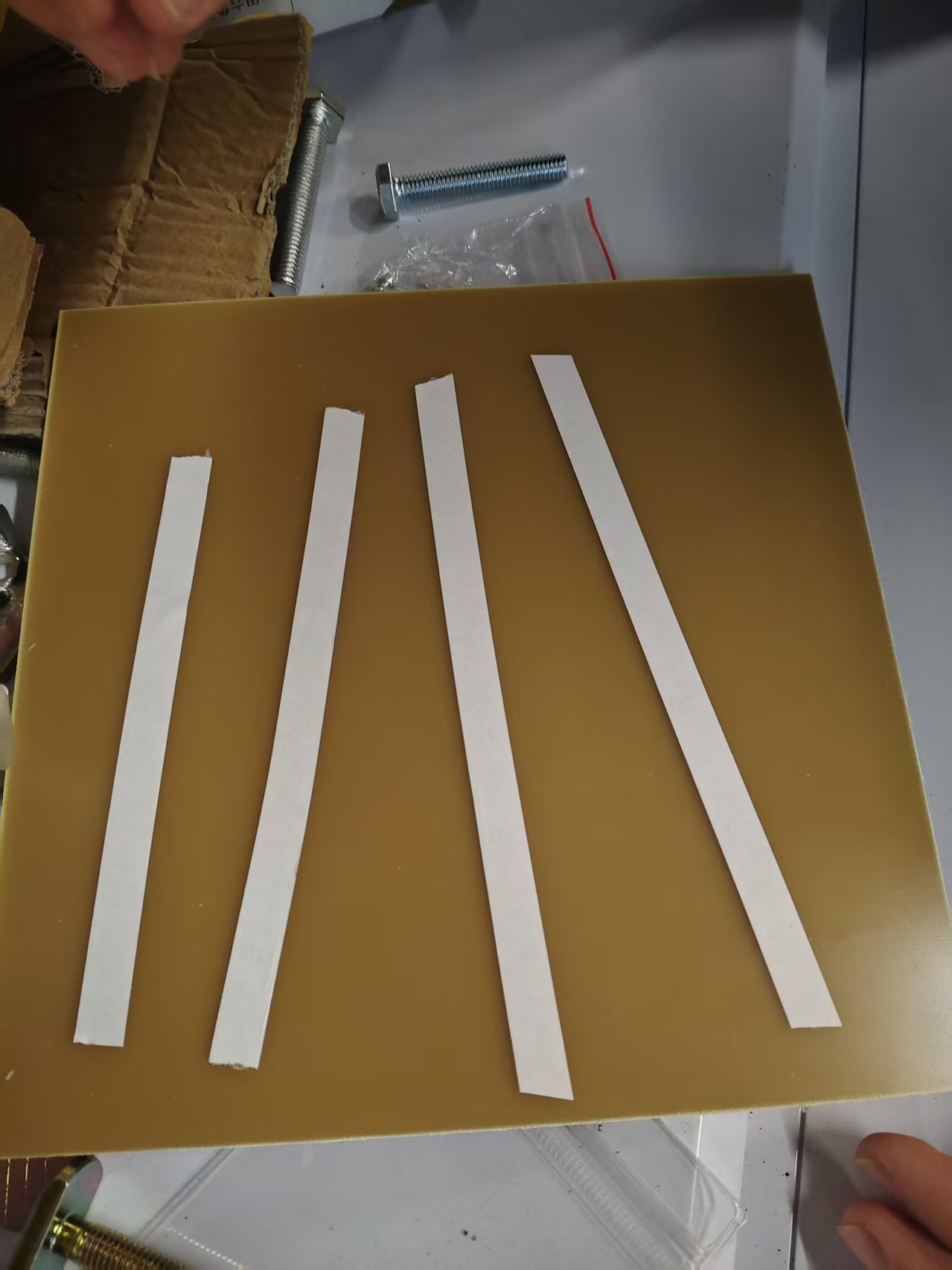
- Secure the copper-clad laminate flat on the CNC workbench.
- Check if the panel is warped, and use double-sided tape or a pressing plate to assist in fixing if necessary.
- Move the tool near the machining starting point.
- Slowly lower the Z-axis until the tool tip just touches the copper surface.
- Set the current coordinate as the zero point of the Z-axis.
- Perform a dry run or local trial engraving to confirm that the tool path and depth are correct.
Special care must be taken during zero adjustment to prevent the tool tip from quickly hitting the plate surface. The tool tip is very thin, and once it collides with the tool or presses down too much, it is very easy to break.
1.3 Recommended Processing Parameters
Based on the current laboratory conditions, we have compiled the basic parameters suitable for single-sided copper-clad laminate engraving. During actual processing, fine adjustments still need to be made according to tool wear, board flatness, and circuit density.
| Project | Recommended Parameters | Description |
|---|---|---|
| Tool | V-shaped carving knife | for line isolation |
| Cutting Depth | 0.1 mm | Try to etch through only the copper foil and avoid damaging the substrate too deeply |
| Feed Rate | 15 mm/s | Excessive speed can easily lead to tool breakage or burr formation |
| Sheet Material | Single-sided copper-clad laminate | Suitable for rapid prototyping in the laboratory |
| Processing Method | Single-sided carving | Reduce the difficulty of alignment and drilling |
| Line Design | Line width ≥ 0.4 mm | Leave margin for CNC machining error |
| Line Spacing / Isolation Gap | ≥ 0.3 mm | Reduce the risk of short circuit |
The cutting depth is an important parameter that affects the quality of the finished product. If the depth is too shallow, the copper foil will not be completely disconnected, resulting in a short circuit; if the depth is too deep, the isolation groove will widen, and may even cause the copper foil to lift or the tool to be damaged.
2. PCB Design Rules
The PCB design used by this group was completed based on JLCPCB EDA , with the design goal of adapting to desktop CNC engraving of single-sided copper-clad boards while also retaining the possibility of subsequent submission to PCB manufacturers for board fabrication.
2.1 Schematic Design
The PCB design work for this project was completed based on JLCPCB EDA , covering the entire process from schematic drawing, library file creation, PCB layout and routing to production file export, and is suitable for both desktop CNC engraving and factory PCB manufacturing scenarios.
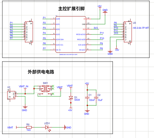
The schematic design is centered around the ESP32-C3 development board and mainly includes a power supply module, main control pin expansion, and external interfaces.
2.1.1 Power Supply Module
The circuit is connected to a 5V power supply through an external power socket with a 2.54 mm pitch, and a toggle switch is used to control the power on/off. An SS34 Schottky diode is added to the power input section to prevent reverse power connection; meanwhile, 10 uF and 100 nF capacitors are added for filtering to make the power supply more stable. The power indicator is connected to the power line through a 1k current-limiting resistor to indicate whether the board is powered on.
2.1.2 Main Control Pin Expansion
The common interfaces of ESP32-C3 are led out to the pin headers / sockets, including analog inputs, I2C, UART, SPI, and power pins. This allows for convenient connection of sensors, LED modules, or other peripherals in the future.
2.1.3 Overall Design Considerations
To adapt to desktop CNC production, the circuit should use single-sided boards, no vias, full SMT or top-layer soldering as much as possible. This can reduce the steps of drilling and double-sided alignment, thus lowering the difficulty of laboratory processing.
2.2 PCB Layout Design
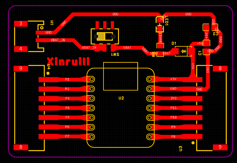
The layout of this PCB is mainly optimized for desktop CNC machining:
- Zero vias, all top-layer traces: Throughout the board, vias and through-hole components should be avoided as much as possible to reduce the drilling process.
- Relax line width and line spacing : The trace width should be controlled to be at least 0.4 mm, and the line spacing and isolation groove should be reserved with at least 0.3 mm.
- Rectangular pads: Longer pads are used at the main control and socket positions to increase the soldering contact area and reduce the impact of engraving deviation.
- Thickening of power supply traces : Thickening power supply lines such as +5V, VBAT, and GND reduces voltage drop and also minimizes the risk of thin traces being cut.
- Clear wiring partitioning: Power modules, main control modules, and expansion interfaces should be arranged in separate partitions as much as possible to reduce cross wiring.
- Rounded corner treatment for the plate frame : The shape uses a rectangle with rounded corners, which facilitates fixing and later use, and also reduces edge chipping.
These designs are not aimed at pursuing the minimum size, but rather at improving the success rate of laboratory processing. For desktop CNC, although extremely thin traces and densely packed pads are feasible in software, short circuits, open circuits, or copper foil lifting are likely to occur during actual processing.
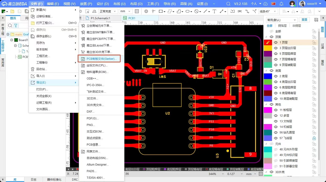
3. From Gerber to G-code
After completing PCB design in JLCPCB EDA, it is necessary to export PCB manufacturing files. Through the "File - Export" function of the software, standard Gerber files can be exported. Gerber files contain information such as circuit layers, pads, and outlines, and are the basis for PCB manufacturing and CNC conversion.

The exported Gerber files can be converted to G-code recognizable by CNC through online tools:
Conversion Tool: https://webgcode.vercel.app/
During conversion, parameters such as tool diameter, carving depth, and feed rate need to be set according to actual processing requirements. After conversion is completed, G-code files for line isolation carving and contour cutting can be obtained.
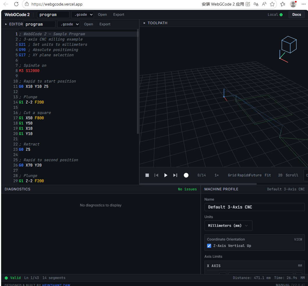
The G-code file generated this time:
暂时无法在飞书文档外展示此内容
4. CNC Cutting Process
4.1 Plate Fixing
Before processing, the copper-clad laminate must first be flatly fixed on the workbench to ensure that the board surface has no obvious warping or gaps. Loose fixing of the board will directly affect the engraving depth, resulting in some areas not being engraved through and some areas being cut too deeply.
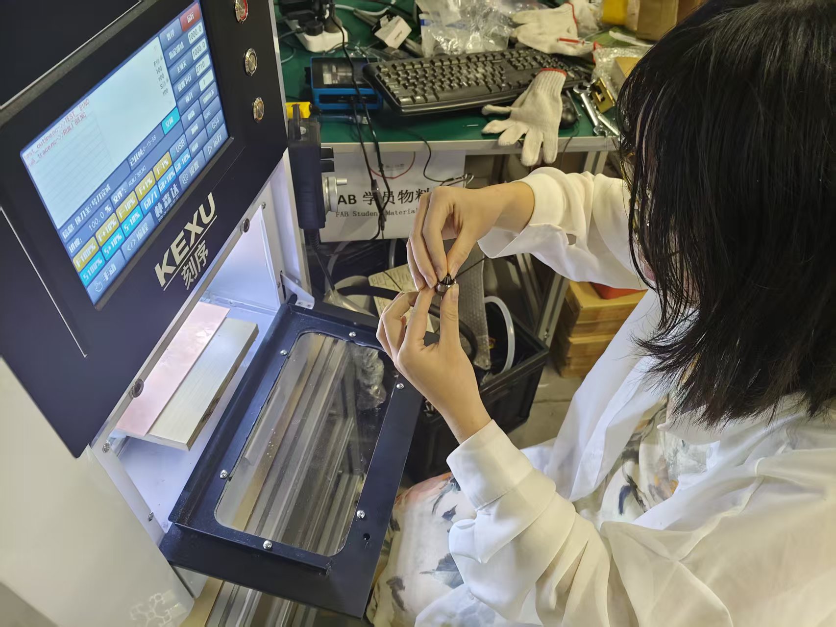
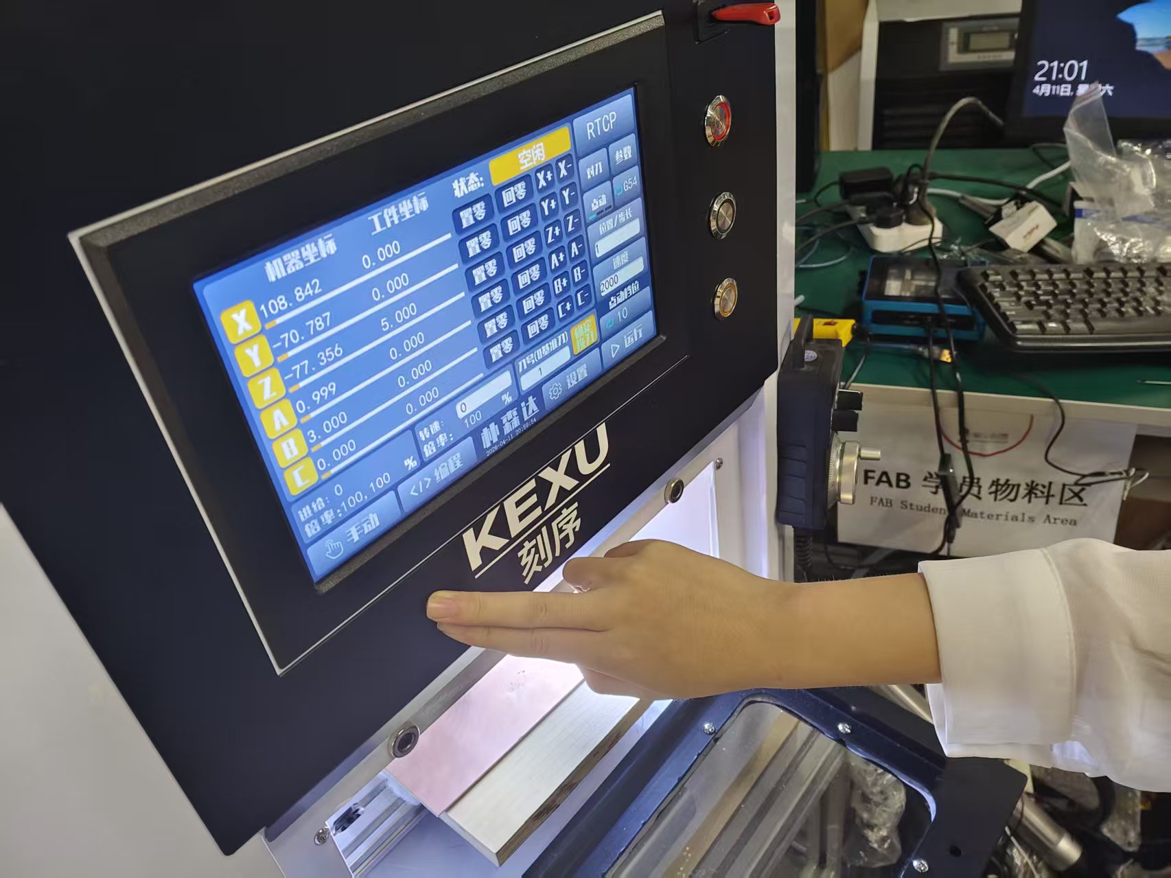
4.2 Tool Setting and Trial Run
After the plate is fixed, tool setting and zero adjustment are required. During tool setting, make the tool tip just touch the copper surface and set the current position as the Z-axis zero point. Before the formal machining, the idle running path can be run first to confirm that the tool path will not exceed the plate range and will not interfere with the fixture.
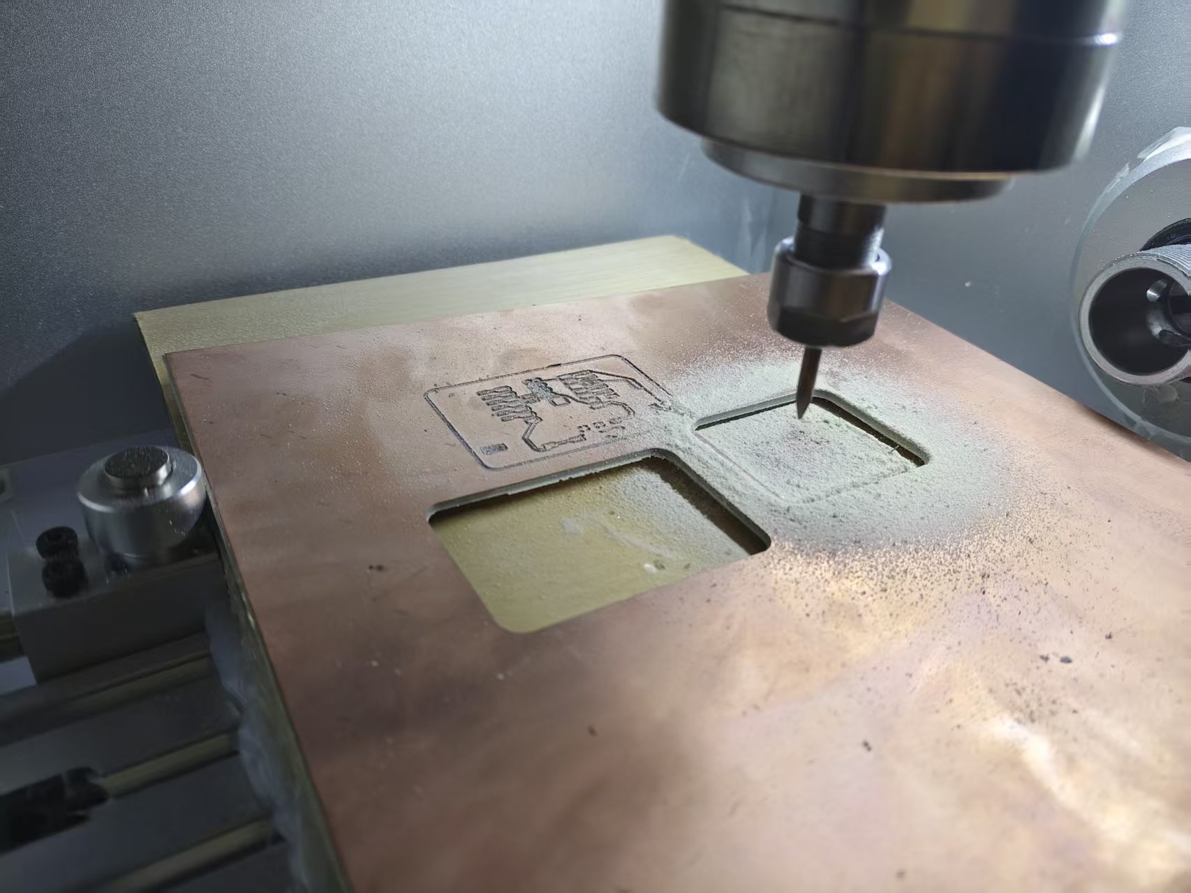
4.3 Carving and Post-processing
During formal processing, first complete the circuit isolation engraving, then cut the board edge profile as needed. After processing, it is necessary to clean the copper chips and dust on the board surface and wipe the board surface with alcohol.
After cleaning is completed, use a multimeter to conduct a continuity test:
- Check for a short circuit between the power supply and GND.
- Check if there are any copper shavings remaining between adjacent thin wires.
- Check if the critical circuit is conducting.
- Confirm that there are no obvious wire breaks before proceeding to the welding step.
5. Submit to PCB manufacturer for production
In addition to laboratory CNC milling, Gerber files for PCBs can also be submitted to manufacturers for production. Factory PCB production usually requires uploading Gerber files and drill files, and the manufacturer will complete circuit production, drilling, solder mask, and silkscreen based on these files.
Documents to be submitted usually include:
| File Type | Usage |
|---|---|
| Copper layer file | Define PCB traces and pads |
| Profile File | Define the board outline |
| Drilling File | Define the positions of vias and through-hole components |
| Solder Mask Layer File | Define solder mask opening |
| Silkscreen layer file | Display text, numbering, and direction markers |
The PCB design files for this time are as follows:
暂时无法在飞书文档外展示此内容
6. Summary of Group Assignment
Through this group assignment, we have sorted out the basic specifications for PCB fabrication in the laboratory. For desktop CNC machining, the most critical factor is not setting the parameters aggressively, but ensuring stability: the board material should be flatly attached, the Z-axis zero point should be accurate, the cutting tool should be sharp, and the cutting depth only needs to penetrate the copper foil.
Meanwhile, the PCB design phase also needs to consider the manufacturing method. If it is laboratory milling, single-sided boards should be used as much as possible, line spacing should be widened, and vias should be reduced; if it is factory board fabrication, more precise processes can be used to complete double-sided boards, solder mask, and silkscreen. Different manufacturing methods will directly affect the design strategy.
Individual Assignment
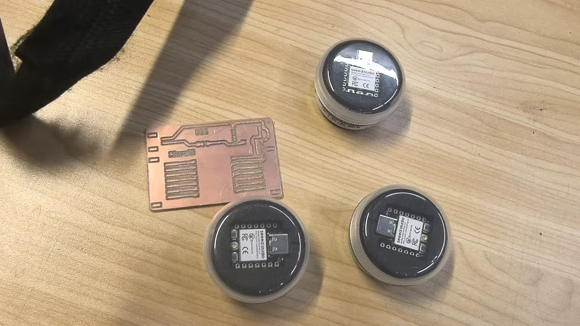
1. Independently develop development boards
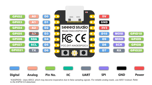
In this personal assignment, I made a small development board based on ESP32-C3 / XIAO-C3 . Its main goal is to provide stable power supply and lead out commonly used pins for easy subsequent connection of sensors, LED modules, and other peripherals.
1.1 Hardware Selection
This development board mainly includes the following hardware components:
| Module | Function |
|---|---|
| ESP32-C3 / XIAO-C3 主控 | is responsible for program execution, GPIO control, and communication |
| External 5V power input | Power the development board |
| Toggle Switch | Control power on/off |
| SS34 Schottky Diode | Reverse connection protection |
| 10 uF + 100 nF Capacitor | Power Supply Filtering and Stabilization |
| Power Indicator LED | Indicates whether the board is powered on |
| Pin Header / Socket Interface | Leads out GPIO, I2C, UART, SPI, and power supply |
The reason for choosing ESP32-C3 is its small size, low power consumption, and support for Wi-Fi/Bluetooth communication, making it suitable for subsequent IoT or interactive projects. For this week's assignment, I mainly used it to complete basic GPIO output verification.
1.2 Key Parameters
This development board focuses on bringing out the following interfaces:
- Power Supply: +5V, 3V3, GND
- GPIO: Used to connect LEDs, buttons, or other digital modules
- I2C: Used to connect modules such as OLEDs and sensors
- UART: Used for serial communication or debugging
- SPI: Used to connect high-speed peripherals
During design, try to follow basic circuit specifications, such as adding protection and filtering at the power supply inlet, providing GND and power pins next to interfaces, avoiding overly thin traces as much as possible, and checking for short-circuit issues with a multimeter before and after soldering.
2. Welding and Assembly
The PCB used in this welding is an iteratively optimized version of the initial design by the team. Compared to the original version, this board has adjusted the power traces, added test points, and made the pads more suitable for desktop CNC machining and manual soldering.
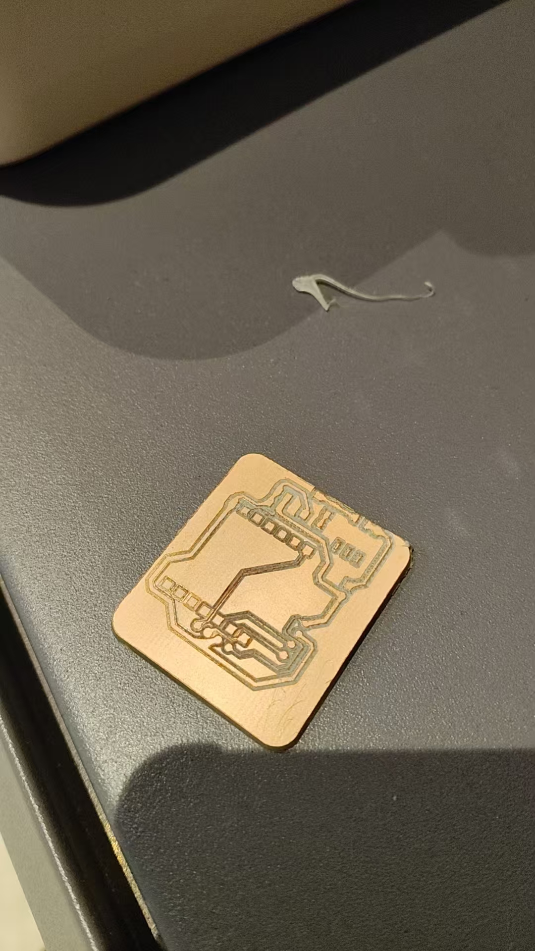
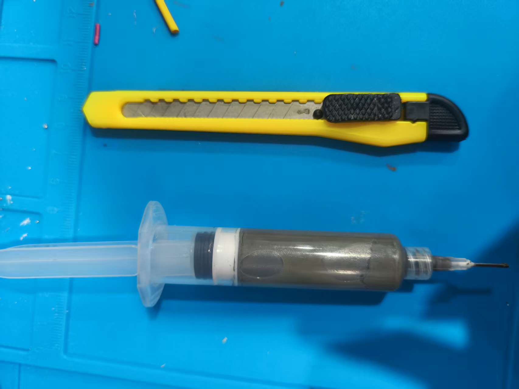
Since the machining accuracy of desktop CNC is relatively limited, there may still be copper wires that are not completely separated remaining at the edge of the tool path after actual carving. Therefore, before soldering, I use a utility knife to gently scrape along the edge of the tool path to remove burrs and residual copper shavings.
After cleaning is completed, first use a multimeter to measure the conduction of the bare board, focusing on checking whether the power supply and GND are short-circuited. After confirming that there are no obvious short circuits, apply solder paste, place components, and use a heating station for soldering.
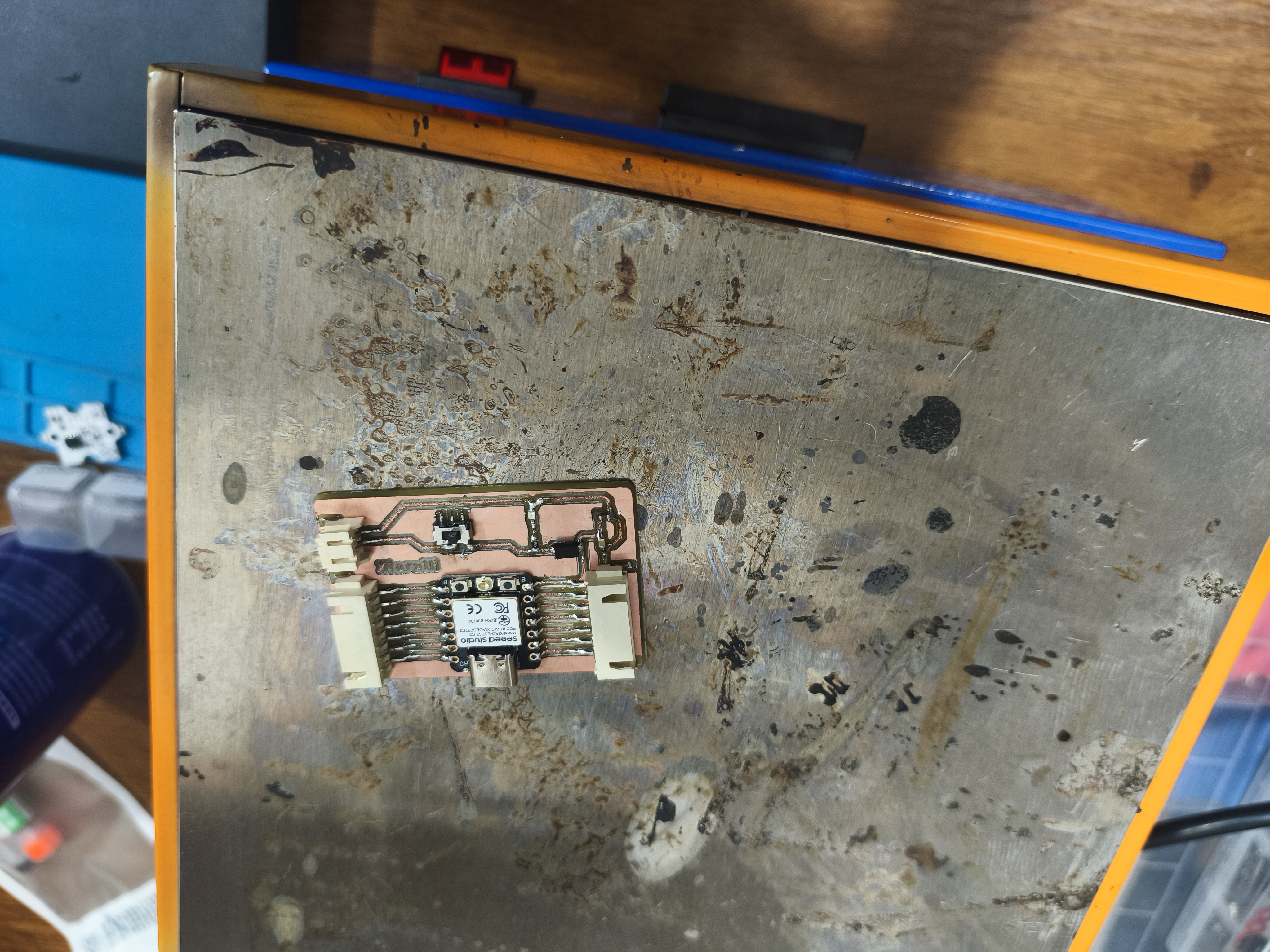
After welding is completed, insert the battery and toggle the power switch. If the power indicator lights up successfully, it indicates that the power supply section is working properly.
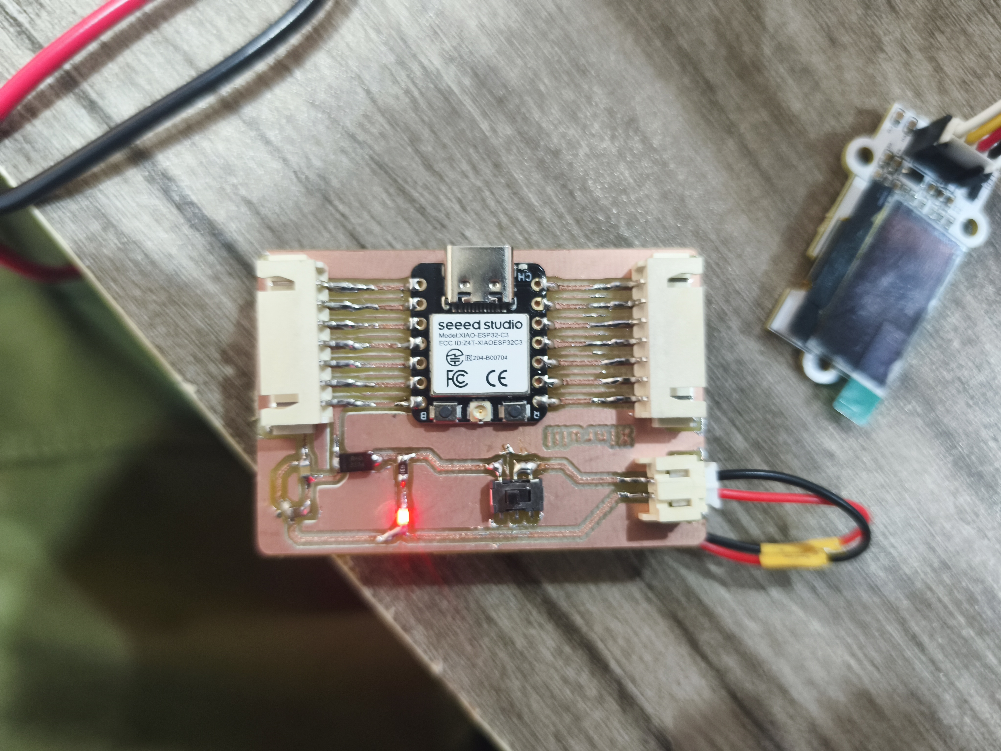
This step completes the soldering and assembly of the self-made copper-clad PCB. The long strip-shaped pads indeed reduce the alignment difficulty during actual soldering, ensuring sufficient soldering area even if there are slight deviations in engraving.
During the process, a problem was also encountered: initially, the power indicator light did not turn on. After troubleshooting, it was found that the copper shavings on the board surface were not cleaned thoroughly, and the remaining copper wires caused a local short circuit. After cleaning the copper shavings and rechecking, the power light returned to normal. This problem indicates that cleaning after PCB milling and multimeter testing are very important and should not be skipped directly to soldering.
3. Power Input Test
To first verify whether the power supply section of the development board is functioning properly, I connected a polymer battery as an external power source. After connecting the battery, I toggled the power switch on the board, and the power indicator light on the development board lit up red, indicating that power has been successfully input to the circuit board, and the switch, power circuit, and indicator module are all working properly.
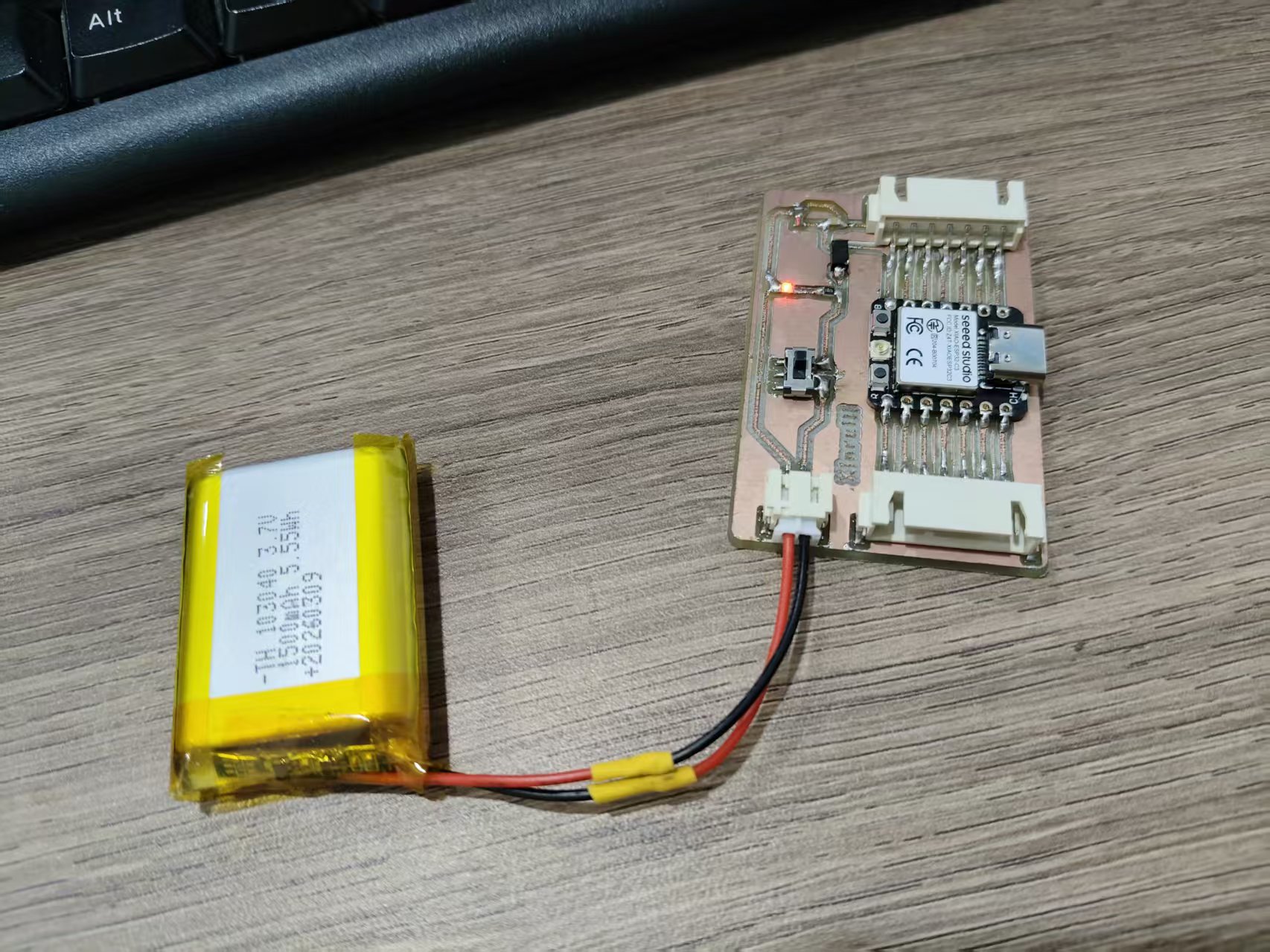
This step is a very important basic check before subsequent functional testing. If the power indicator does not light up, it is necessary to first troubleshoot the battery voltage, switch soldering, power input pads, diode orientation, and whether the power supply and GND are short-circuited. Only after confirming that the power supply is normal can the main control programming and peripheral testing continue.
4. Verification of the code burning function
This functional verification uses MicroPython . The advantage of MicroPython is its fast learning curve, allowing direct firmware flashing and test code execution via Thonny, making it suitable for quickly checking the basic functions of the development board.
4.1 Burn the MicroPython v1.28.0 firmware
I use Thonny to flash the MicroPython firmware onto the ESP32-C3 module. Before flashing, it is necessary to confirm the port, chip model, and driver status to avoid flashing failure caused by incorrect serial port selection.
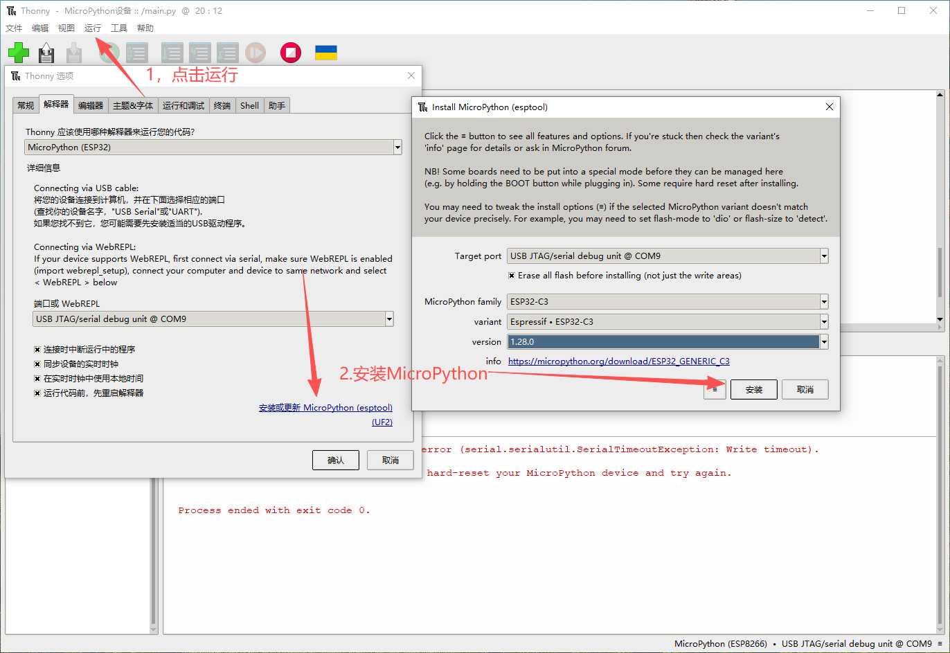
The burning process is roughly as follows:
- Connect the development board to the computer.
- Open Thonny and select the corresponding serial port.
- Select the MicroPython firmware corresponding to ESP32-C3.
- Start the burning process and wait for completion.
- After the burning is completed, reconnect the device and enter the MicroPython REPL.
4.2 Access Module
To verify the output function of the development board, I connected my self-developed GraftSense Piranha LED light module .
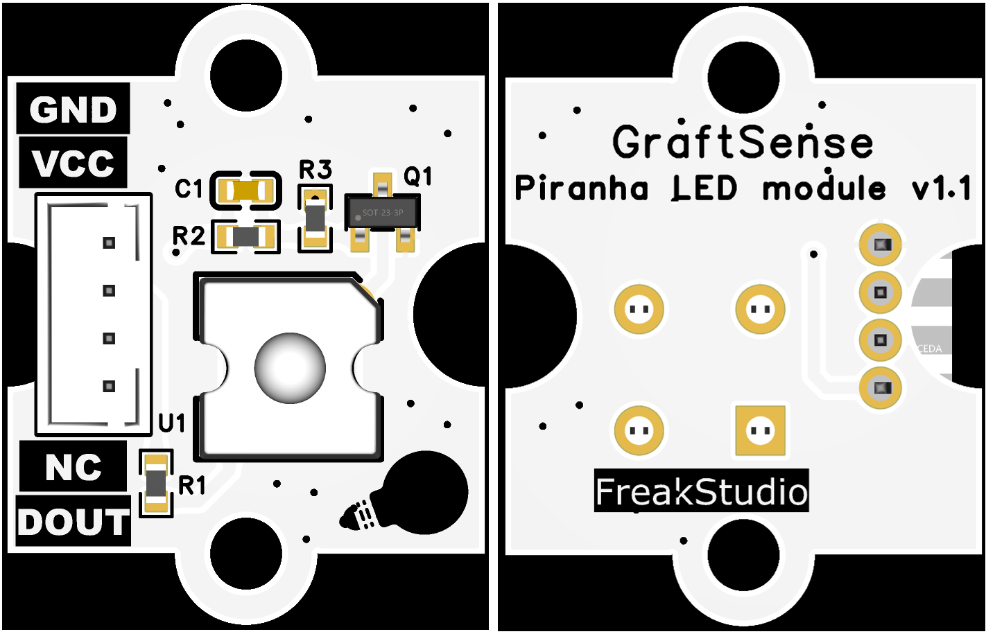
This module provides an output control interface DOUT. When DOUT inputs a high level, the transistor Q1 conducts, and the LED lights up; when DOUT inputs a low level, the transistor turns off, and the LED goes out.
Through this module, it is possible to verify whether the GPIO output of the development board is normal. If the program can control the DOUT high and low level changes, it indicates that the power supply, main control, and pin output of the development board are basically normal.
4.3 Run the test program
After the programming is completed, I run the LED test program to control the on and off of the external LED module through GPIO.
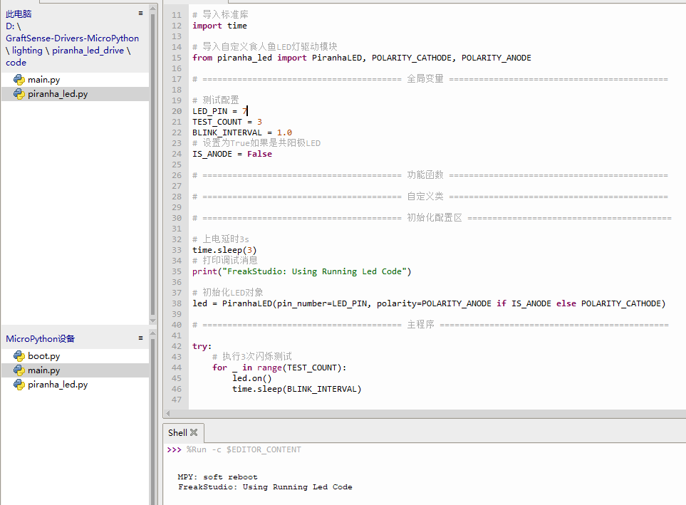
When the test program was run for the first time, the LED did not respond. After troubleshooting, it was found that the LED polarity configuration in the code was incorrect. After correcting the high and low level logic, the LED can light up and turn off normally according to the program.
This step verifies the basic functions of the development board:
- Power input is normal.
- The power switch and indicator light are normal.
- The main controller can burn MicroPython firmware.
- GPIO output can control external LED modules.
- The key circuits of the self-made PCB can function properly.
When the test program was run for the first time, the LED did not respond. After troubleshooting, it was found that the LED polarity configuration in the code was incorrect. After correcting the high and low level logic, the LED can turn on and off normally according to the program.
This step verifies the basic functions of the development board:
- Power input is normal.
- The power switch and indicator light are functioning normally.
- The main controller can burn MicroPython firmware.
- GPIO output can control external LED modules.
- The key circuits of the self-made PCB can operate normally.
5. Personal Assignment Summary
Through this week's individual assignment, I have fully experienced the entire process of PCB from design files, CNC milling, board surface cleaning, soldering and assembly to code verification. Compared to directly using off-the-shelf development boards, self-made PCBs are more likely to expose issues in actual manufacturing, such as copper residue, incomplete tool paths, pad offset, and incorrect program polarity configuration.
This practice has made me realize that the production of electronic products is not something that can be completed by just one single step, but rather a continuous process. During the design phase, processing capabilities need to be considered; after processing, careful inspection is required; before soldering, the board surface needs to be cleaned; and after programming, problems need to be troubleshooted by combining the code and hardware. Only when all these steps are completed can the circuit board truly transform from a "design document" into "functional hardware".
Attachment:
[!NOTE]
AI Assistance:
During the preparation of this documentation, ChatGPT \(GPT\-4\) was used as a language assistance tool.
It helped with sentence polishing and translation from Chinese to English to improve readability and clarity.