Week 11 - Networking and Communications
This week we start learning Networking and Communications . In embedded systems, a single development board can only perform local functions, while communication capabilities enable data exchange between multiple devices or allow devices to connect to the Internet to obtain information. Whether it is wired bus communication, Bluetooth, Wi-Fi, or network time synchronization and remote control, they all essentially involve data transfer between nodes according to a certain protocol.
A communication system typically involves several key concepts: Node, Address, Protocol, and Message. A node is a device that participates in communication, an address is used to distinguish different devices, a protocol specifies how data is sent and received, and a message is the actual content being transmitted.
Group assignment:
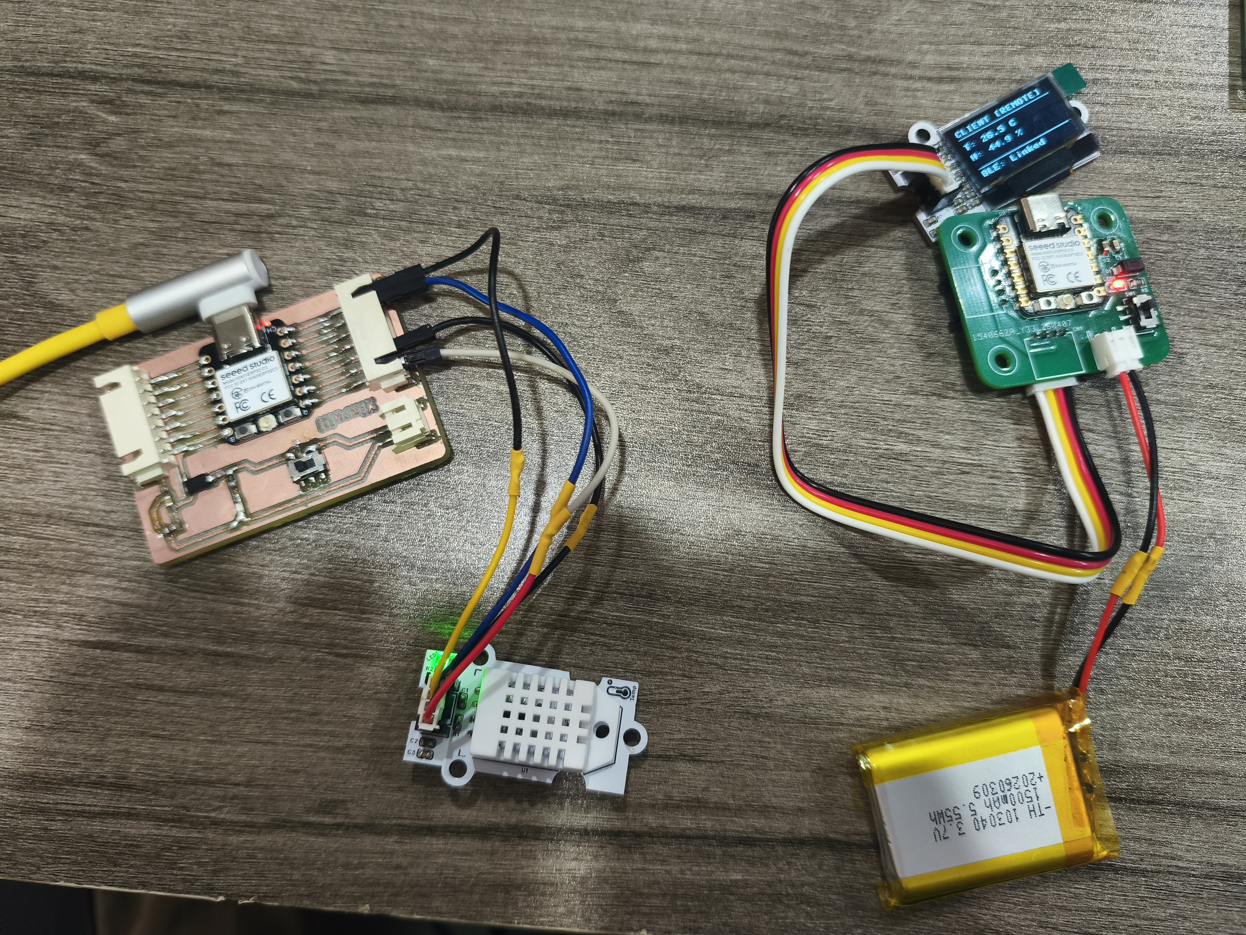
The group assignment requires sending messages between two projects. This time, we use two XIAO ESP32-C3 development boards to achieve the transmission of temperature and humidity data from the sender to the receiver through BLE Bluetooth communication. The sender collects DHT22 temperature and humidity data and sends it through the BLE GATT service; the receiver scans and connects to the sender, subscribes to data notifications, and then displays the temperature and humidity on the OLED screen.
Individual assignment:
Individual assignment requires designing, fabricating, and connecting wired or wireless nodes with network or bus addresses, and including local input or output devices. This time, I used the Wi-Fi functionality of the XIAO ESP32-C3 to create a NTP network synchronization clock. The development board, as a wireless network node, connects to Wi-Fi, obtains standard time from a network server via the NTP protocol, and displays time information on a local OLED screen.
Overall, the focus of this week is not on implementing complex large-scale networks, but on understanding how devices establish connections, how to distinguish nodes, how to send and receive data, and how to convert network data into local input/output functions.
Group Assignment
Group Assignment Page: https://fabacademy.org/2026/labs/chaihuo/docs/week11/msc/week11_group_assignment
1. BLE Dual Node Communication Experiment
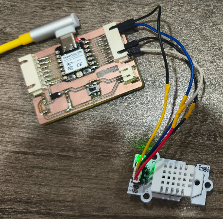
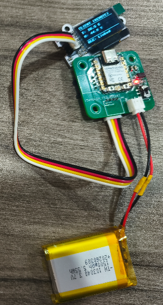
This group assignment uses two XIAO ESP32-C3 development boards to complete BLE Bluetooth communication. The experimental goal is to send messages between two projects: one board serves as the sender, reading data from the DHT22 temperature and humidity sensor; the other board serves as the receiver, displaying the received data on the OLED screen after receiving it.
BLE (Bluetooth Low Energy) is suitable for short-range, low-power data transmission. Different from traditional serial communication, which is not simply one TX paired with one RX, BLE organizes data through services and characteristics. The receiving end can connect to the sending end and subscribe to characteristic notifications to receive data in real time.
2. Communication Roles and Addresses
In this experiment, the roles of the two boards are as follows:
| Node | Role | Function | Local Device |
|---|---|---|---|
| Transmitter Host / Peripheral | BLE Peripheral Server | Collect temperature and humidity and broadcast services | DHT22 Sensor |
| Receiver Client / Central | BLE Central Device | Scan, connect, and receive data | OLED Display |
The sender exposes its service information through BLE broadcasting, while the receiver discovers the device by scanning and determines whether to connect to the target node based on the service UUID. Here, the UUID is equivalent to the address and identification marker in BLE communication, used to distinguish different services and data channels.
This temperature and humidity data is transmitted using a fixed characteristic UUID. Temperature uses the int16 format, and humidity uses the uint16 format. To retain two decimal places, the data is multiplied by 100 and converted to an integer before transmission, and then divided by 100 at the receiving end to restore the actual temperature and humidity.
The advantage of this approach is that the data is more compact and it also avoids the additional overhead caused by directly transmitting strings.
3. Project Structure
This BLE communication project is divided into two parts: the transmitting end and the receiving end, and simultaneously uses the OLED driver and the BLE low-level library.
├── host/                    # 主机代码文件夹
│   ├── main.py              # 主机主程序入口
│   ├── dht_task.py          # DHT22传感器采集任务
│   ├── oled_task.py         # 主机OLED显示任务
│   └── ble_peripheral_task.py # BLE从机广播通信任务
├── client/                  # 客机代码文件夹
│   ├── main.py              # 客机主程序入口
│   ├── oled_task.py         # 客机OLED显示任务
│   └── ble_central_task.py  # BLE主机扫描连接任务
├── ssd1306_driver/code/ssd1306.py   # OLED通用驱动文件
└── aioble/                          # BLE蓝牙底层驱动
This structure separates acquisition, display, and communication, making the code easier to debug. The transmitting end mainly focuses on sensors and broadcasting, while the receiving end mainly focuses on scanning connections and data display.
4. Transmitter Design
The sender remains in passive communication mode throughout. It does not actively search for other devices, but is responsible for collecting sensor data, initiating BLE broadcasts, establishing GATT services, and waiting for the receiver to connect.
The transmitting end is connected to the DHT22 temperature and humidity sensor: DHT22 sensor: DATA data pin is connected to GPIO20
The basic workflow of the sender is as follows:
- Initialize the DHT22 sensor.
- Initialize BLE services and characteristics.
- Start BLE broadcasting and wait for the receiver to connect.
- Periodically read temperature and humidity data.
- Convert the data to integer format.
- Actively pushed to the receiving end via BLE notify.
The key point here is notify. It allows the sender to proactively notify the receiver when data changes, eliminating the need for the receiver to continuously poll for updates, thereby improving communication efficiency.
5. Receiver Design
The receiver remains in the active communication mode throughout. It is responsible for scanning surrounding BLE devices, actively initiating a connection after finding the target service, and subscribing to temperature and humidity data notifications. After receiving the data, the receiver will parse the data and refresh the OLED screen.
The receiving end is connected to an OLED screen:
- OLED Screen:
SDAConnects toGPIO6 - OLED Screen:
SCLConnects toGPIO7 - The receiving end has no external sensors and is only responsible for receiving and displaying data
The basic workflow of the receiving end is as follows:
- Initialize the OLED display.
- Start BLE scanning.
- Find the sender based on the service UUID.
- Connect the sender.
- Subscribe to the notify of temperature and humidity characteristic values.
- Receive and parse data.
- Display temperature and humidity on the OLED screen.
Through this part of the experiment, we completed the message passing between the two projects: the sender project collects environmental data, and the receiver project receives and displays the data.
6. Summary of Group Assignment
Through this BLE dual-node communication experiment, I have understood the relationship between the central device and the peripheral device in BLE communication. The sender does not simply "throw out the data" directly, but first establishes services and characteristic values; the receiver does not receive data randomly either, but needs to scan, identify UUIDs, connect, and subscribe to notifications.
Compared to serial communication, the process of BLE is more complex, but its advantages are wireless, low power consumption, and suitability for organizing data among multiple devices through services and characteristic values. This experiment also helped me understand the significance of "nodes with addresses" in wireless communication: device names, service UUIDs, and characteristic UUIDs can all assist the receiving end in identifying target nodes and data types.
Individual Assignment
1. NTP Network Synchronized Time Display
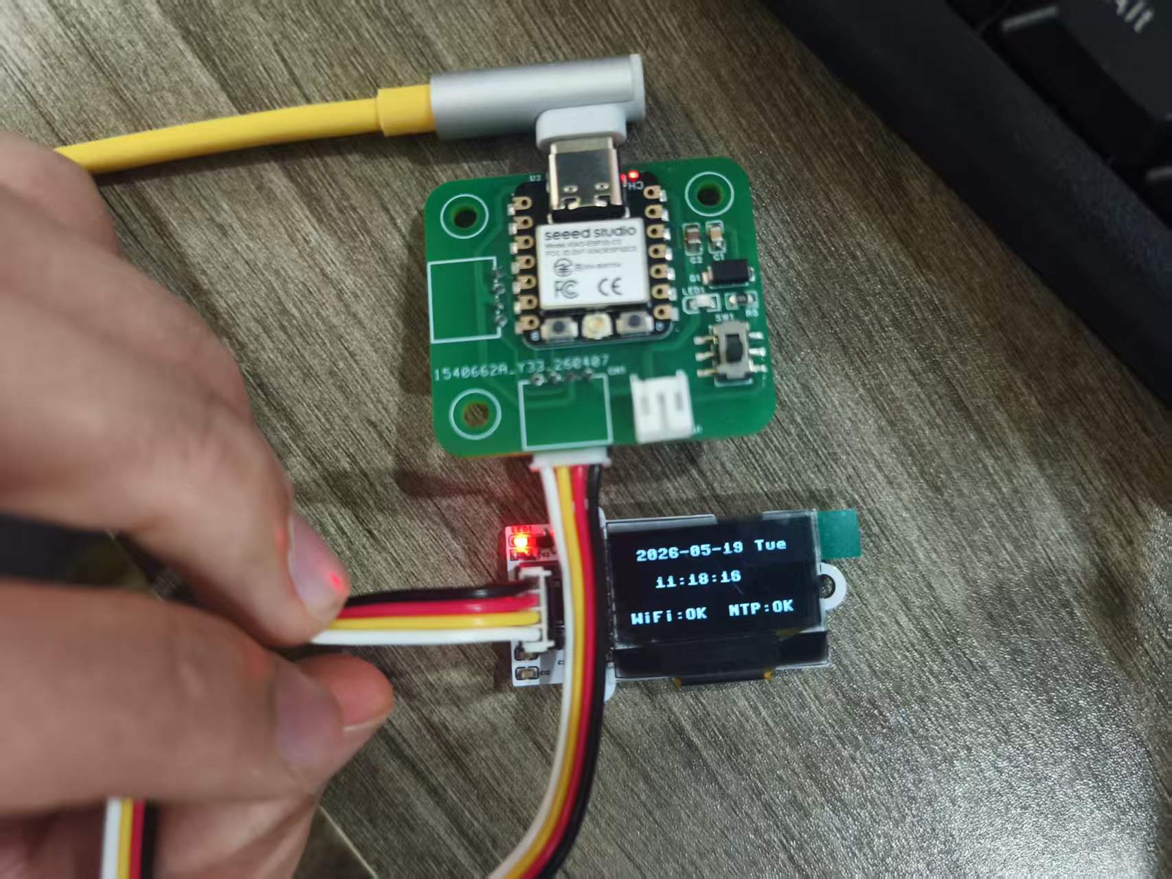
In my personal assignment, I chose to create a network synchronized time display . The XIAO ESP32-C3 has Wi-Fi capabilities, so it can act as a wireless network node to connect to a router and obtain standard time from a network server via the NTP protocol.
This project includes:
- A wireless network node: XIAO ESP32-C3;
- One network address source: Wi-Fi network and NTP server;
- A local output device: OLED display;
- A Communication Protocol: Wi-Fi + NTP.
This way, it meets the requirement of "connecting nodes with network addresses and including local input/output devices" in this week's individual assignment.
2. Project Structure
ntp_clock/
├── main.py          # 主程序
├── wifi_task.py     # WiFi 连接
├── ntp_task.py      # NTP 时间同步(UTC+8)
└── oled_task.py     # OLED 显示
Modularization structure makes the responsibilities of each part clearer:
wifi_task.pyis responsible for connecting to the wireless network;ntp_task.pyis responsible for obtaining and parsing network time;oled_task.pyis responsible for displaying time and status;main.pyis responsible for calling each module and controlling the main loop.
3. Wi-Fi Network Connection
In wifi_task.py, you need to configure the Wi-Fi name and password:
After the ESP32-C3 connects to Wi-Fi, it will obtain a local network IP address from the router. This IP address is the device's network identity within the local area network, and other devices can identify it through the network address.
After a successful Wi-Fi connection, the program will continue with Network Time Protocol (NTP) time synchronization. If the Wi-Fi connection fails, the OLED will not be able to display the correct network time.
4. Network Time Protocol (NTP) Time Synchronization Logic
NTP (Network Time Protocol) is a network time protocol that allows devices to obtain standard time from time servers on the Internet. For development boards without a real-time clock module, NTP is a very convenient way to synchronize time.
ntp_task.py module mainly performs the following tasks:
- Configure the Network Time Protocol (NTP) server address;
- Initiate a time synchronization request to the server;
- Receive the UTC standard time returned by the server;
- Convert UTC time to UTC+8, which is Beijing Time;
- Parse information such as year, month, day, weekday, hour, minute, and second;
- Provide the formatted time to the OLED display module.
The "network node address" in the NTP project is mainly reflected in two aspects: one is the local area network IP address obtained by the ESP32-C3 after connecting to Wi-Fi, and the other is the NTP server address. The development board accesses the server through the network address and then converts the remote time data into local display content.
5. OLED Display Implementation
oled_task.py module is responsible for displaying the parsed time and status information on the OLED screen. The displayed content includes:
- Date and day of the week, e.g.:
2026-05-18 Tue - Current time, for example:
11:10:16 - Network Status:
WiFi:OK - Time Synchronization Status:
NTP:OK
The status display of OLED is very helpful for debugging. If Wi-Fi display fails, it indicates a problem during the network connection phase; if Wi-Fi is normal but NTP fails, it indicates a problem with network time requests or server access.
6. Communication Process
The data flow of the entire personal project is as follows:
The ESP32-C3 first connects to Wi-Fi, then accesses the NTP server to obtain the standard time. After obtaining the time, the program converts the UTC time to Beijing time and displays it locally via the OLED.
Although this project does not involve the interconnection of multiple local development boards, it uses wireless network communication and exchanges data with a remote server, so it is also a network node communication application.
7. Debugging and Results
During debugging, I mainly focus on two states:
- Whether Wi-Fi is successfully connected.
- Whether NTP time synchronization was successful.
When the OLED displays WiFi: OKand NTP: OKat the same time, it means that the development board has successfully connected to the network and completed time synchronization. The screen can display the date, week and time in real time, indicating that the process from network communication to local output has been connected.
Through this experiment, I found that the debugging of communication projects is not quite the same as that of ordinary sensor projects. Sensor projects mainly check wiring and pins, while network communication projects also need to check issues such as Wi-Fi name, password, network environment, server access, and time zone conversion.
8. Summary
Through this week's assignments, I completed communication exercises at two different levels. In the group assignment, two XIAO ESP32-C3 boards sent and received temperature and humidity messages via BLE, with the focus on wireless communication between devices; in the individual assignment, a single XIAO ESP32-C3 board connected to the network via Wi-Fi and used NTP to obtain time, with the focus on communication between the development board and the network server.
These two experiments have enabled me to understand the common logic of communication systems: first establish a connection, then confirm the address or service identifier, and finally send and receive data according to the protocol. Whether it is the UUID in BLE or the IP address and NTP server address in Wi-Fi, they essentially allow devices to know "who to communicate with" and "what data to transmit".
Attachment:
[!NOTE]
AI Assistance:
During the preparation of this documentation, ChatGPT (GPT-4) was used as a language assistance tool.
It helped with sentence polishing and translation from Chinese to English to improve readability and clarity