Week 6 - Electronic Design
This week we start learning Electronics Design . In digital manufacturing projects, electronic circuits are an important part that connects software, sensors, actuators, and physical structures. By designing circuit boards, microcontrollers can be stably connected to external devices, thereby achieving functions such as Data Acquisition, display, control, and communication.
The core of electronic design is not just "connecting components"; it also includes understanding circuit principles, selecting appropriate components, drawing schematics, designing PCB traces, and using test instruments to verify whether the circuit is working properly. Therefore, this week's learning focus can be divided into two parts: one is to familiarize with the electronic test equipment in the laboratory, and the other is to use EDA tools to complete the design of a circuit board.
Group assignment:
The group assignment mainly involves familiarizing ourselves with the test equipment in the laboratory, such as multimeters, DC power supplies, signal generators, oscilloscopes, and logic analyzers. By observing the device panels, understanding the key buttons, and basic functions, we learn how to measure voltage, current, waveforms, and communication signals. Meanwhile, we use these devices to observe the operating status of the microcontroller circuit board and record the changes in input and output voltage, current, and signals.
Individual assignment:
Individual assignments mainly involve trying out different EDA (Electronic Design Automation) tools and selecting one of them to complete the circuit board design. The design content needs to include a controller, an input interface or input device, an output device, and basic communication functions. Finally, the schematic diagram, PCB layout, and circuit board renderings need to be completed, and the design files uploaded to the personal webpage.
Overall, the focus of this week is to establish the basic process from "circuit idea" to "PCB design file": first understand the circuit function, then draw the schematic diagram using EDA software, subsequently complete PCB layout and routing, and finally verify whether the circuit works properly through test equipment.
Group Assignment
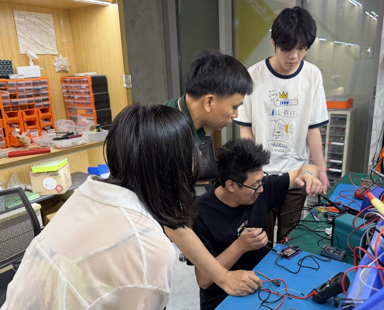
In this week's group assignment, we mainly familiarized ourselves with common electronic test equipment in the laboratory and used them to observe the working states of single-chip microcomputers and external devices. The equipment we came into contact with this time includes:
- Multimeter
- DC Power Supply
- Signal Generator
- Oscilloscope
- Logic Analyzer
These devices play different roles in electronic debugging. Multimeters are suitable for measuring static voltage, current, and resistance; oscilloscopes are suitable for observing analog or digital waveforms that change over time; and logic analyzers are more suitable for analyzing digital communication data, such as I2C, SPI, UART, etc.
Group Assignment Page:Week 6 — Group Assignment: Embedded Programming | FAB26 - ChaiHuo Makerspace 2026
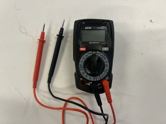
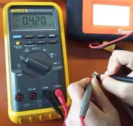
1. Multimeter
A multimeter is the most fundamental testing tool in electronic experiments, primarily used to measure voltage, current, resistance, and continuity. When debugging a circuit board, a multimeter is usually the first tool to be used because it can quickly determine whether the circuit is powered properly, whether there is a short circuit, and whether components are connected.
The common functions of a multimeter are as follows:
| Function | Function | Usage Scenarios |
|---|---|---|
| DC Voltage DCV | Measure the DC voltage in the circuit | Check if the 5V and 3.3V power supplies are normal |
| Alternating Current Voltage ACV | Measure AC voltage | Check AC power or adapter output |
| Current Measurement | Measure the operating current of the circuit | Estimate power consumption and check for overload |
| Resistance Measurement | Measure the resistance value | Check the resistor model or line impedance |
| Conduction Test | Determine whether two points are connected | Check for welding, short circuits, or broken wires |
1.1 Voltage Measurement (Voltage)
In electronic circuit debugging, voltage measurement is most commonly used to check whether the power supply is normal. For example, a microcontroller development board usually requires a 5V or 3.3V power supply. If the supply voltage is unstable, the circuit may fail to start or experience abnormal resets during operation.
When measuring voltage, the multimeter needs to be connected in parallel with the circuit under test. The black probe is connected to GND, and the red probe is connected to the power supply or signal point to be measured.
1.2 Current Measurement (Current)
Current measurement can help us understand the power consumption of a circuit and also determine whether there is an overload issue in the circuit. Different from voltage measurement, current measurement requires connecting a multimeter in series to the circuit, allowing current to flow through the multimeter.
If the current range is selected incorrectly, or if the current range is directly connected in parallel across the power supply, it may cause a short circuit. Therefore, special attention should be paid to the wiring method when using the current range.
1.3 Resistance Measurement (Resistance)
A multimeter can also be used to measure resistance. When measuring resistance, it is necessary to cut off the power supply to the circuit before taking the measurement to prevent the voltage in the circuit from affecting the reading or even damaging the multimeter. Generally, switch the multimeter to the resistance range, touch the two ends of the resistor with the two test leads respectively, and then the resistance value can be read.
During actual circuit debugging, resistance measurement can be used to confirm whether the resistance value of a resistive component is correct, and can also be used to check whether there are abnormal short circuits or open circuits in the circuit. For example, after soldering is completed, if the resistance between two points is close to 0 Ω, it may indicate that they are shorted; if the resistance of a circuit that should be connected is very large, there may be a cold solder joint or a broken wire.
2. DC Power Supply
DC power supplies are used to provide stable voltage and current to circuits. Compared to directly using USB or batteries, laboratory DC power supplies allow manual setting of output voltage and current limit values, making them safer when debugging new circuit boards.
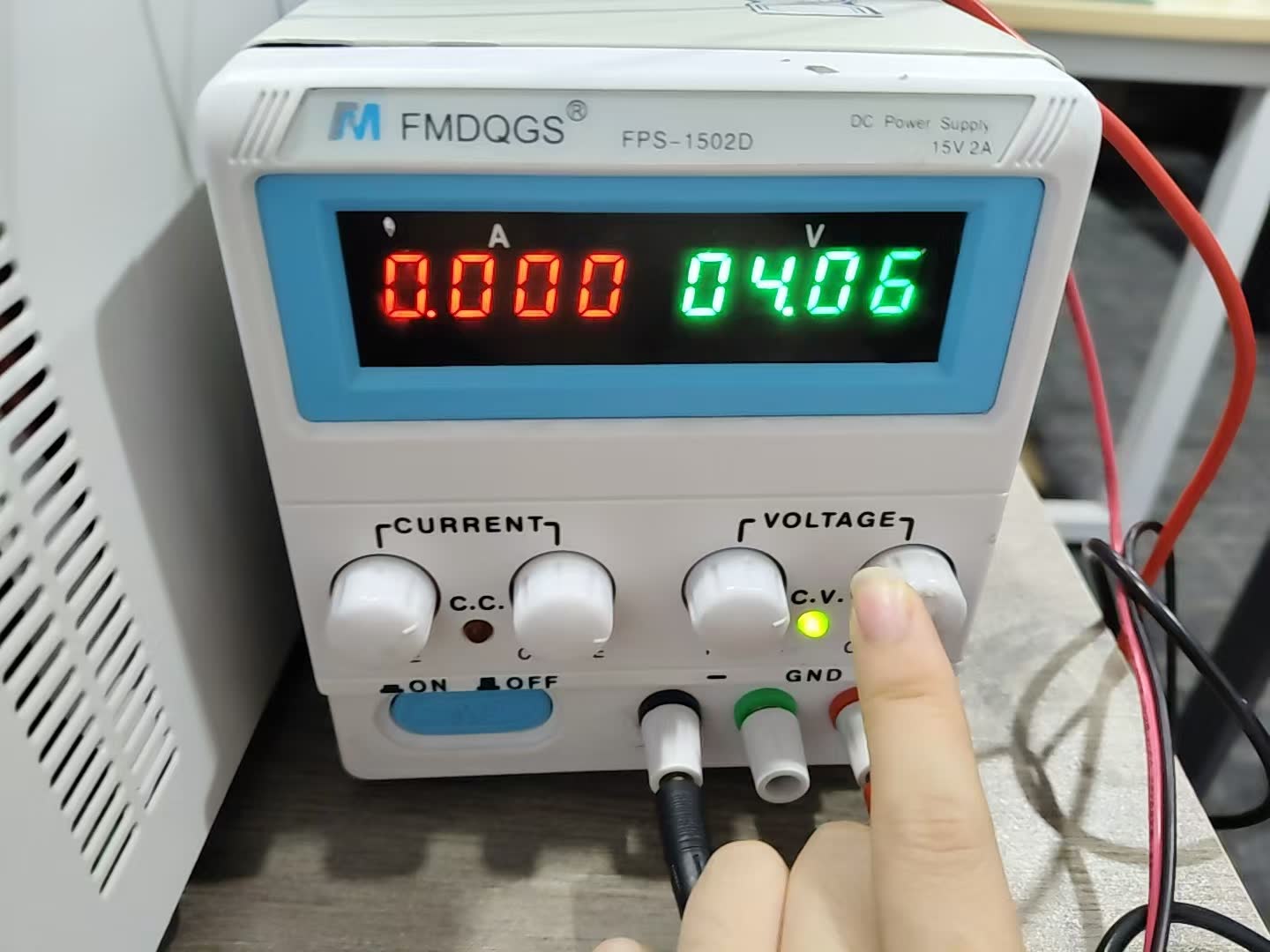
Common key controls for DC power supplies include:
| Component / Button | Function |
|---|---|
| Voltage adjustment | Set output voltage |
| Current adjustment | Set the maximum output current |
| Output Switch | Controls whether to output power |
| Voltage Display Screen | Display the current output voltage |
| Current Display Screen | Display the current load current |
| Positive and negative output terminals | Connect the VCC and GND of the circuit under test |
When debugging a single-chip microcomputer circuit, you can first set an appropriate current limit value. If there is a short circuit in the circuit, the power supply will enter the current limit state to prevent components from being burned out.
3. Signal Generator (Signal Generator)
A signal generator can output signals with specific frequency, amplitude, and waveform, such as sine wave, square wave, triangular wave, etc. It is commonly used to test the response of a circuit to input signals.
In this study, we mainly focus on square wave signals. Square waves can simulate the high and low level changes in digital circuits, and can also be used to test oscilloscope triggering, frequency measurement, and PWM waveform observation.
Common settings for signal generators include:
| Setting Item | Description |
|---|---|
| Waveform | Select the waveform type, such as Sine, Square, Triangle |
| Frequency | Set Output Frequency |
| Amplitude | Set Output Amplitude |
| Offset | Set DC Offset |
| Output | Turn on or off the signal output |
By outputting a stable square wave through a signal generator and then observing the waveform with an oscilloscope, we can better understand the period, frequency, duty cycle, and voltage amplitude of the signal.
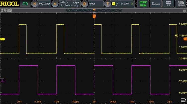
4. Oscilloscope
An oscilloscope is used to observe the waveform of an electrical signal changing over time. Unlike a multimeter, which can only display a state at a certain moment or an average state, an oscilloscope can show the changing process of a signal, making it very suitable for analyzing PWM, serial waveforms, clock signals, and sensor outputs.
Common controls of an oscilloscope are as follows:
| Control Item | Function |
|---|---|
| CH1 / CH2 | Select different input channels |
| Vertical Scale | Adjust the voltage display ratio |
| Horizontal Scale | Adjust time display scale |
| Trigger Level | Set the trigger level to ensure stable display of the waveform |
| Run / Stop | Start or pause waveform acquisition |
| Measure | Automatically measure parameters such as frequency, voltage, and period |
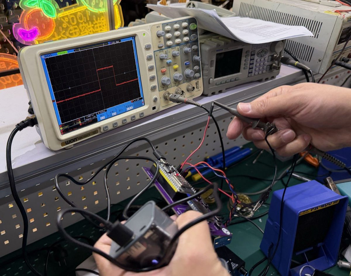
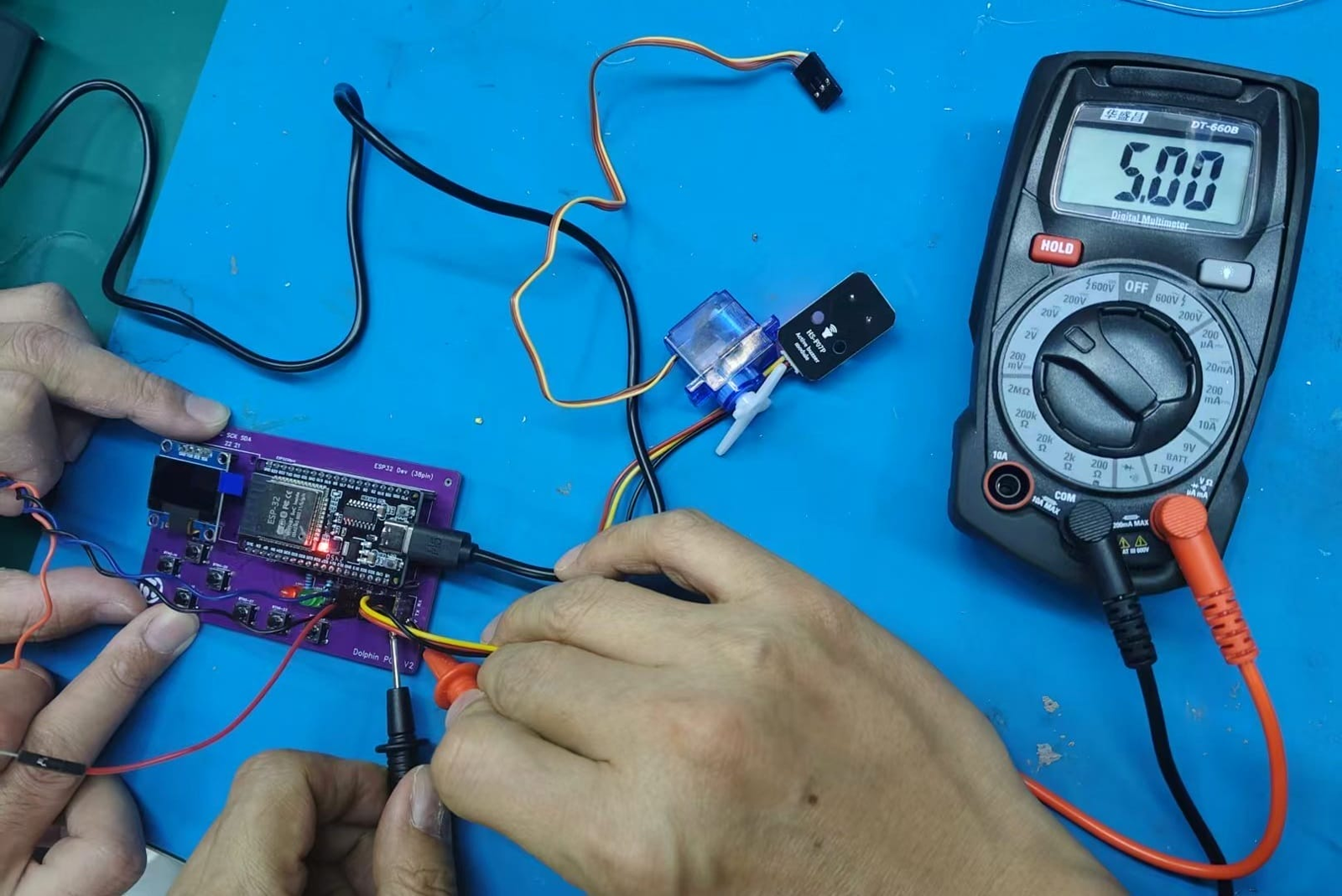
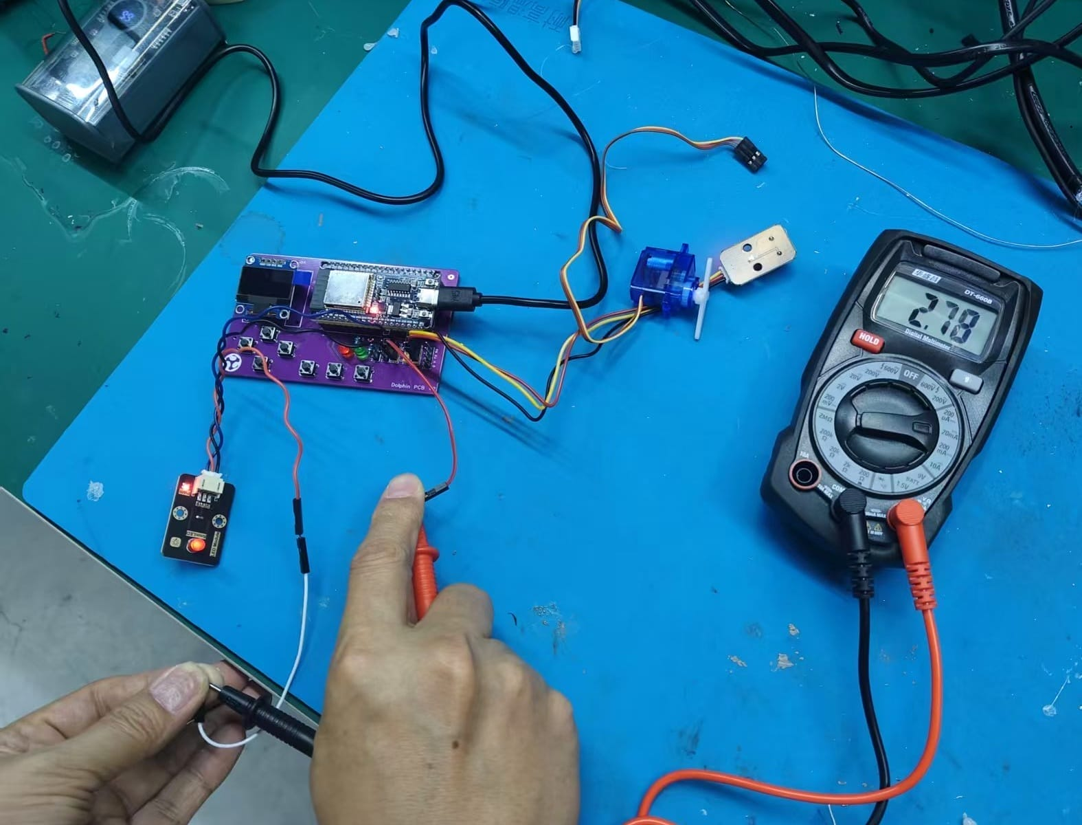
This time, we will connect the ESP32 to a servo motor and program it to rotate the servo to 90°, 0°, and -90°. The servo control signal is essentially a PWM signal, so an oscilloscope can be used to observe its pulse width changes.
As can be seen from the oscilloscope, when the target angle changes, the high-level duration of the control signal also changes. This experiment has allowed me to more intuitively understand that the PWM signal is not simply a "switch," but rather conveys control information through pulse width.
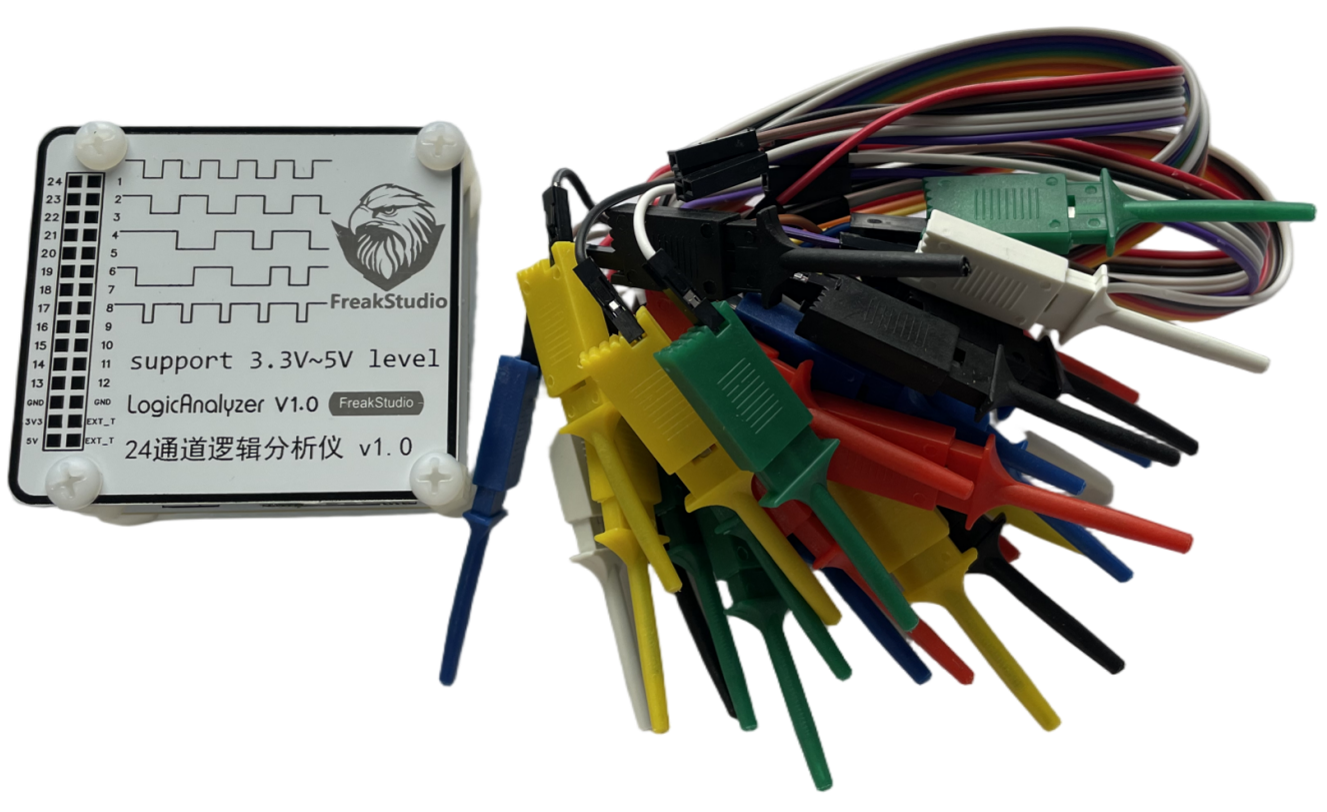
5. Logic Analyzer
Logic analyzers are mainly used to analyze digital signals. Unlike oscilloscopes, which focus on the details of voltage waveforms, logic analyzers identify signals as high and low levels and then display them in chronological order. Therefore, they are well-suited for analyzing communication protocols, such as UART, I2C, and SPI.
The common usage process of a logic analyzer is as follows:
- Connect GND to the common ground of the circuit under test.
- Connect the analyzer channel to the digital signal line that needs to be observed.
- Set the sampling rate and protocol type in the software.
- Start signal acquisition.
- Use the protocol parsing function to view the specific data content.
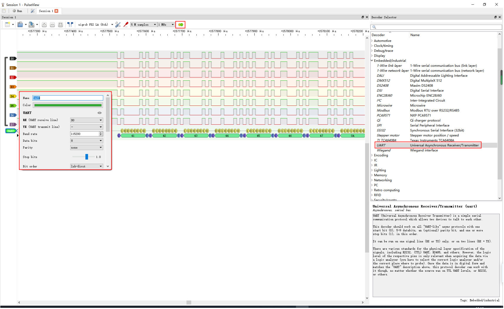
For example, in UART communication, a logic analyzer can directly parse the content of transmitted and received ByteDance; in I2C communication, it can display the device address, read/write bit, and data ByteDance. This is very helpful for debugging sensor communication.
6. Summary of Group Experiment
Through this group experiment, I have gained a clearer understanding of the usage scenarios of different test equipment. Multimeters are suitable for basic inspections and can quickly determine whether power supply and connections are normal; oscilloscopes are suitable for observing dynamic signals and can show the process of signals such as PWM changing over time; logic analyzers are more suitable for analyzing digital communication data.
These tools are very important when designing circuit boards on your own in the future. After the design is completed, you cannot rely solely on software checks; you also need to confirm whether the voltage, current, and communication signals meet expectations through actual measurements.
Individual Assignment
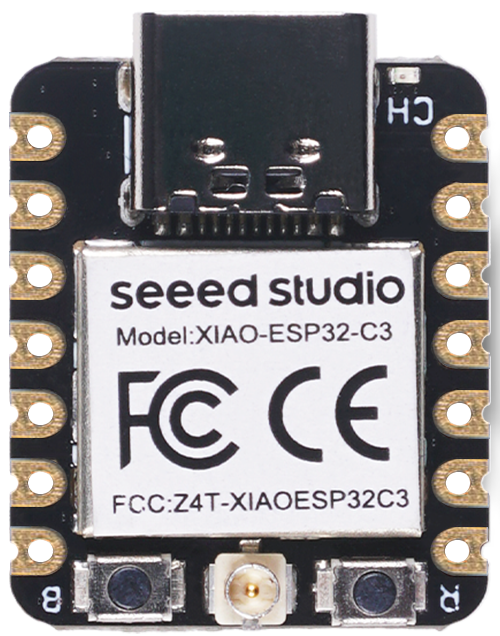
This week's individual assignment requires using EDA tools to design a development board that can communicate interactively with a microcontroller. It needs to include a controller, input devices or input interfaces, output devices, and communication capabilities. My design direction is to create an expansion board based on the Seeed Studio XIAO series of main controllers, which will facilitate continued use in input devices, output devices, and the final project.
I named this board GraftPort-XIAO Expansion Board . Instead of directly fixing a specific sensor onto the board, it creates a small expansion baseboard around the XIAO main controller: on one hand, it provides external power supply, power switch, and power indicator; on the other hand, it leads out commonly used I2C, UART, and power interfaces, facilitating the connection of Grove sensors, OLED/LCD displays, or other serial modules.
1. EDA Tool Selection
Before starting the design, I first familiarized myself with several common EDA (Electronic Design Automation) tools. EDA tools are mainly used for drawing circuit schematics, designing PCBs, managing components and packages, and exporting manufacturing files for production.
| EDA tools | Type | Features | Common Usage Scenarios |
|---|---|---|---|
| KiCad | Open Source Software | Free and open source, fully functional, with an active community | Open source hardware, teaching, maker projects |
| Eagle | commercial software | It has a longer history and a relatively simple interface | Small circuit design, early maker projects |
| Altium Designer | commercial software | Powerful, suitable for complex designs | Professional Electronic Engineering, Enterprise-level PCB |
| JLCEDA (EasyEDA) | Online/Desktop Tools | Rich component library, capable of interfacing with PCB production | Rapid prototyping, small batch production, teaching |
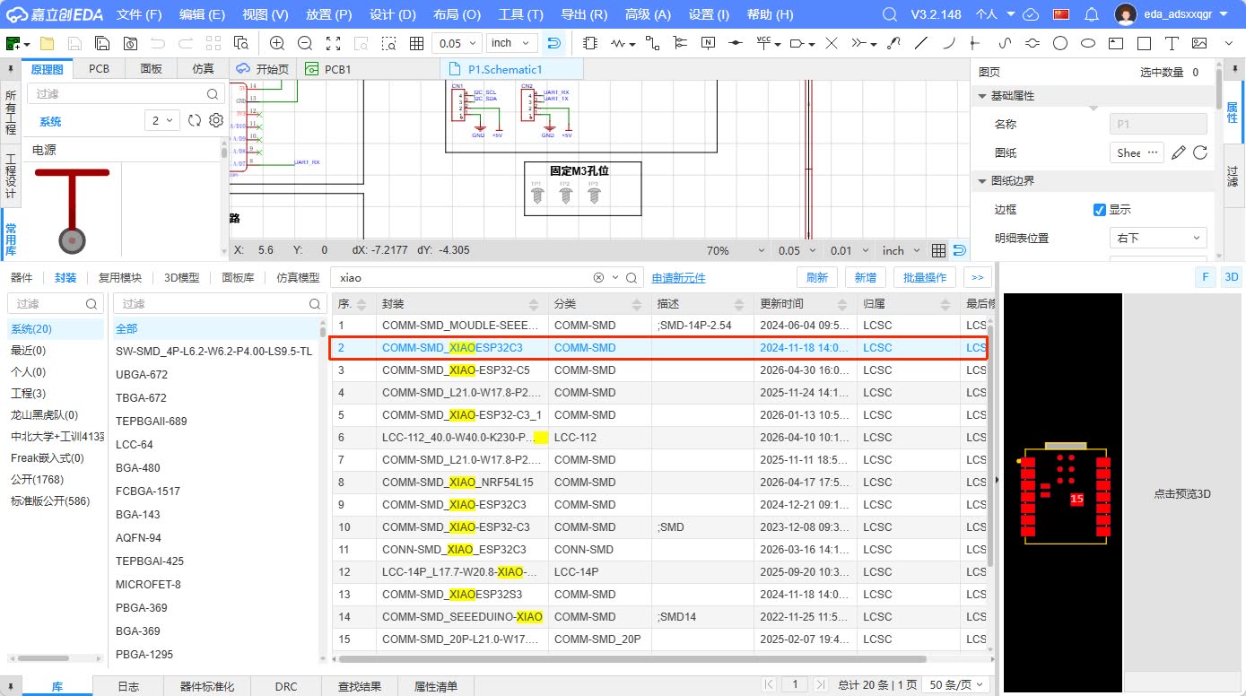
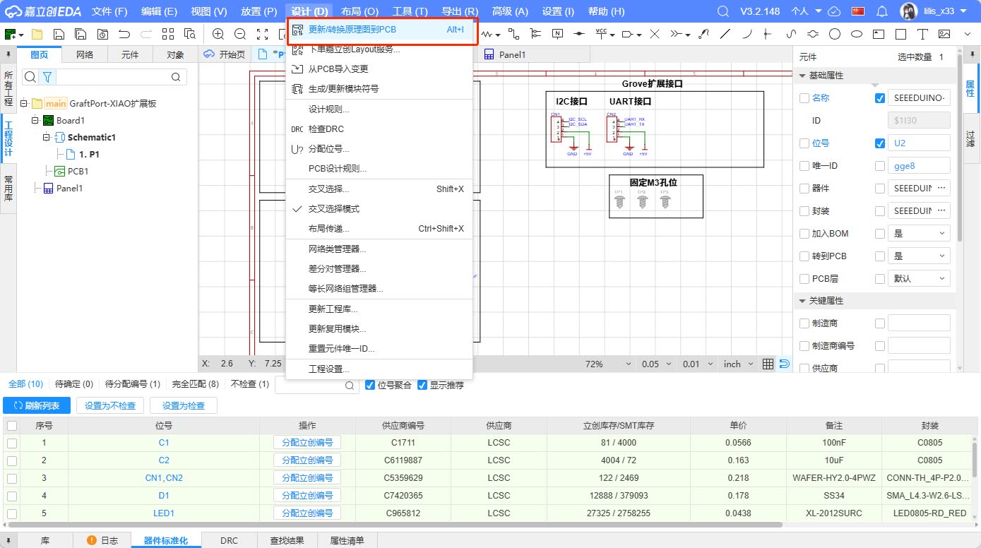
For this assignment, I chose to use JLCPCB EDA / EasyEDA. There are three main reasons: First, its component library and package library are relatively complete, making it user-friendly for beginners; Second, the processes of schematic, PCB, and 3D preview are well-connected; Third, it can conveniently export production files, making it suitable for continued use in the subsequent production cycle of electronic products.
Through this design, I have understood that EDA design is not just about connecting wires, but also about considering four things simultaneously:
- Are the electrical connections in the schematic diagram correct?
- Whether the package of each component matches the real component.
- Is the location of components on the PCB convenient for soldering, plugging and unplugging, and testing?
- Are the traces of the power supply, GND, and communication lines reliable?
2. Design Objectives and Function Planning
I hope this expansion board can serve as the base board for subsequent projects, so the design goal is not to create a particularly complex circuit, but rather to build an interface board that is stable, clear, and easy to expand.
This design needs to meet the following functions:
| Assignment Requirements | My implementation approach |
|---|---|
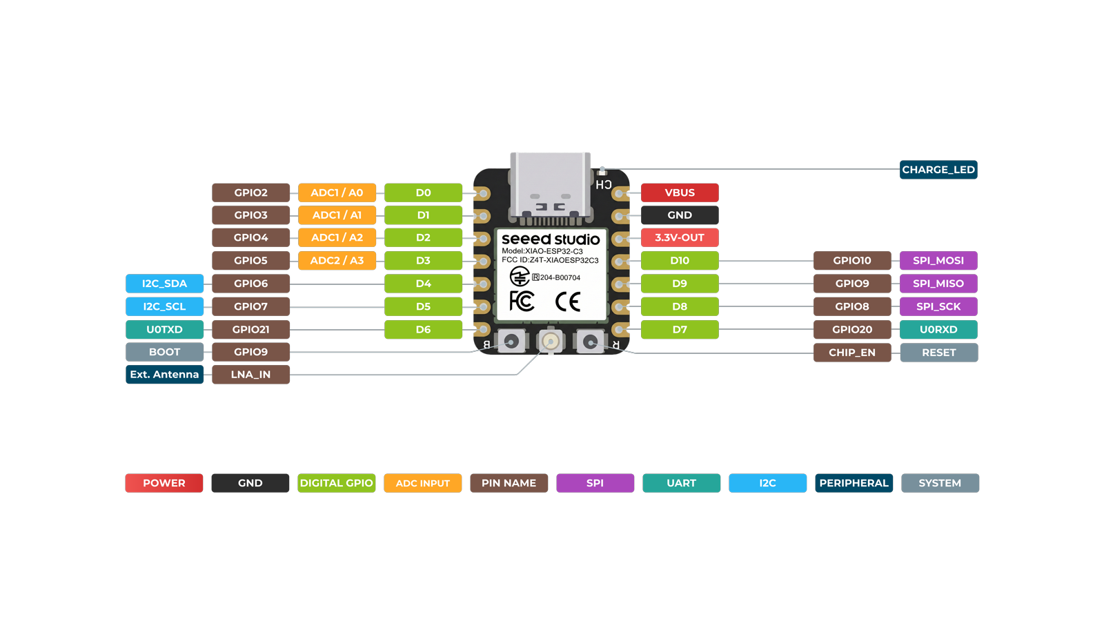
| Controller | Using the Seeed Studio XIAO series development boards as the main controller, it is compatible with models such as XIAO RP2040 / XIAO ESP32-C3 |
| Input device or input interface | Reserved Grove I2C / UART interfaces, which can be connected to sensors such as temperature and humidity, light, and distance sensors |
| Output device | Onboard power indicator LED, which can also be connected to an OLED/LCD display via the I2C interface |
| Communication Function | Leads out I2C and UART; if using XIAO ESP32-C3, Wi-Fi / Bluetooth can also be used |
| can be used for subsequent projects | Reserved external power supply, power switch, and fixing holes for easy installation into the final project structure |
When designing this board, I mainly considered the subsequent usage scenarios. The following weeks of Fab Academy will cover input devices, output devices, network communication, and the final project. If we use DuPont wires for temporary connections every time, the wiring will be messy and prone to poor contact. Therefore, I hope to first create a standardized interface backplane to enable XIAO to connect to different modules more stably.
3. Planning of Main Components
Before drawing the schematic diagram, I first list the main components to be used and confirm the role of each component in the circuit.
| Components | Quantity | Function | Design Considerations |
|---|---|---|---|
| XIAO Socket / Pin Header | 2 groups | Insert the XIAO main control board | Keep the main control board pluggable for easy replacement and programming |
| Grove I2C Interface | 1 piece | Connect an I2C sensor or display | leads out SDA, SCL, VCC, GND |
| Grove UART Interface | 1 piece | Connect the serial port module | 引出 TX、RX、VCC、GND |
| External power input interface | 1 piece | Connect to battery or external power supply | Make the expansion board not fully rely on USB |
| Power Switch SW1 | 1 piece | Control the on/off of external power supply | Facilitates debugging and independent operation |
| Power Indicator LED | 1 piece | Display power-on status | As the most fundamental output device |
| Current Limiting Resistor | 1 piece | Protect LED | Prevent overcurrent caused by directly connecting the LED to the power supply |
| Filter Capacitor | 2 pieces | Stable Power Supply | Reduce power input fluctuations |
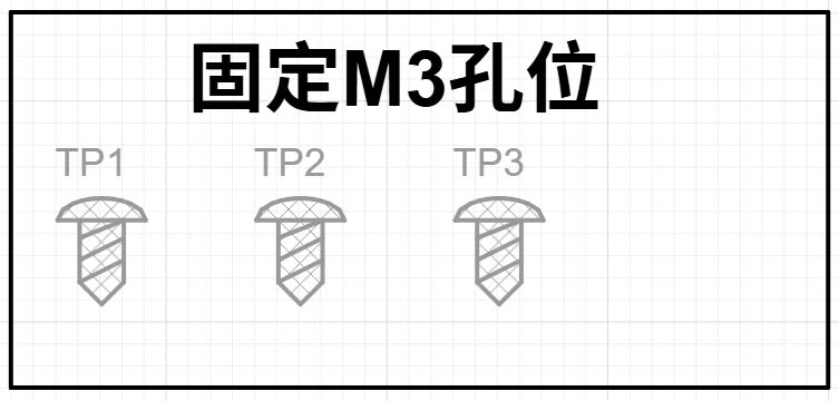
| M3 Fixing Hole | 3 pieces | Mechanical Fixing | Easy to install on the housing or structural component |
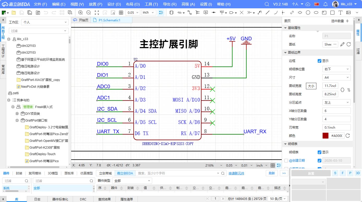
4. Pin Assignment
The XIAO series development boards are small in size, but their commonly used interfaces are relatively complete. During the design process, I prioritized bringing out the commonly used communication interfaces rather than making complex connections for all GPIOs. This approach can reduce the difficulty of wiring and also keep the board clear.
| Interface / Signal | Connected Object | Usage |
|---|---|---|
| 5V / VCC | Grove Interface, Power Input Module | Power the external module |
| GND | All interfaces are grounded together | Establish a unified reference level |
| SDA | Grove I2C Interface | I2C Data Line |
| SCL | Grove I2C Interface | I2C Clock Line |
| TX | Grove UART Interface | Serial Port Transmission |
| RX | Grove UART Interface | Serial Port Reception |
| VBAT / External Input | Power switch, power network | External power supply input |
During pin planning, I paid special attention to the requirement that GND must be common. Whether it is a sensor, display, or external power supply, as long as it communicates signals with XIAO, it must have a common GND reference; otherwise, the signal level will be unstable, and communication may fail.
5. Schematic Design Process
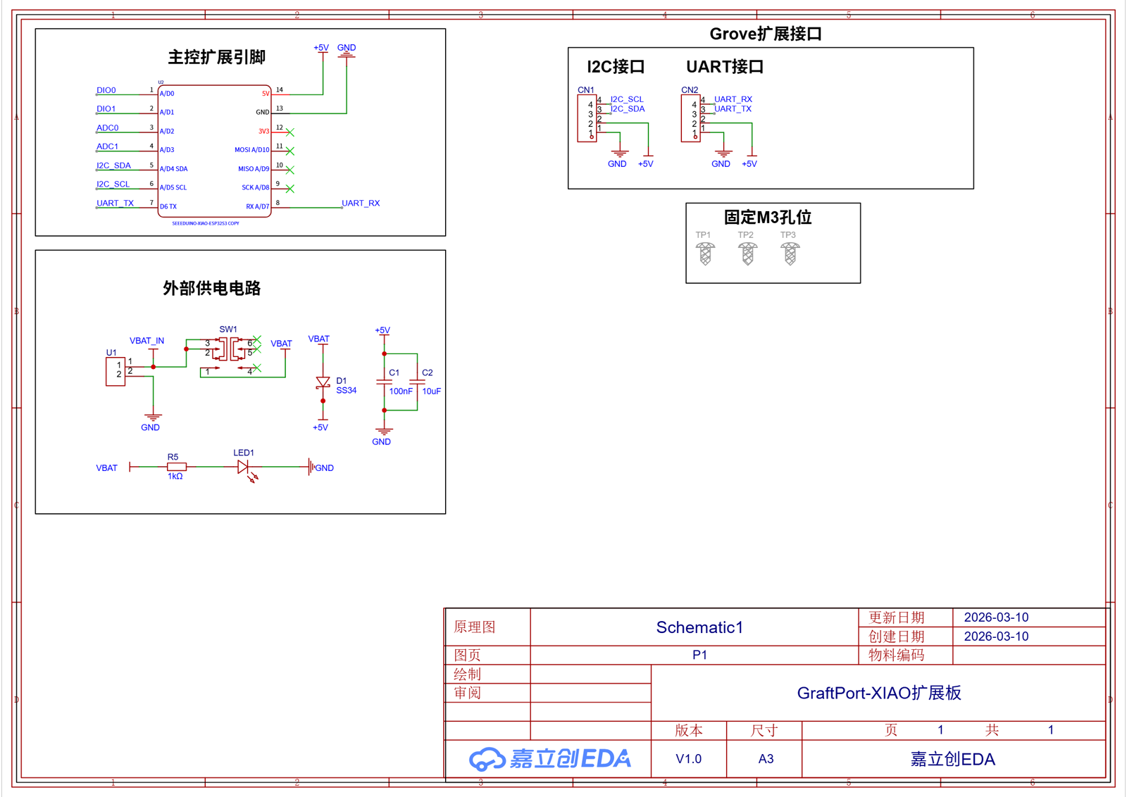
The schematic diagram is the first step in PCB design, expressing the logical relationships of the circuit. My schematic diagram is drawn using modularization, mainly divided into four parts: the main control module, the Grove interface module, the power supply module, and the mechanical fixing module.
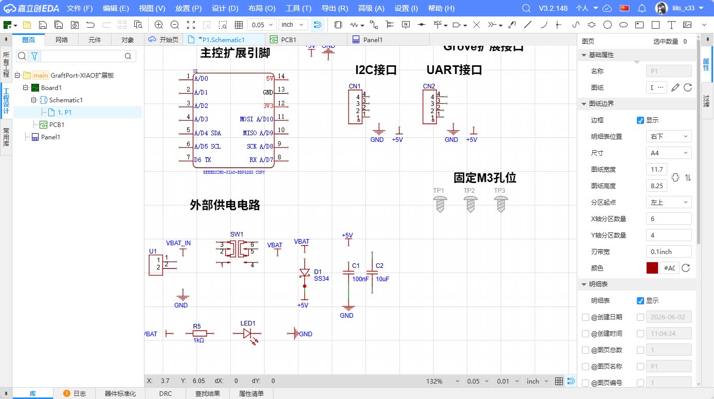
5.1 Create a Project and Place Components
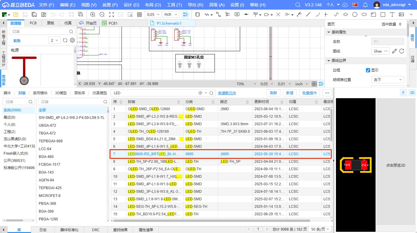
I first create a new project in JLCEDA, then create a schematic file. Next, I search for and place the required components from the component library, including the XIAO microcontroller, Grove interface, power switch, LED, resistor, capacitor, and mounting holes.
When placing components, I didn't rush to connect wires right away. Instead, I first arranged them according to functional modules: XIAO was placed in the center of the schematic, Grove interfaces on one side, and power input, power switch, and LED on the other side. The advantage of doing this is that it is easier to understand the signal flow when checking the schematic later.
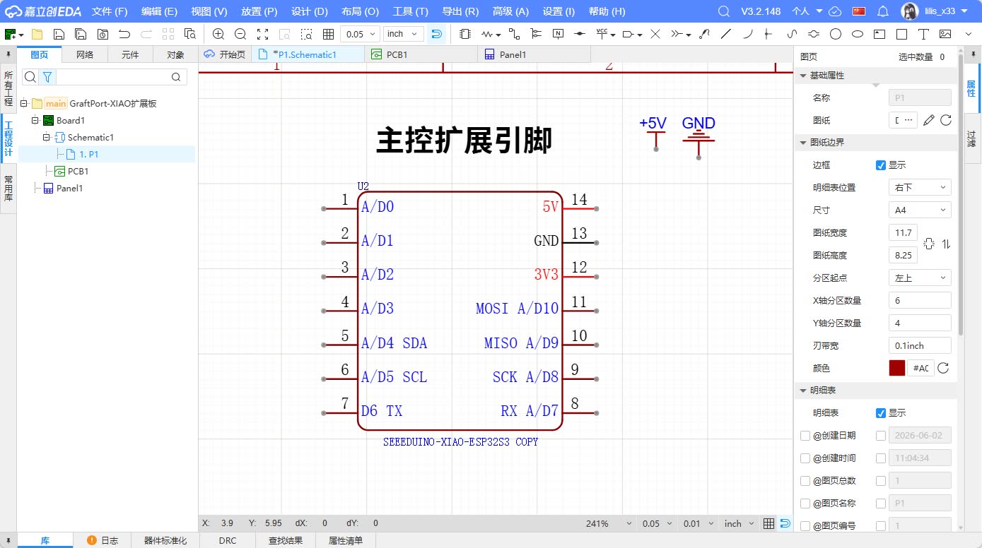
5.2 Main Control Module
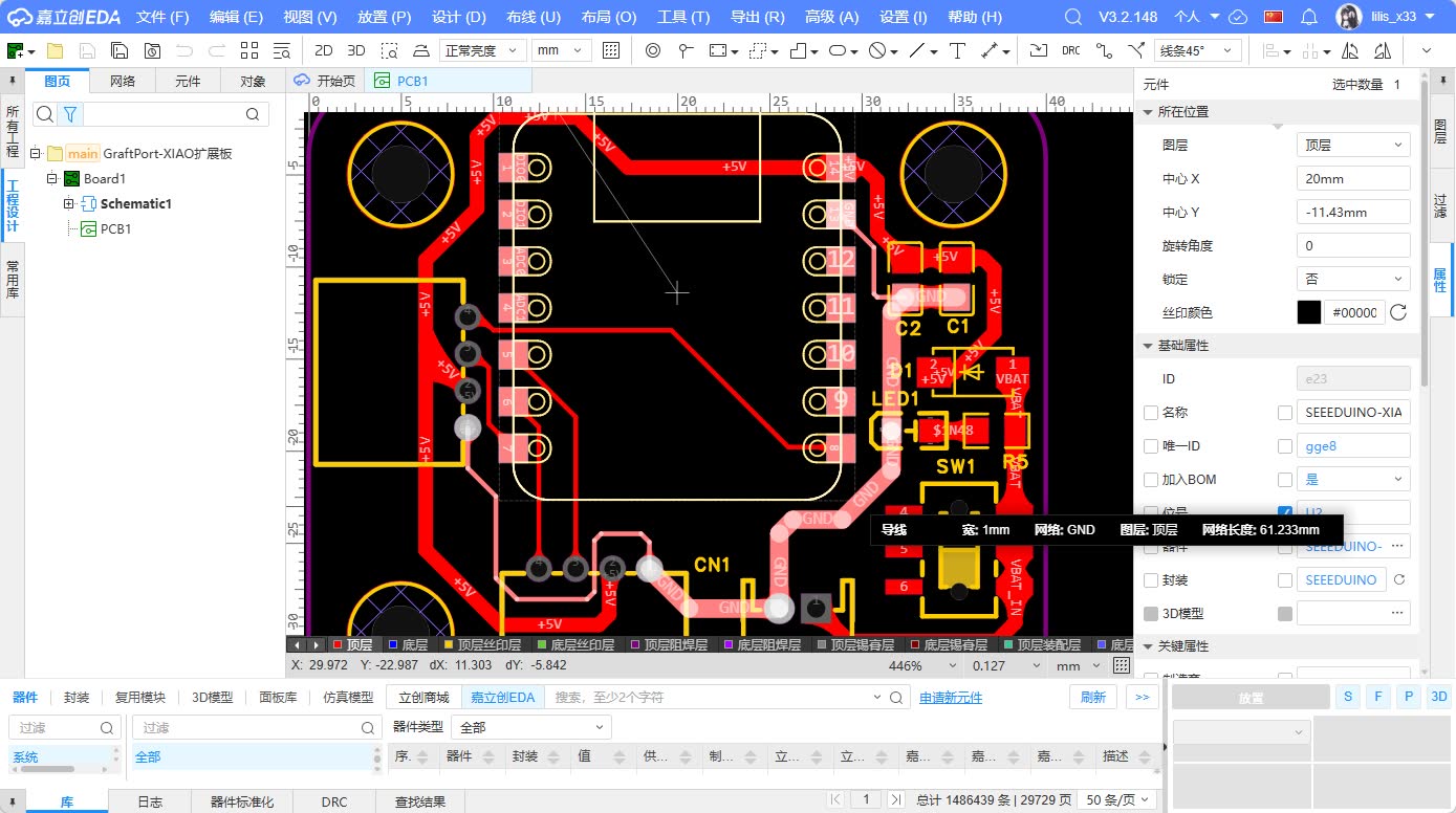
The core of the main control module is the Seeed Studio XIAO series development board. In the schematic diagram, I focused on confirming whether the power pins, GND pins, I2C pins, and UART pins of the XIAO are correctly connected to the corresponding networks.
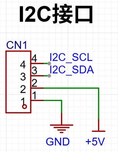
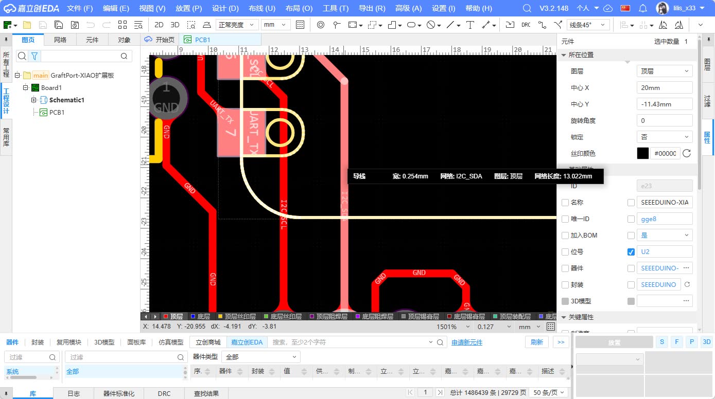
5.3 Grove I2C Interface
The I2C interface is used to connect sensors or displays. The advantage of I2C is that it only requires two signal lines, SDA and SCL, to connect multiple devices. Many common modules support I2C, such as OLED displays, LCD displays, temperature and humidity sensors, and light sensors.
In the schematic diagram, the Grove I2C interface includes four pins:
- VCC: Supplies power to external modules.
- GND: Common ground with the main controller.
- SDA: I2C data line.
- SCL: I2C clock line.
Here, I specifically note that the naming of SDA and SCL should be consistent with that of the XIAO master control end. Using network labels can reduce long-line crossovers and make the schematic clearer.
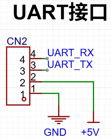
5.4 Grove UART Interface
The UART interface is used for point-to-point serial communication and can be connected to serial screens, GPS modules, or other serial devices. UART typically includes four pins: TX, RX, VCC, and GND.
When designing the UART interface, one issue to note is the direction of TX and RX . The TX of the main controller needs to be connected to the RX of the external device, and the RX of the main controller needs to be connected to the TX of the external device. To make subsequent wiring clearer, I have tried to retain the TX/RX markings in both the schematic diagram and PCB silkscreen.
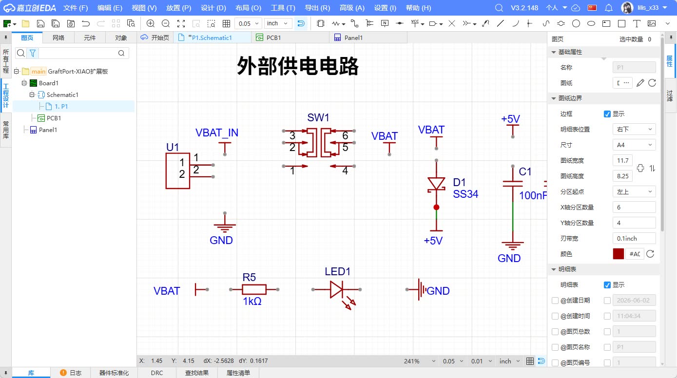
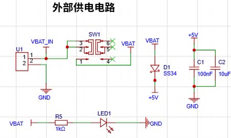
5.5 External Power Supply, Power Switch, and Indicator Lights
To enable the expansion board to operate independently without being connected to a computer's USB, I added an external power supply module. This module includes an external power input, a power switch, a filter capacitor, and a power indicator.
The power path is roughly as follows: External power enters through the VBAT / power interface, passes through the power switch SW1, and then enters the VCC network of the board. When the switch is turned on, power is supplied to the XIAO and Grove interfaces, while also lighting up LED1.
LED1 is the simplest output device on this board. It is connected to the power network through current-limiting resistor R5, and its function is to indicate whether the board has been powered on. This small feature is very useful during debugging because as long as the LED lights up when the switch is turned on, it can be initially determined that the power input and switch path are normal.
Filter capacitors C1 and C2 are placed on the power supply network to reduce power supply fluctuations. Although the functions of this board are not complex, adding capacitors can make the power supply more stable, especially when sensors or displays are subsequently connected.
5.6 Fixing Holes
I added 3 M3 mounting holes in the schematic and PCB. The mounting holes do not participate in electrical connections, but they are very important for the actual project. If this board needs to be installed into the enclosure, bracket, or final project structure in the future, the mounting holes can make the circuit board installation more stable.
5.7 Schematic Diagram Inspection
After completing the schematic diagram, I conducted a basic inspection. The key points of the inspection included:
| Inspection Items | Inspection Content |
|---|---|
| Power Connection | Is VCC / 5V connected to the interface that requires power supply? |
| GND connection | Are all modules grounded together? |
| Network Naming | Are the names of SDA, SCL, TX, and RX consistent? |
| LED Polarity | Is the positive and negative direction of the LED correct? |
| Resistance Position | Whether the LED is connected in series with a current-limiting resistor |
| Encapsulation Match | Has the schematic component been assigned the correct PCB footprint? |
| Unconnected Pin | Are there any critical pins that should not be left floating? |
This step is crucial because if the network connections in the schematic are incorrect, no matter how beautiful the subsequent PCB routing is, it will be meaningless.
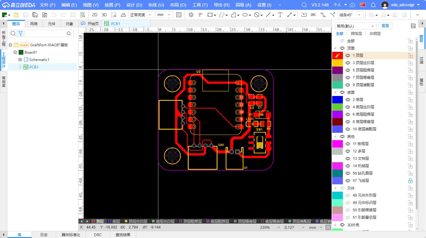
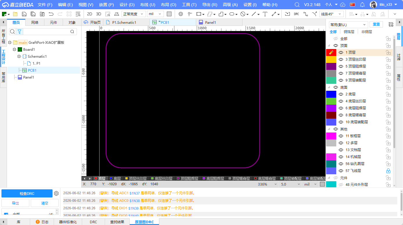
6. Convert from schematic to PCB
After completing the schematic check, I transferred the design to the PCB.
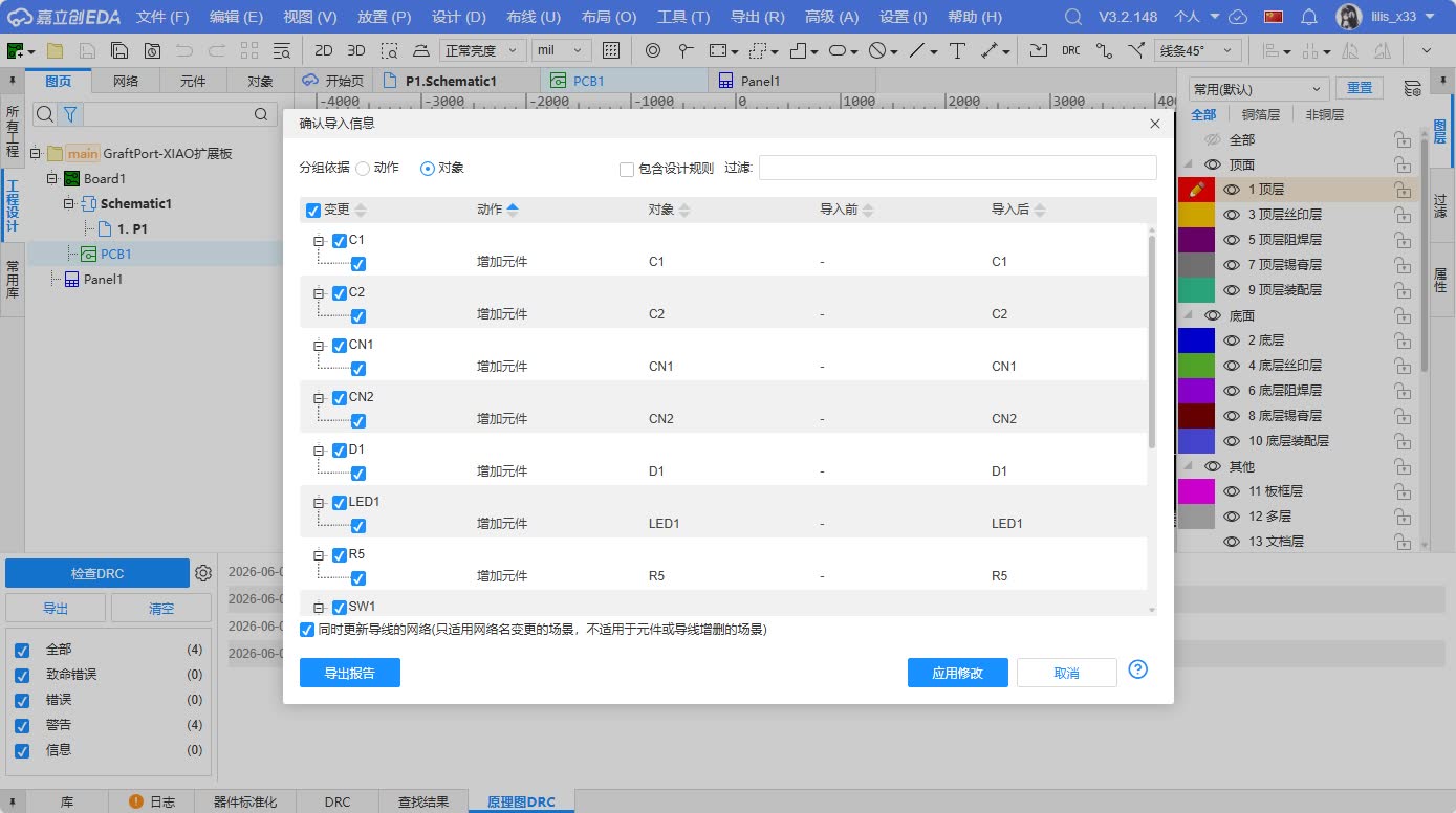
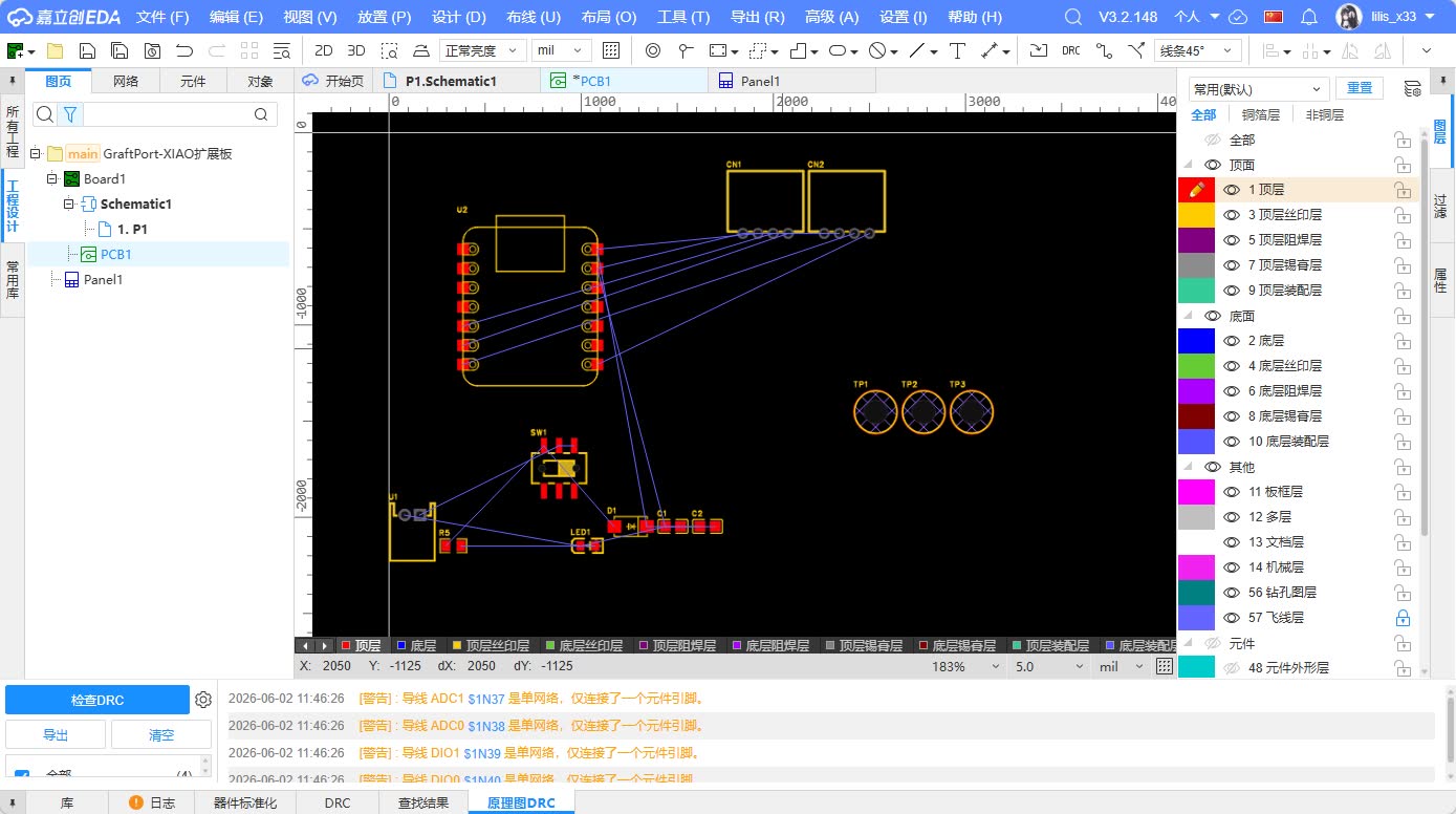
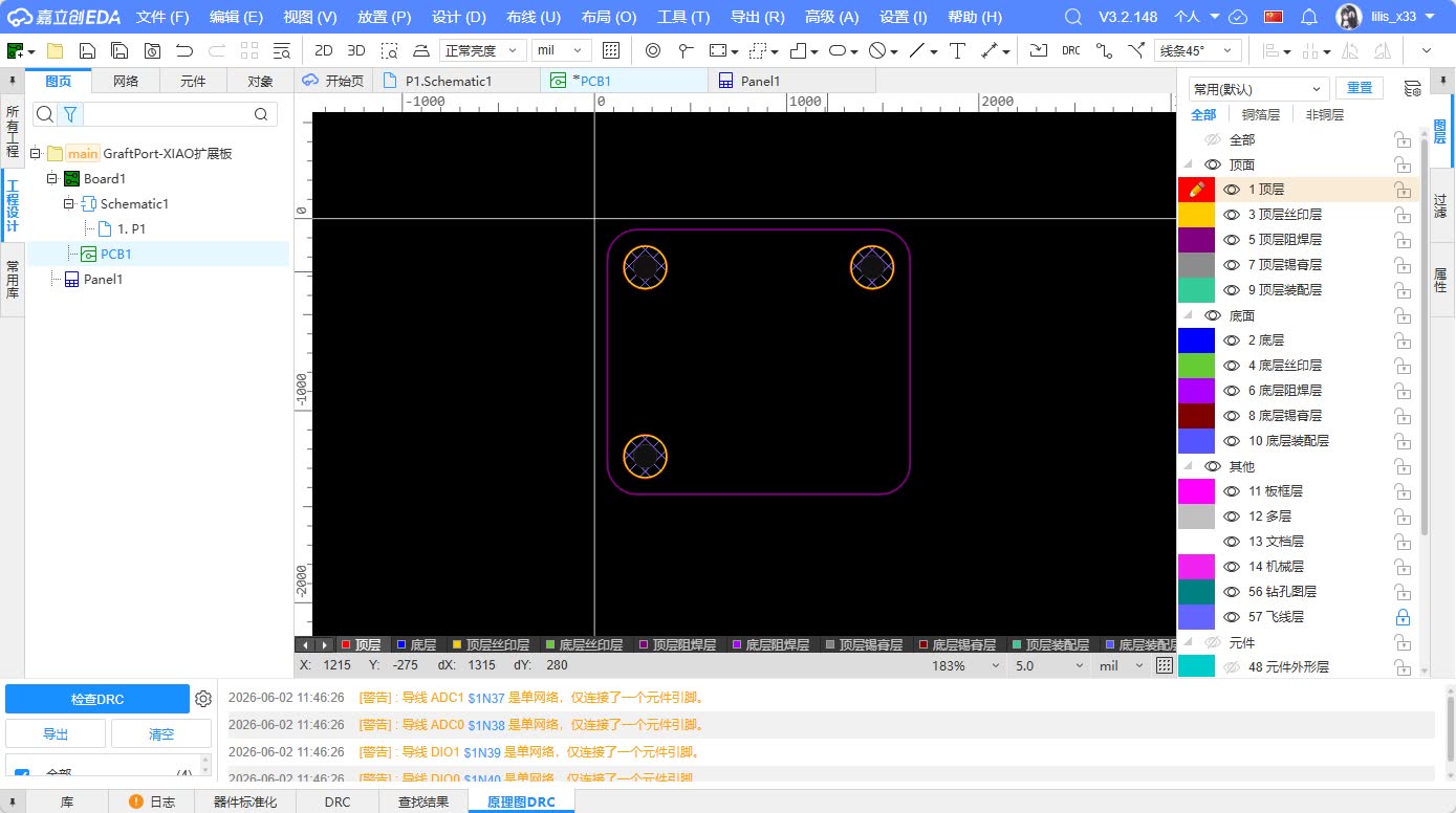
This step will import the component packages from the schematic into the PCB page while preserving the connection relationships between each network. When first entering the PCB page, all components are usually stacked together, and many ratsnest lines can be seen. Ratsnest lines represent the networks that should be connected in the schematic but have not yet been physically routed on the PCB.
At this stage, I mainly did three things:
- Confirm that all components have been successfully imported into the PCB.
- Check if each component package looks reasonable.
- Rearrange the positions of components according to the actual usage method.
If the package dimensions are incorrect, such as the hole spacing of the Grove interface not matching, even if the board is fabricated later, real components cannot be soldered. Therefore, I check the package outline, the number of pads, and their orientation before layout.
7. PCB Layout Process
PCB layout determines the position of components on a real circuit board. My layout approach is to first determine the form factor and interfaces, then arrange the main controller, and finally handle the power supply and auxiliary components.
7.1 Plate and Frame Design
I first draw the PCB outline to keep the board at a size suitable for handheld use and installation. The board frame should not be too small, otherwise the interfaces and mounting holes will be crowded; nor should it be too large, otherwise it will be unfavorable for subsequent installation and material saving.
Place the fixing holes at the edge of the board, avoiding the main routing area as much as possible. This way, when using screws for fixing later, it is less likely to touch the pads or traces.
7.2 Master Control Location
The XIAO main control board is placed in the middle area of the PCB. This approach has two advantages: first, the routing paths from the XIAO to each interface are relatively short; second, it is more convenient for subsequent plugging and unplugging of the USB cable or replacement of the main control board.
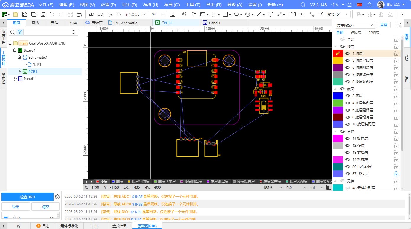
I also need to consider the orientation of XIAO's USB port to avoid it being blocked by other components. If the USB port is blocked, subsequent programming and debugging will be very troublesome.
7.3 Interface Location
Grove interfaces are placed at the edge of the board because they need to connect external cables. If the interfaces were placed in the middle of the board, cable insertion would conflict with other components, and it would also be inconvenient to organize the cables.
The I2C and UART interfaces should be placed separately as much as possible, and the interface types should be clearly marked on the silkscreen. This can reduce the possibility of plugging into the wrong interface during subsequent use.
7.4 Power Module Location
The power input and power switch are placed in relatively independent positions. My idea is to keep the power path as short and clear as possible: the power input first goes to the switch, then to the power network and indicator light. The LED is placed in an easily observable position to facilitate quick status judgment during power-on testing.
The filter capacitor should be placed as close as possible to the power input or power supply network, so that it can stabilize the voltage more effectively.
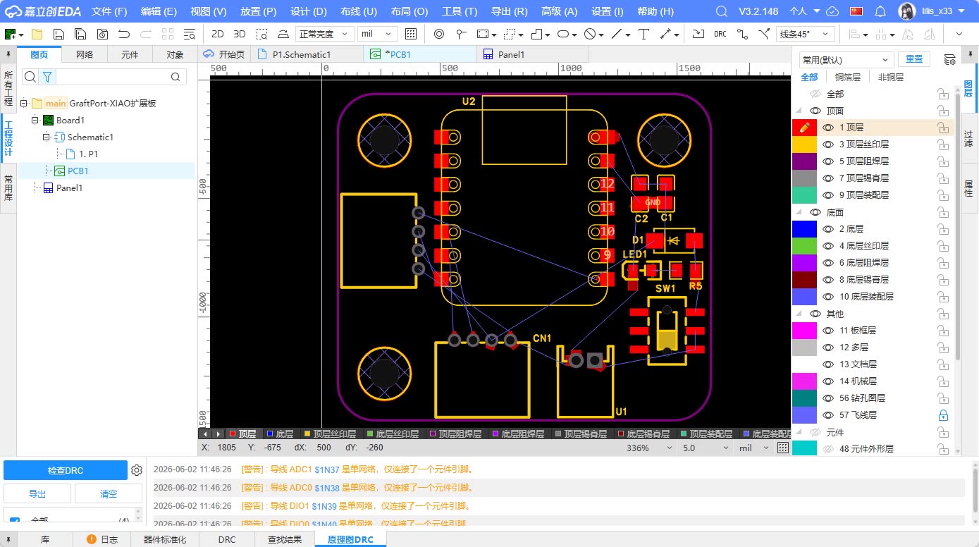
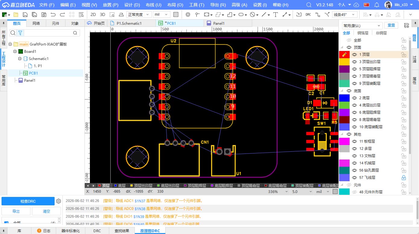
8. PCB Wiring Process
This PCB uses a relatively simple single-layer wiring concept. Since the main function of this board is interface expansion and it does not involve high-speed signals, I prioritize clear, reliable, and easily inspectable traces.
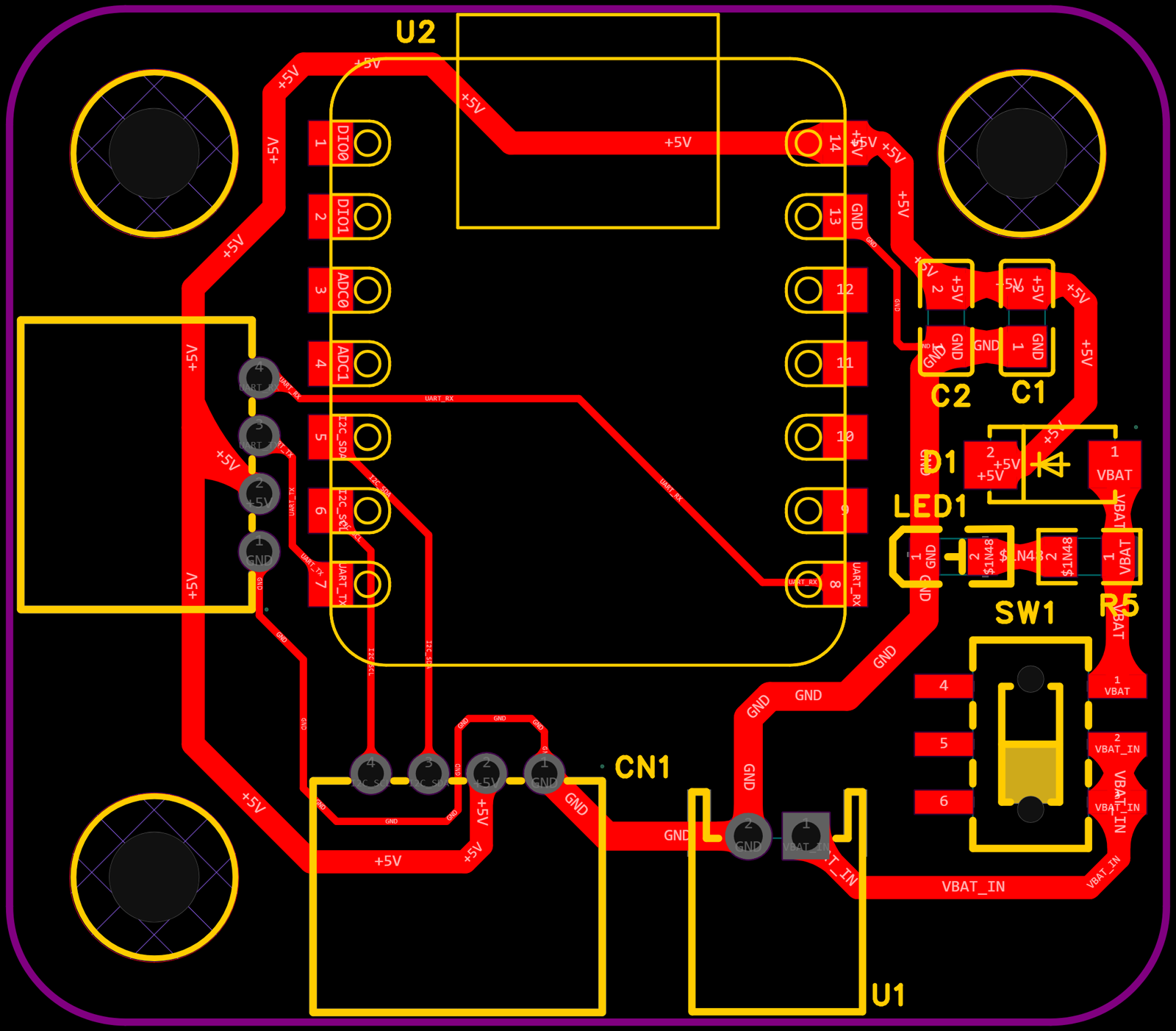
When wiring, I followed the following principles:
- Power lines and GND lines should be as wide as possible compared to ordinary signal lines.
- Keep the traces as short as possible to reduce unnecessary detours.
- Try to avoid sharp turns and use 45° corners to make the route smoother.
- The SDA / SCL of I2C should be as parallel as possible, with clear paths, and not mixed with the power switch area.
- The TX/RX of the UART maintains clear direction, facilitating subsequent debugging.
- Reserve space around the fixing holes to avoid conflicts between screws and wiring.
Since large-area copper pouring was not done, I specifically checked whether the GND network was complete. All Grove interfaces, XIAO main controller, power input, and LED must be connected to the same GND network. If the GND is disconnected, the circuit may appear to be correctly connected, but the actual communication will be unstable.
8.1 Power Supply and GND
Power and GND are the most fundamental and error-prone parts of a PCB. My power line is externally input, passes through a switch, and then is distributed to the XIAO and Grove interfaces. GND serves as the common reference for all modules.
During the inspection, I focused on confirming:
- Is the external power supply GND connected to XIAO GND?
- Is the Grove interface GND connected to the main control GND?
- Is the LED circuit complete?
- Whether the power supply is disconnected when the switch is turned off.
8.2 Communication Line
Both I2C and UART belong to low-speed communication lines, but still need to maintain clear connections. I2C uses two lines, SDA and SCL, while UART uses two lines, TX and RX.
On the PCB, I try to ensure that these signal lines do not cross the power switch and LED areas, reducing crossovers and misreads. For subsequent debugging, a clear routing path is more important than a complex layout.
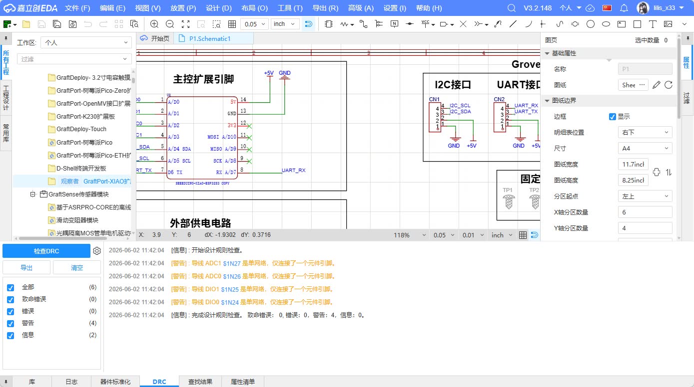
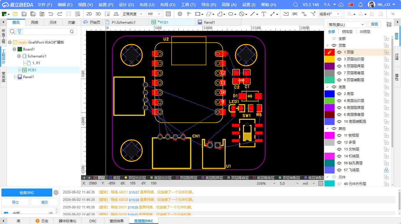
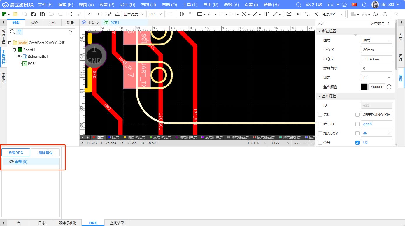
9. Design Rule Check and Modification
After completing the PCB routing, I performed a Design Rule Check (DRC). DRC can help identify issues such as too close trace spacing, unconnected nets, pad conflicts, and board outline errors.
My key inspection points include:
| Inspection Items | Inspection Purpose |
|---|---|
| Unrouted / Unwired | Confirm that all flying wires have been connected |
| Clearance / Spacing | Avoid short circuits caused by the distance between traces and pads being too close |
| Width / Line Width | Confirm that the widths of the power and signal lines are reasonable |
| Hole / Hole Position | Confirm that the fixing holes and component pads do not conflict |
| Silkscreen / Screen Printing | Confirm that the text does not cover the pads and the interface label is readable |
| Board outline / Board frame | Confirm that the board shape is closed and can be produced normally |
If an error occurs during the inspection, I will return to the PCB page to make modifications. For example, moving components, adjusting routing paths, increasing line spacing, or modifying silkscreen positions. This process has made me realize that PCB design is not completed in one go but requires continuous cycling between "layout, routing, inspection, and modification".
10. 3D Preview and Hero Shot
After completing the PCB, I used the 3D preview function of the software to view the overall effect of the board. The 3D preview can help identify some issues that are not obvious in the 2D view, such as interface orientation, component height, main control board position, and fixing hole distribution.
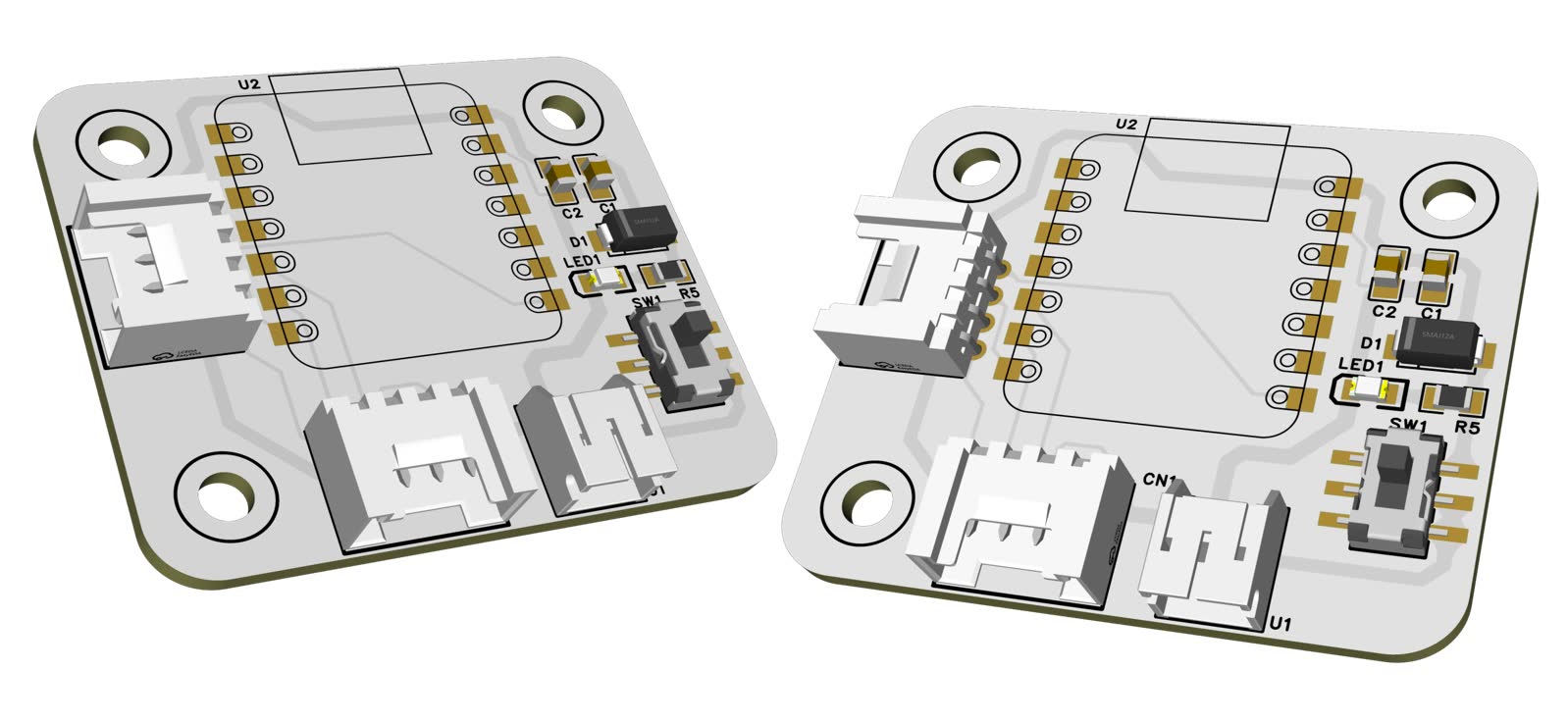
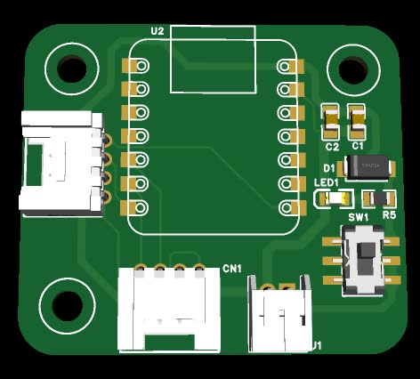
As can be seen from the 3D renderings, the XIAO main controller is located in the middle of the board, with Grove interfaces, power switches, and power indicators distributed around the main controller. The overall structure is relatively compact, with all interfaces facing the board edge, making it suitable as an expansion baseboard for small sensors or interactive devices.
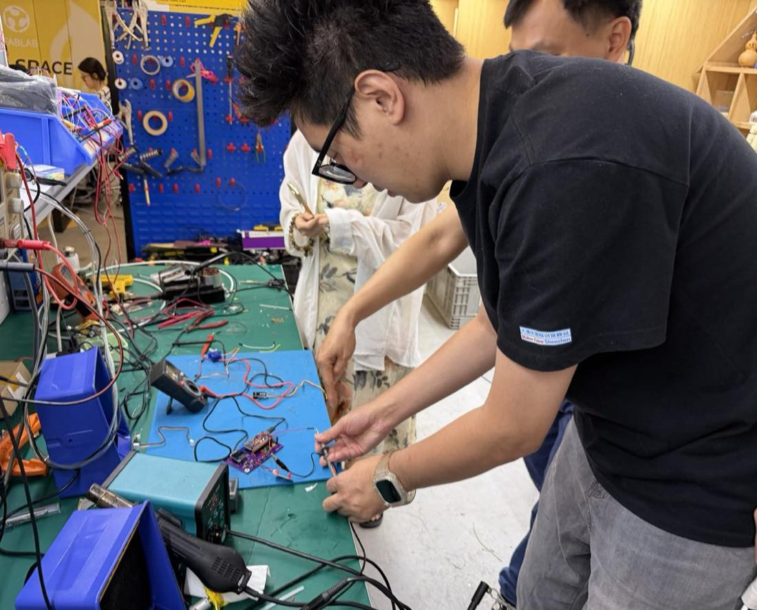
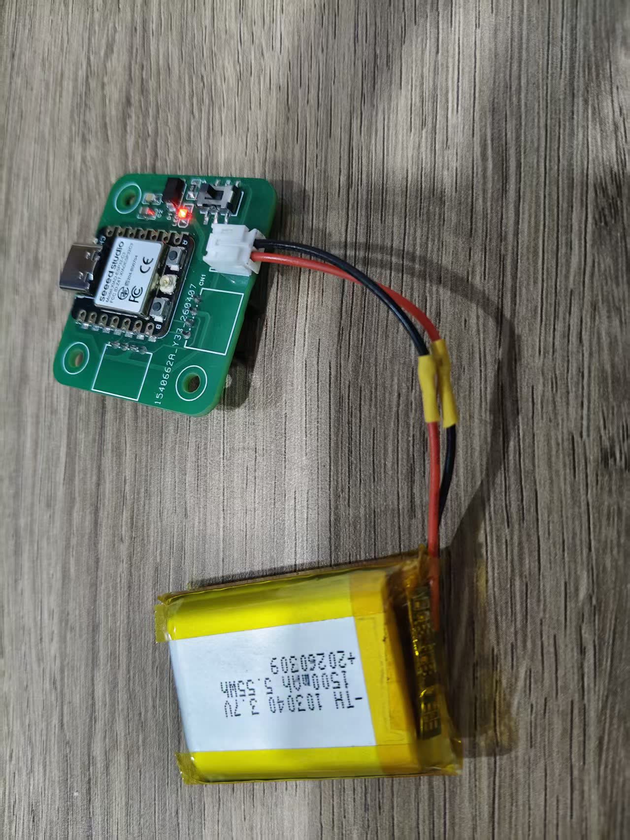
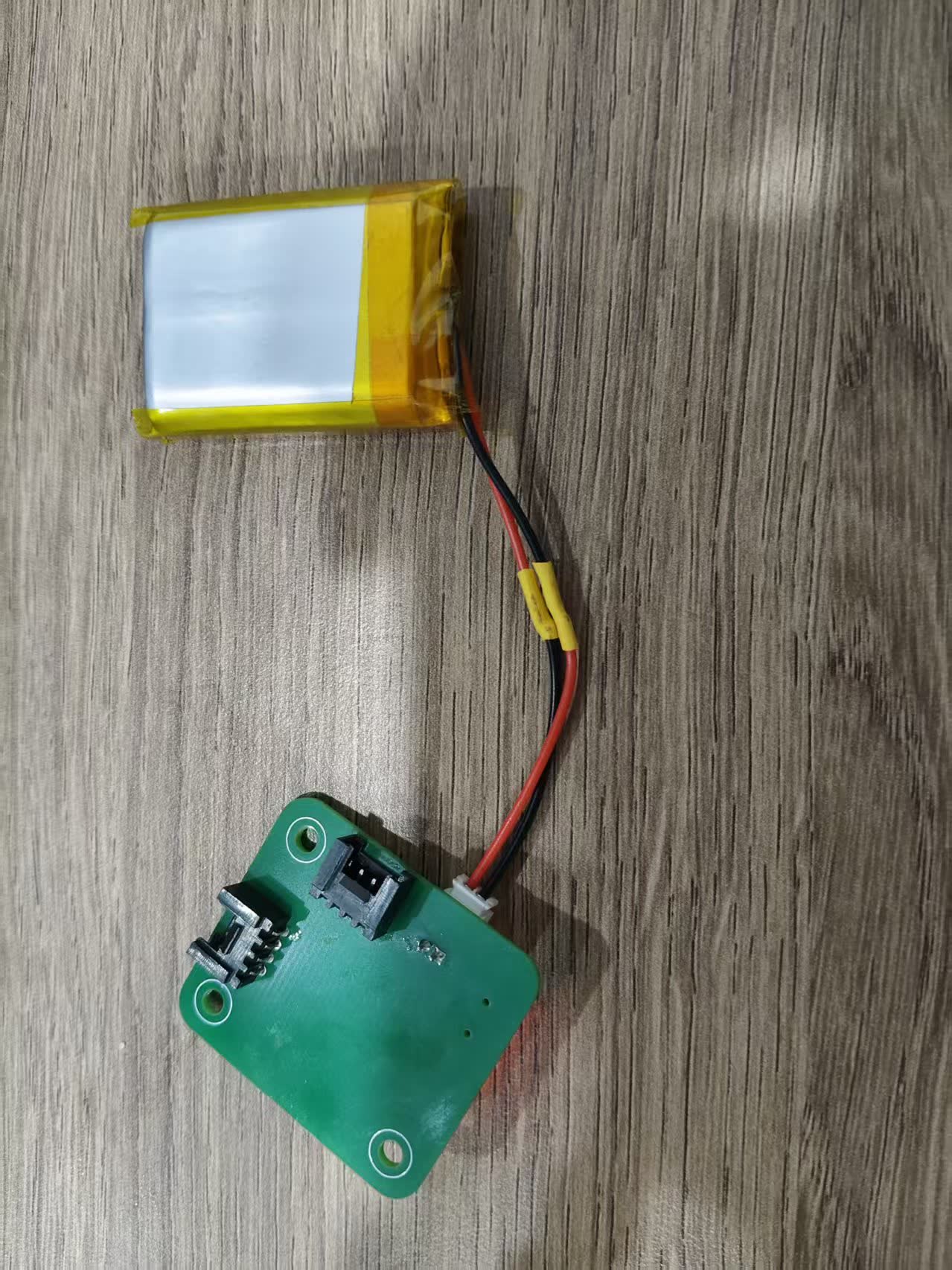
In addition to 3D screenshots, I also took photos of the external polymer battery LED lighting up after the welding was completed.
As can be seen from the figure, the XIAO main control board is located in the middle area, with Grove interfaces, power switches, and indicator lights distributed around the main control. The overall structure is relatively compact, making it suitable as an expansion baseboard for small sensors or interactive devices.
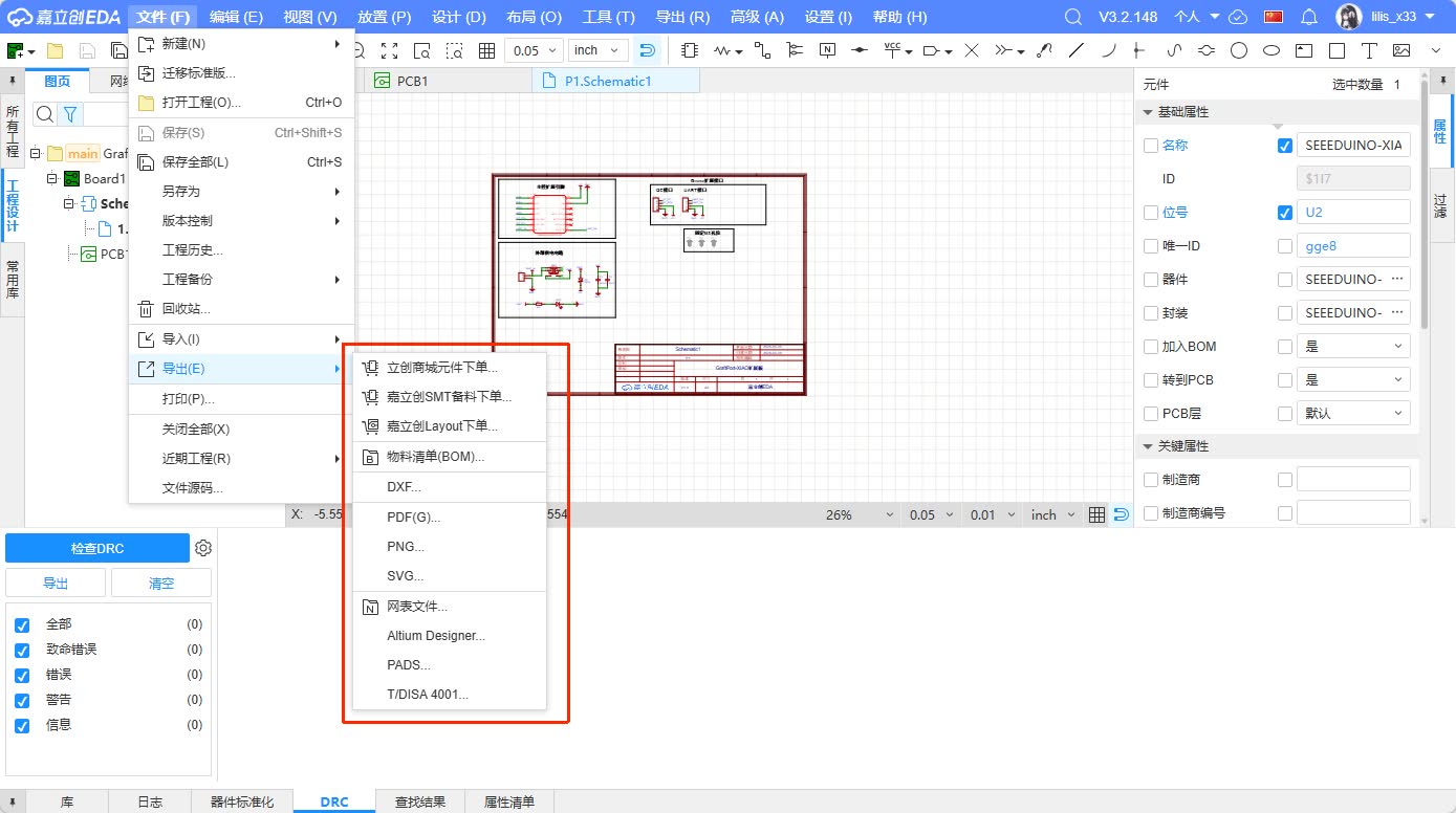
11. Export design files
After the design is completed, I need to upload the source files to my personal webpage as an attachment for this week's assignment. The main file for this time is the EasyEDA project file:
ProPrj_GraftPort-XIAO扩展板_2026-03-14.epro2
If the subsequent process enters the board manufacturing stage, the following files can still be exported:
- Gerber files: Used for PCB production.
- Drill file: Used for drilling.
- BOM File: Used for component list.
- Pick and Place File: Used for SMT positioning.
- Schematic PDF: Used for display and inspection.
12. Summary of This Design
Through this week's assignment, I experienced for the first time a relatively complete process from circuit requirements to PCB design files. Compared with directly connecting using breadboards or DuPont wires, PCB design requires considering more practical issues in advance, such as component packages, interface orientation, routing paths, power supply stability, mounting hole positions, and subsequent testing methods.
The functionality of this GraftPort-XIAO expansion board is not complex, but it contains the basic elements required for a complete development board: controller interface, input interface, output indication, power control, and communication interface. It can continue to be used as a basic expansion board for subsequent input devices, output devices, and final projects.
My biggest takeaway this time is understanding that a correct schematic does not necessarily mean the PCB will be usable . A schematic addresses electrical connection issues, while a PCB also has to address issues such as position, orientation, size, soldering, and testing in the real world. In future circuit board designs, I will check package dimensions and interface orientation earlier and reserve more space for testing and installation during the PCB layout phase.