Week 8 - Electronics Production (Individual Assignment)
Assignment Goal
- Individual assignment: Make and test a microcontroller development board.
Files
Overview
This week I produced the PCB I designed back in Week 6. The full journey went: trying the JLCPCB board first, spotting a few problems, fixing the design in KiCad, milling my own board on the lab's CNC machine, soldering with solder paste and a constant temperature heating station, and finally testing and programming it. It had more plot twists than expected, but everything worked in the end! Cheers~
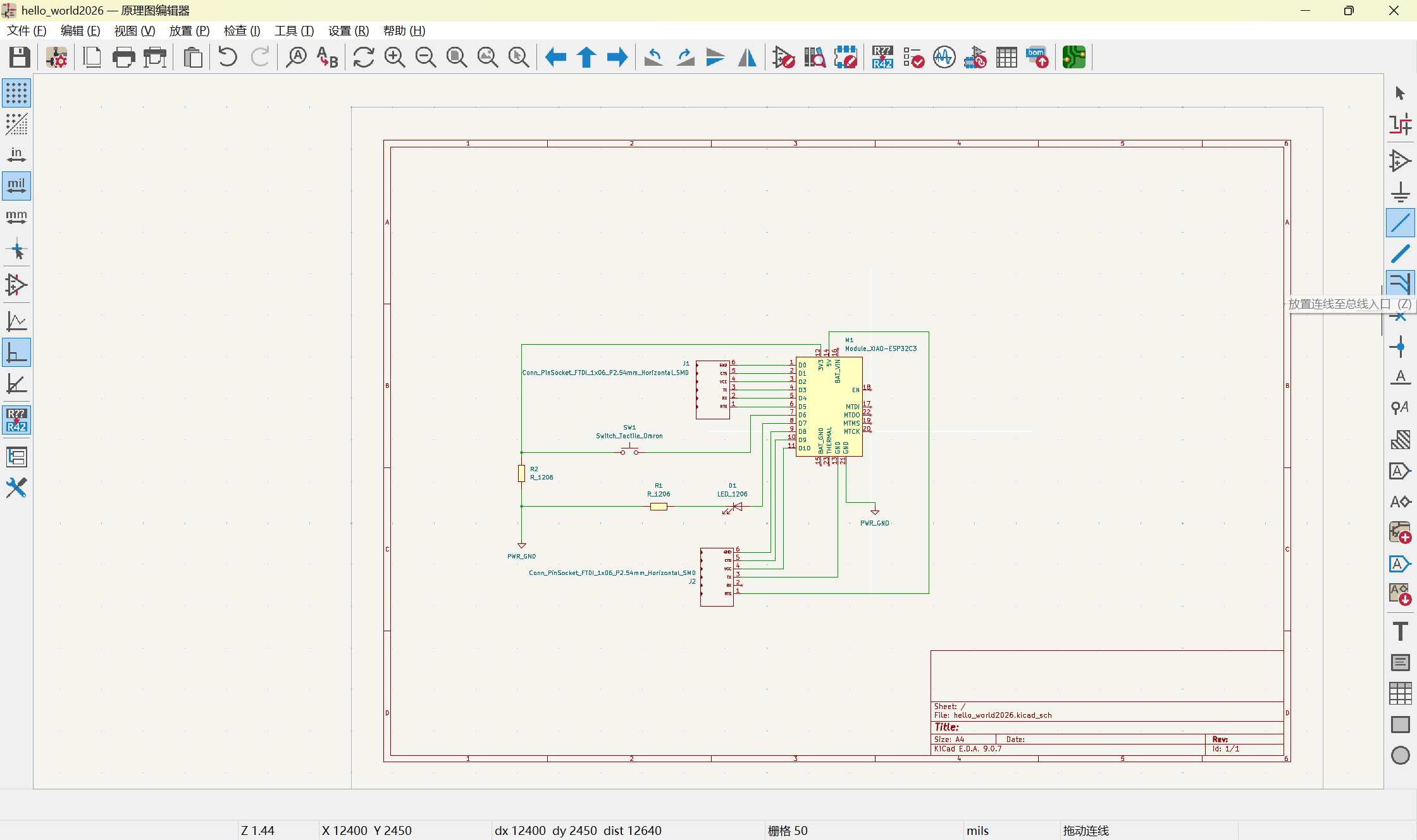
Part 1: First Try Assembling the JLC Board
When the JLCPCB boards arrived (covered in the group assignment), I couldn't wait to try soldering. I assembled resistors, an LED, a tactile switch, a socket, and the XIAO ESP32C3 onto the board.
The socket and XIAO powered up fine. But the LED and button weren't cooperating. After some head-scratching, I traced it back to a few likely culprits:
- The LED was probably soldered in the wrong direction, the cathode and anode marking on 1206 packages is easy to misread.
- The resistors I used were not 1206 spec, I grabbed what was nearby without double-checking the volume.
- The switch might have been installed in the wrong orientation too.
The temperature and humidity sensor test worked fine though, which confirmed the basic MCU connection was good. So rather than rework the JLC board immediately, I decided to fix the root issues in the design and cut my own PCB properly.
Part 2: Fixing the Design in KiCad
Before milling, I went back to KiCad and found two problems that needed fixing.
Missing ground line: The schematic was missing one ground connection entirely. I added the missing wire and re-ran DRC to confirm no errors.
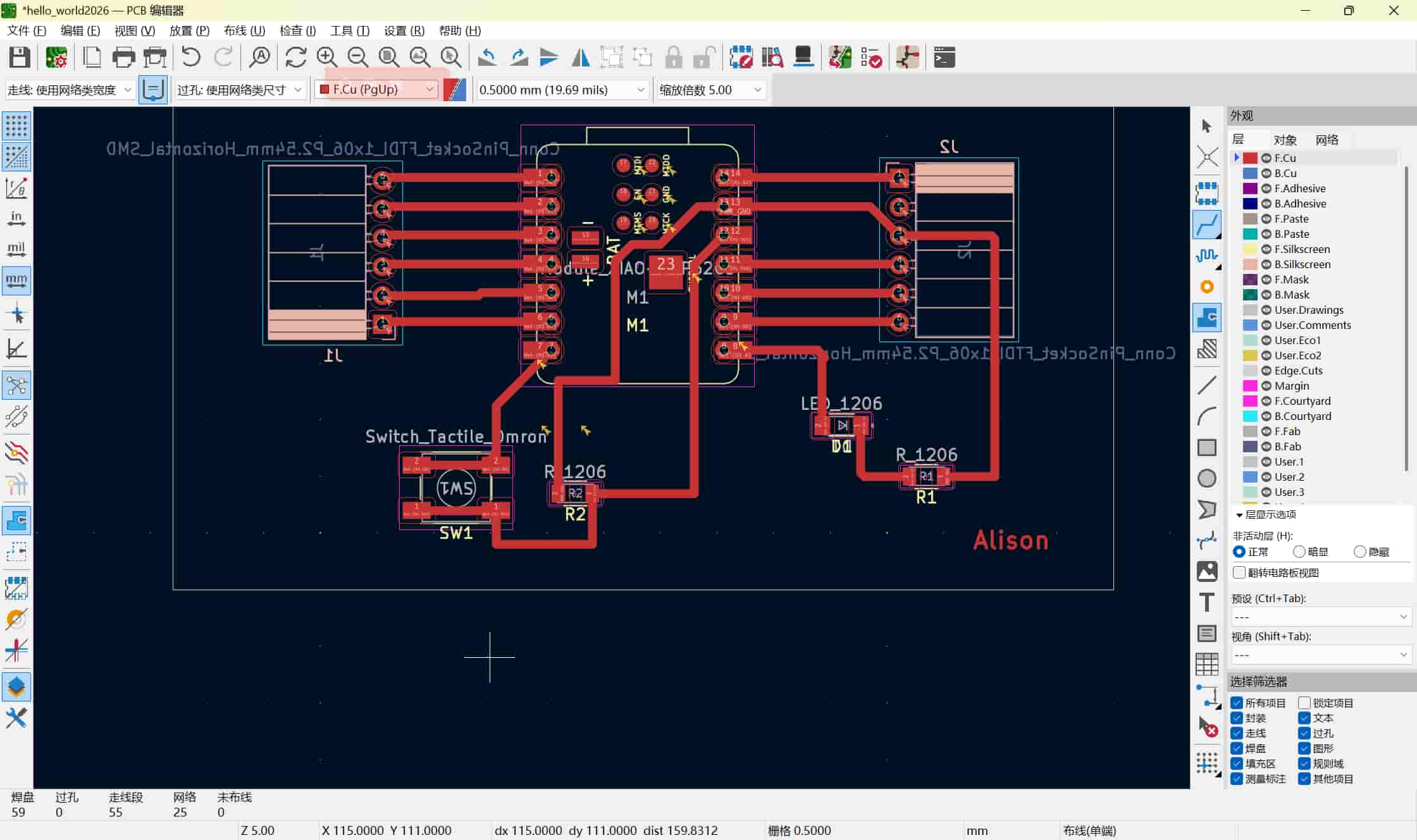
Traces too thin: My instructor pointed out the traces were too narrow, they had a higher chance of breaking during milling. I updated the trace width from 0.5 mm to 0.8 mm, which made a noticeable visual difference and gave the milling bit a safer margin.
After making both corrections, I re-exported the Gerber files.
Part 3: From Gerber to G-Code
The CNC machine doesn't read Gerber files directly, so there's a conversion chain:
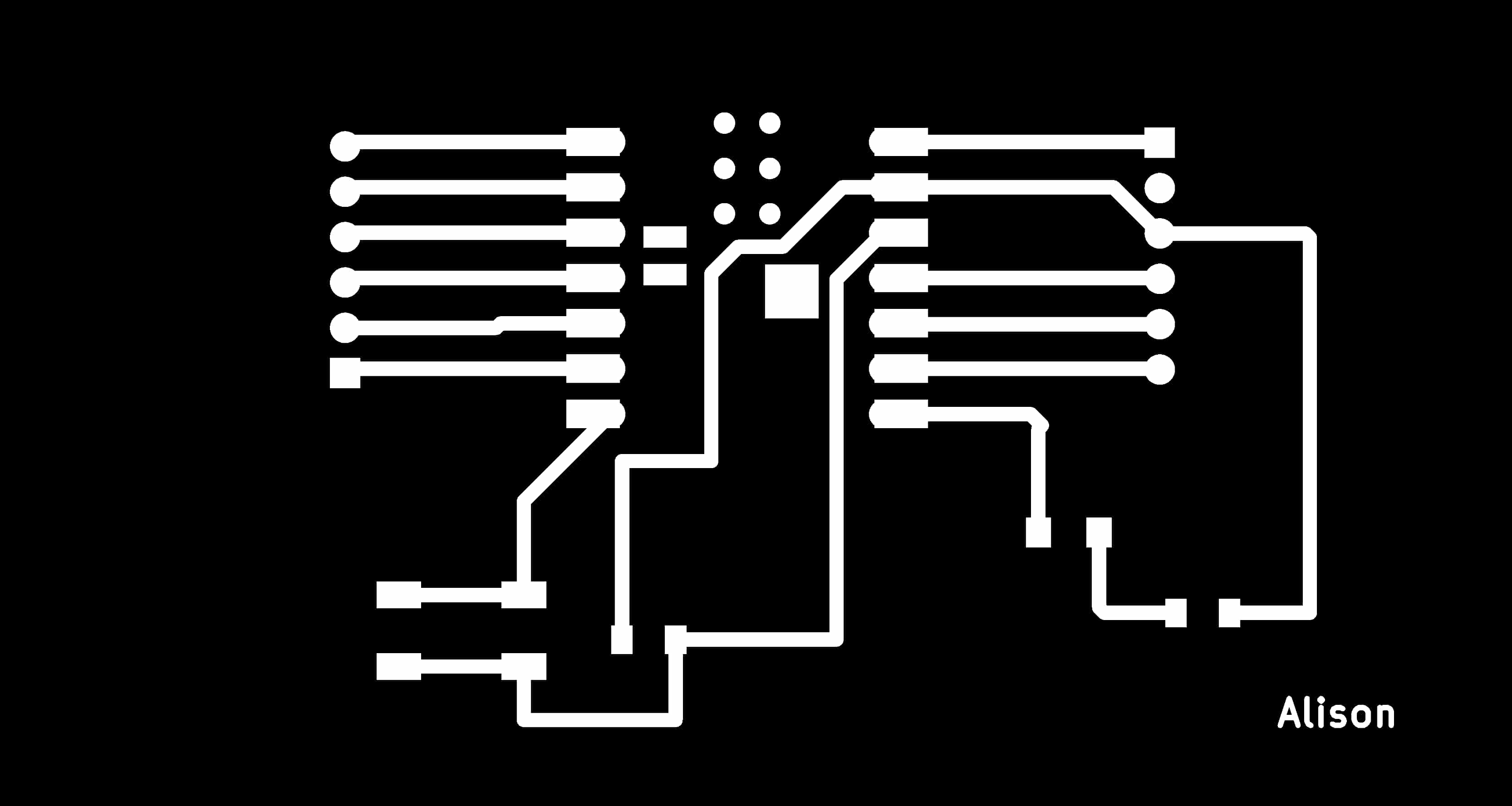
- Export Gerber files from KiCad → two files: the copper trace layer and the board outline.
- Convert Gerber → PNG using an online tool. This produces two PNG images: one for the internal traces, one for the outer edge.

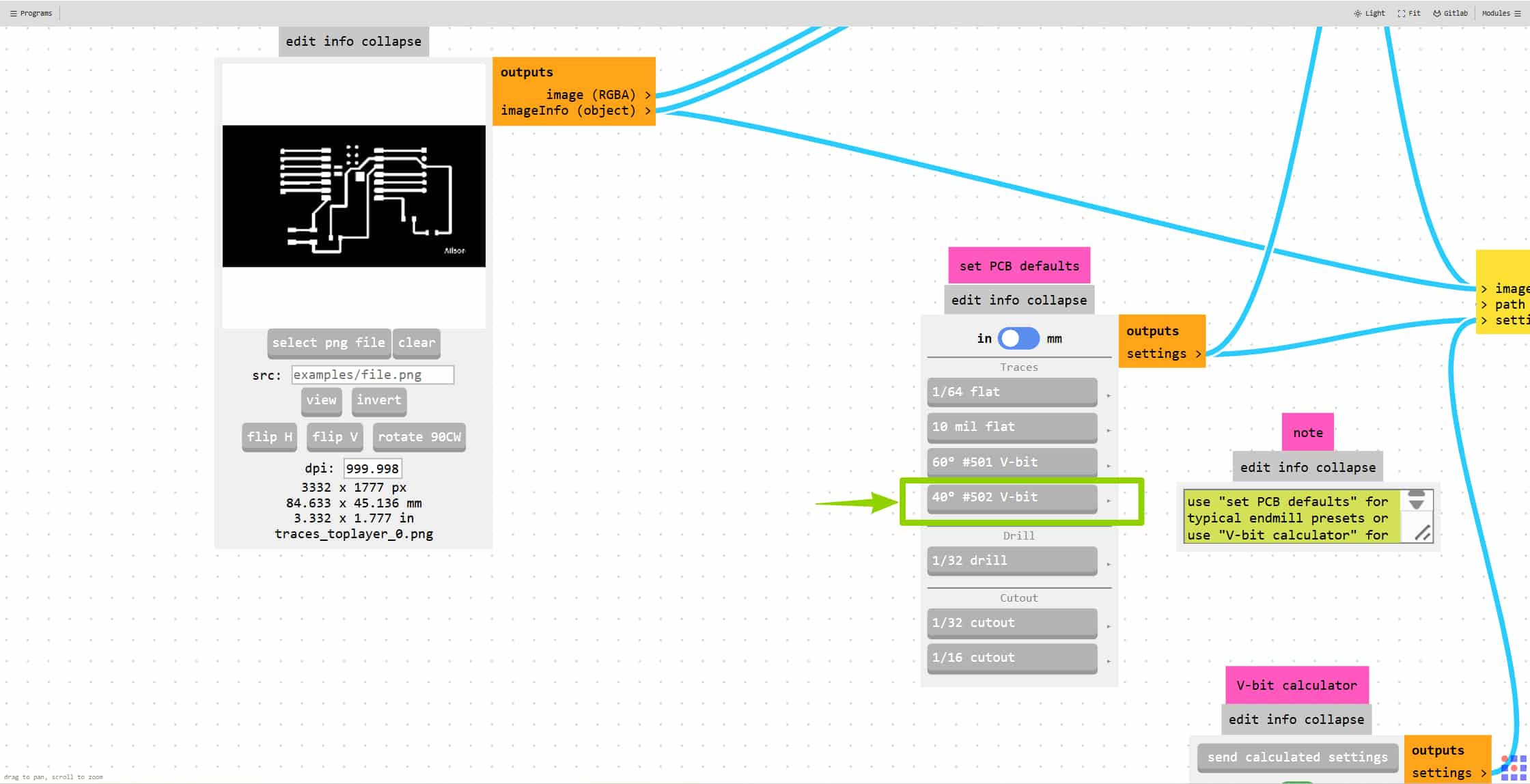
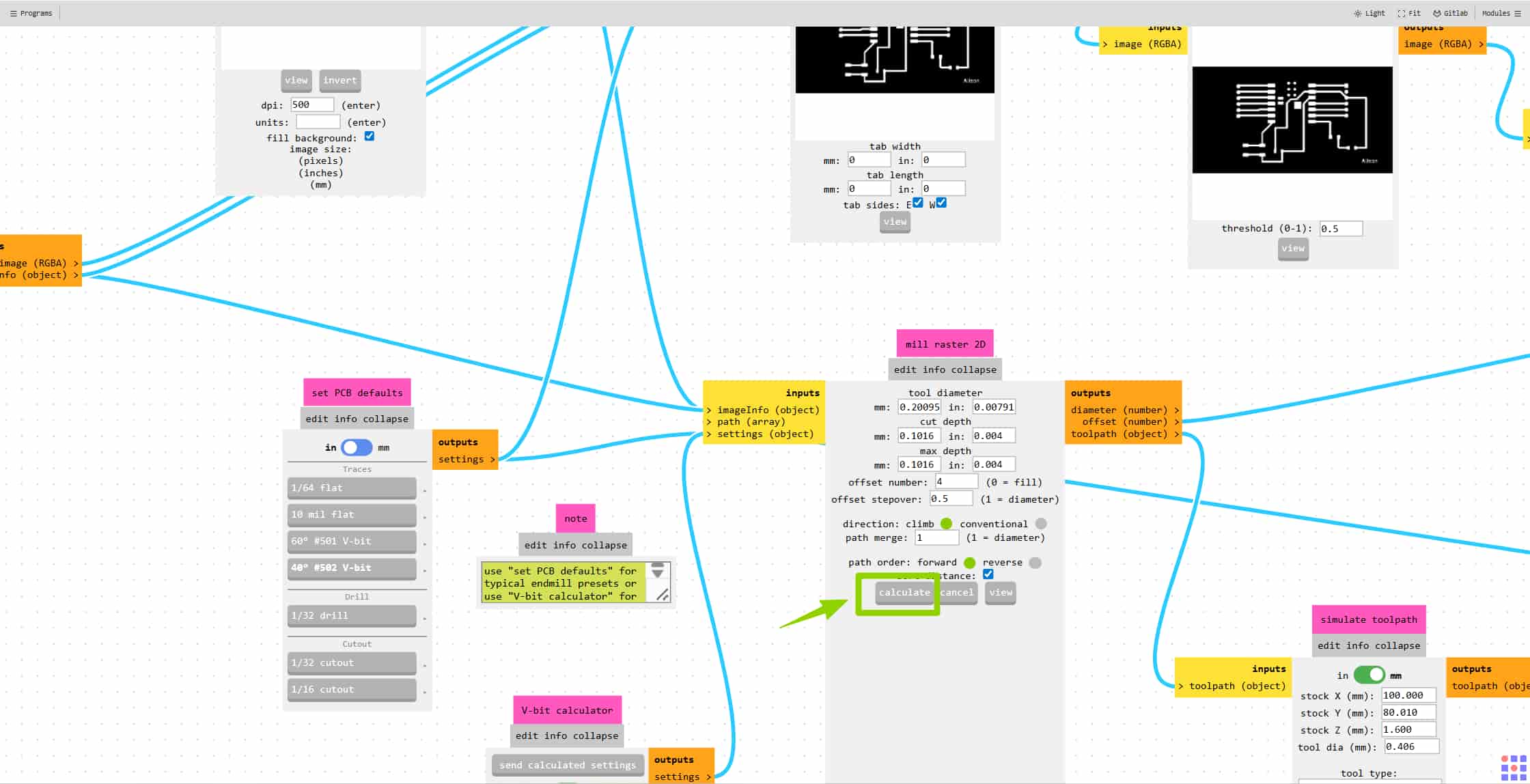
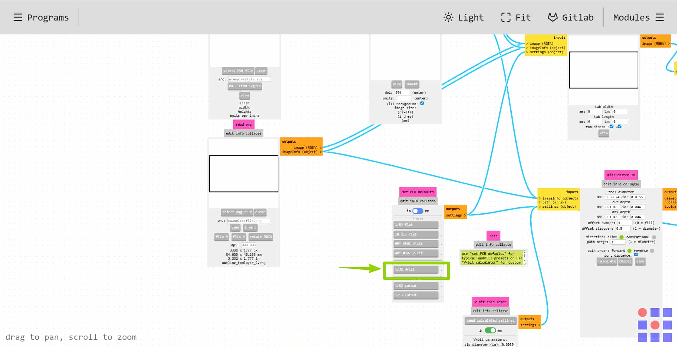
- Convert PNG → G-code using the Mods CE web tool. I clicked two buttons and adjusted parameters like cut depth and tool diameter — the group assignment has the exact values we settled on.
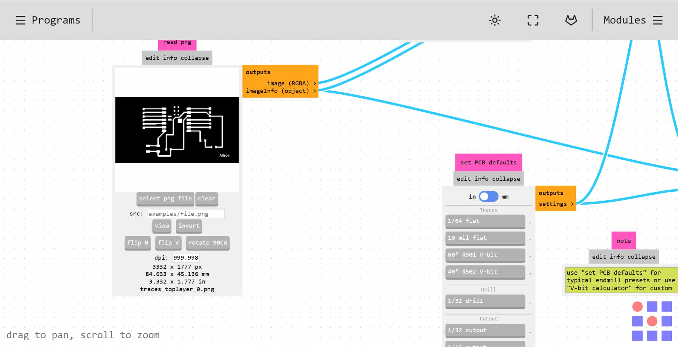
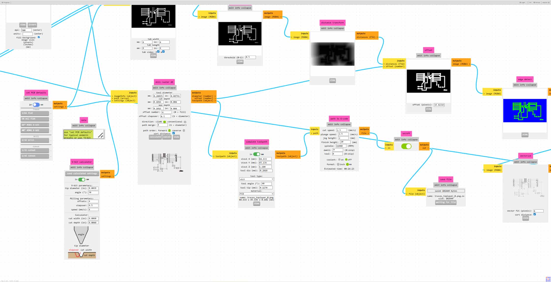
- Convert G-code to machine format using a Python script that reformats the file so our specific CNC controller can read it.
- Copy to USB and insert into the machine.
The key thing is to generate two separate G-code files, one for tracing, one for the outline, because they use different bits and different cut depths.
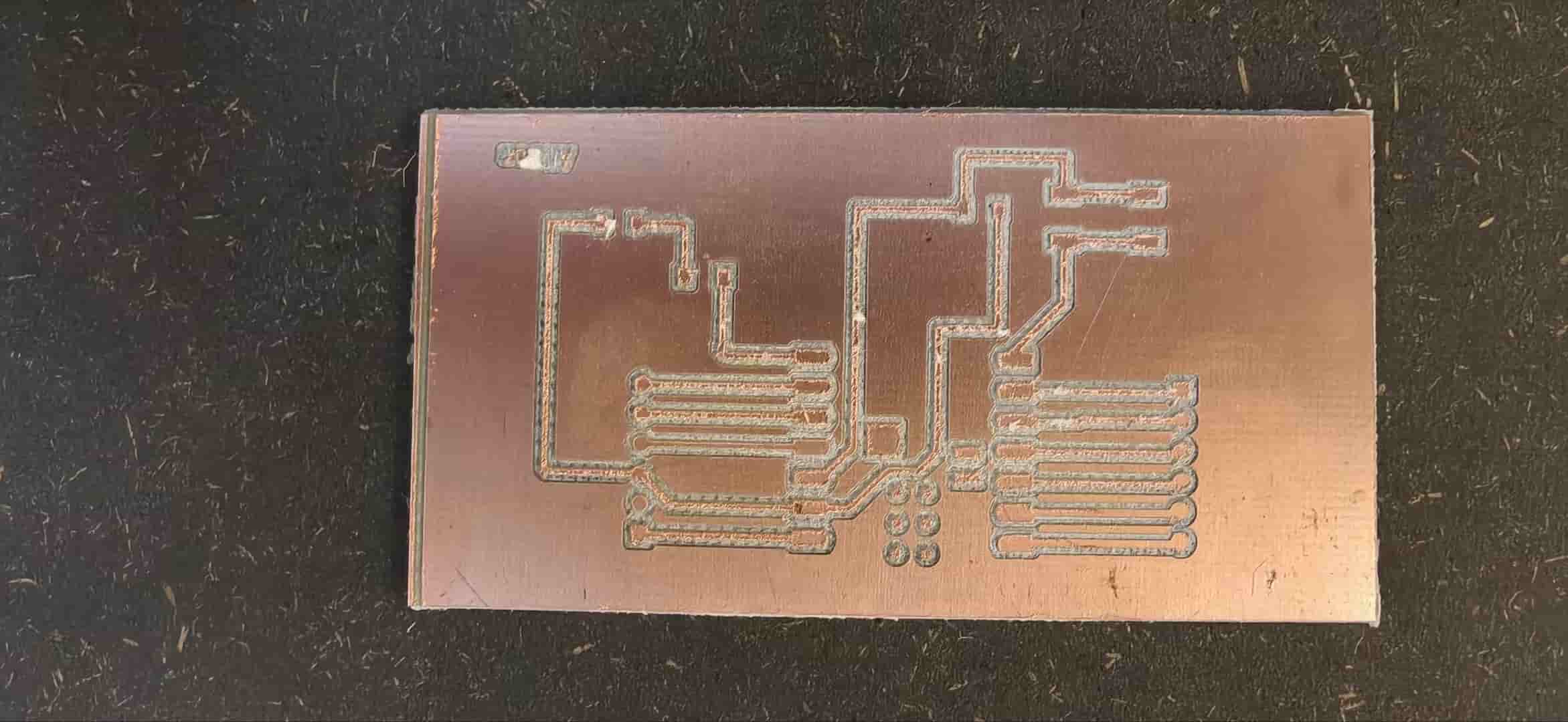
Part 4: Milling My First PCB
Setting Up the Machine
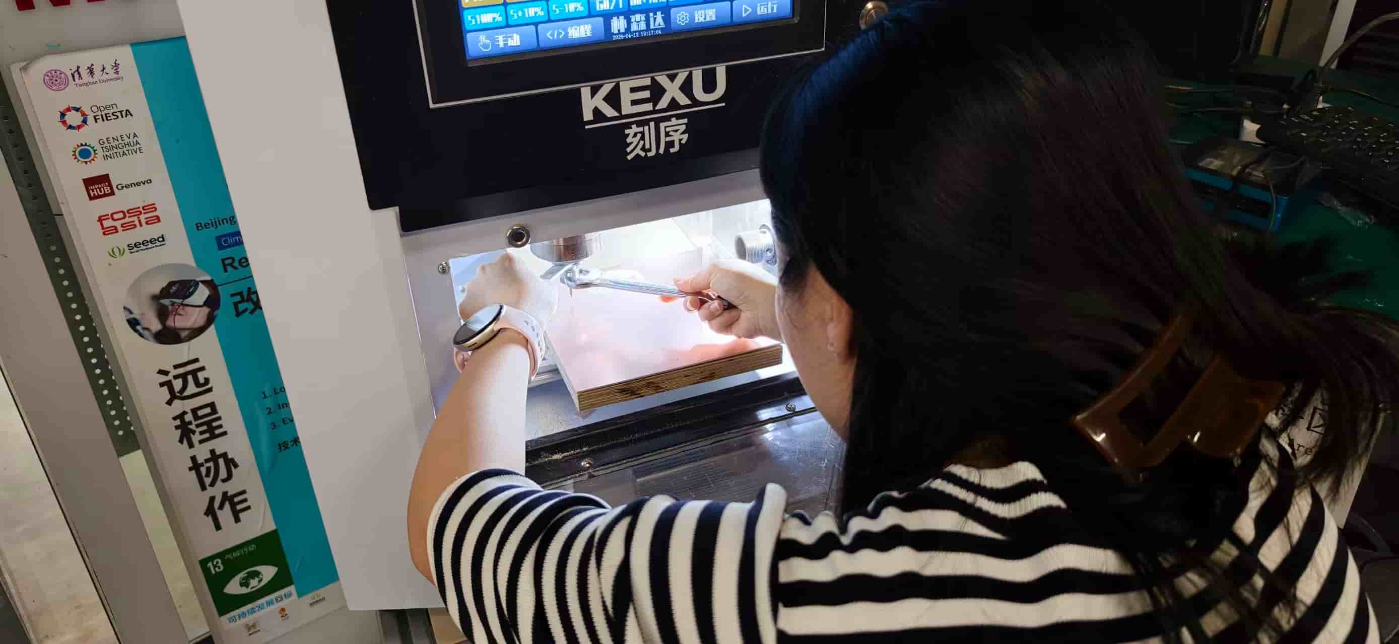
With the USB ready, I started on the CNC machine:
- Clean first. The spindle area had copper dust from previous runs. I brushed it out before doing anything else.(Since we have several members used it)
- Install the trace bit. The V-bit (sharp tip, for cutting traces) lives in the bottom-left tool position. To swap it in, I hold the button on the lower left to unlock the spindle, then use a wrench to unscrew the collet, note it's reverse-threaded, so you turn it the "wrong" way to loosen. The new bit clicked in and I tightened it back.
-
Fix the copper board. I placed the copper-clad board on the sacrificial wood base and secured it with double-sided tape.
-
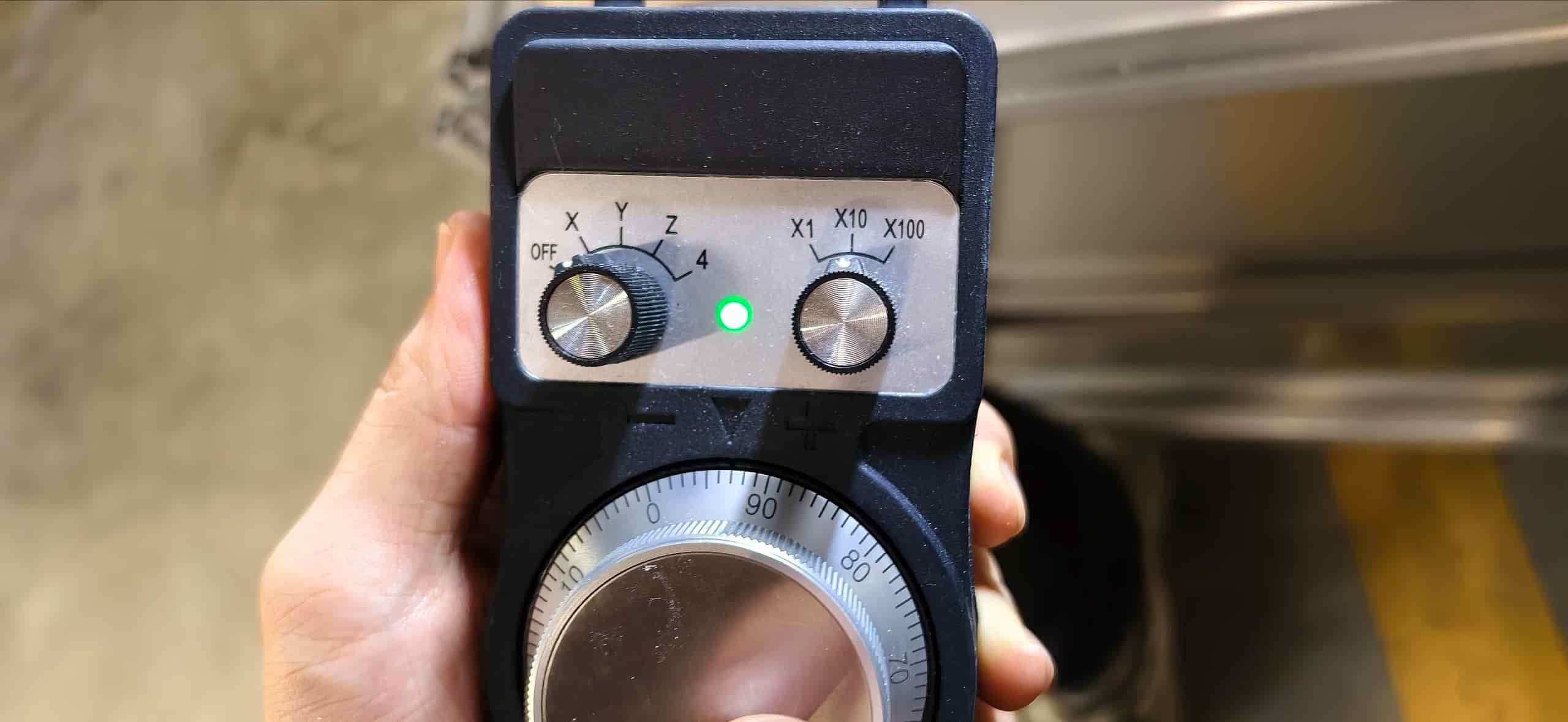
Set the zero point. Finding the right XYZ origin is important — X and Y set where the cut starts on the board, Z sets how deep the bit sits. I jogged the machine to a corner of the board and set origin. Important: do not press "return to origin" until you're sure about the orientation, or the machine will go somewhere unexpected.
Cutting the Traces
With the trace G-code loaded, I closed the door and pressed start. The machine made a satisfying high-pitched whirr and started cutting neat little channels through the copper.
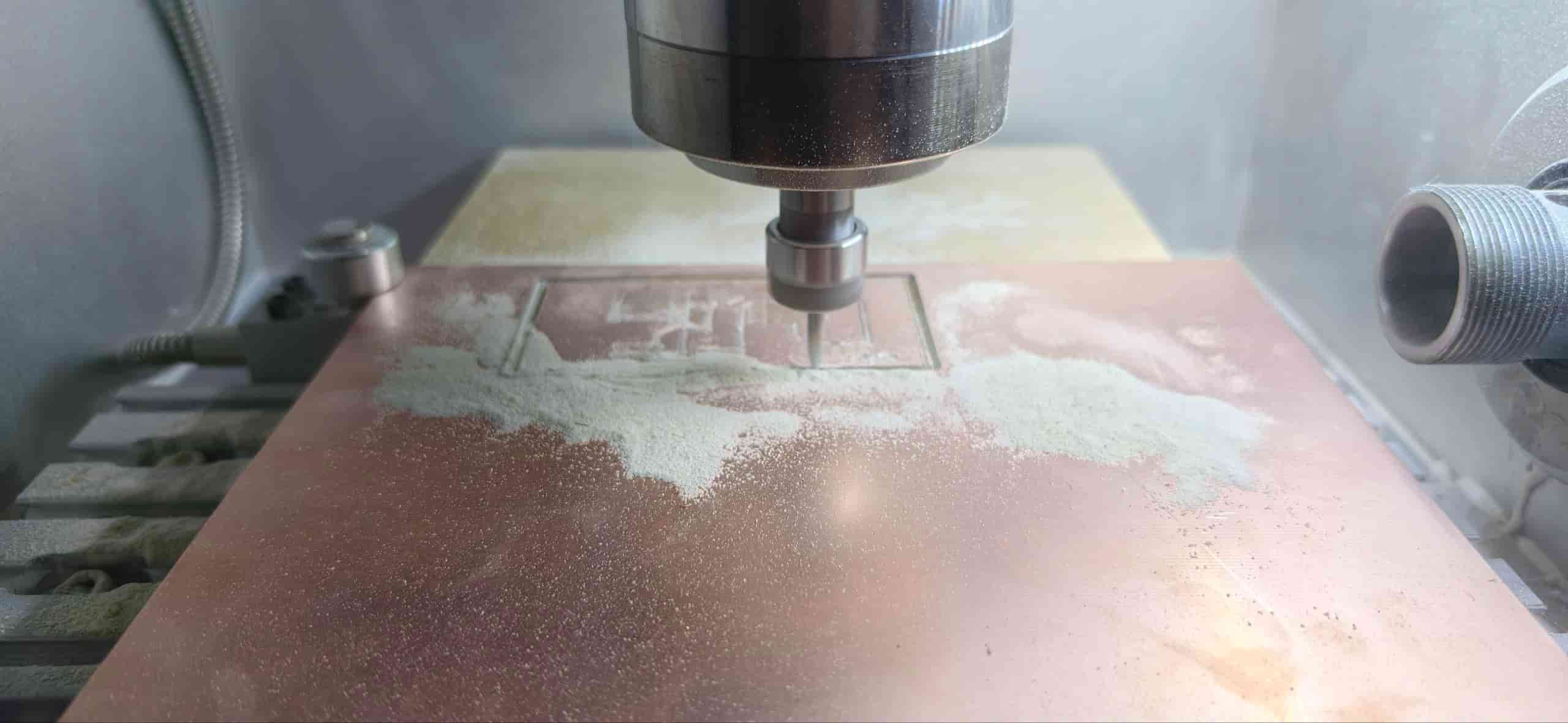
The trace cut went smoothly. After it finished, I did not move the board — this is critical, because the outline cut has to align exactly with the trace cut.
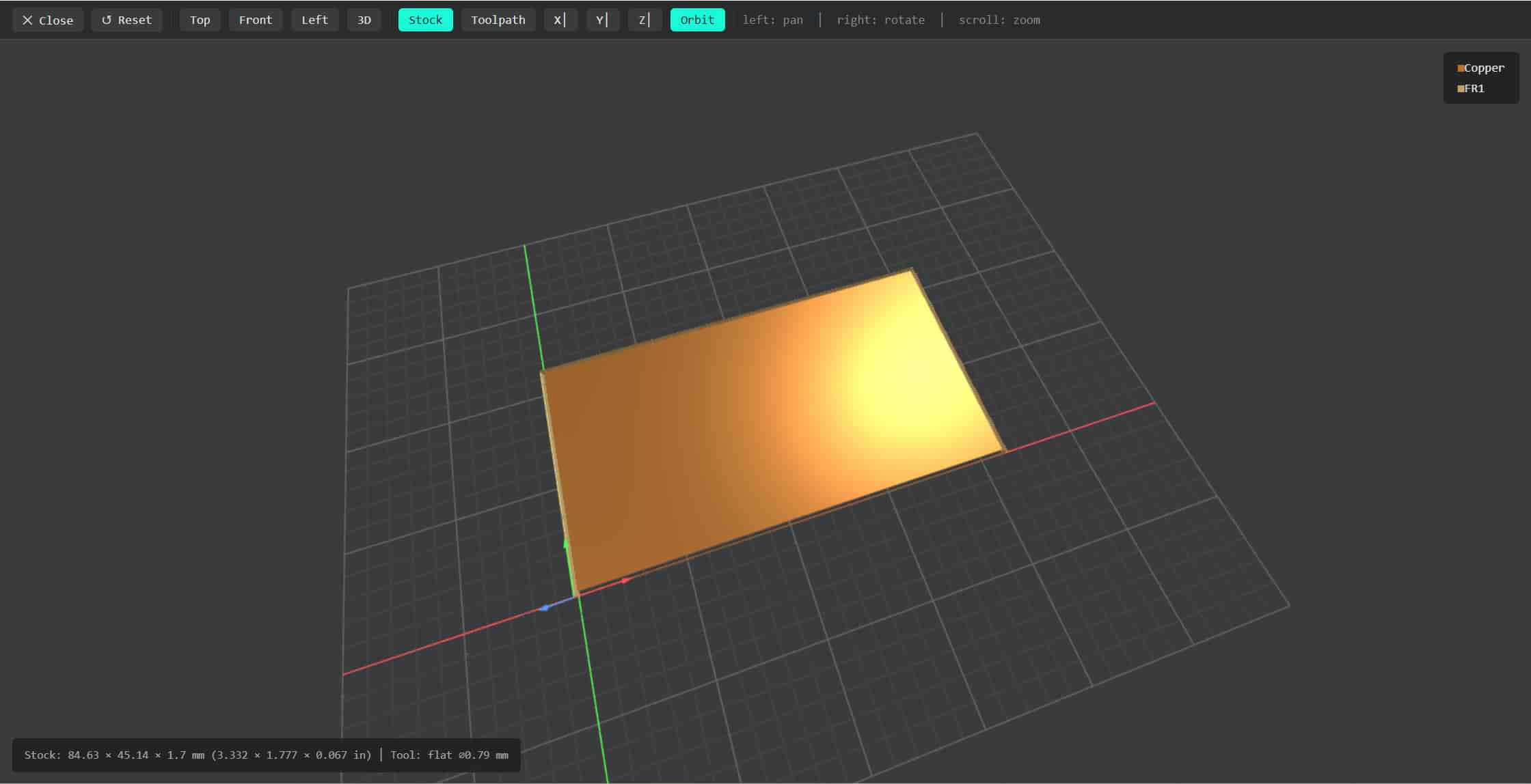
Switching Bits and Cutting the Outline
For the outline I swapped in the ball-end bit (flat bottom, for cutting all the way through). Same unlocking process — lower-left button, reverse-thread wrench. After changing the bit, I re-zeroed the Z axis only (X and Y stay the same), since different bits have different lengths.
Then I loaded the outline G-code and started cutting.
Partway through, the board started to shift. I could see the cut line drifting from where it should be — the double-sided tape hadn't held well enough under the stress of the deeper outline cut. I paused the machine, peeled up the board, added more tape, pressed it down firmly, re-found the position as accurately as I could, and restarted.
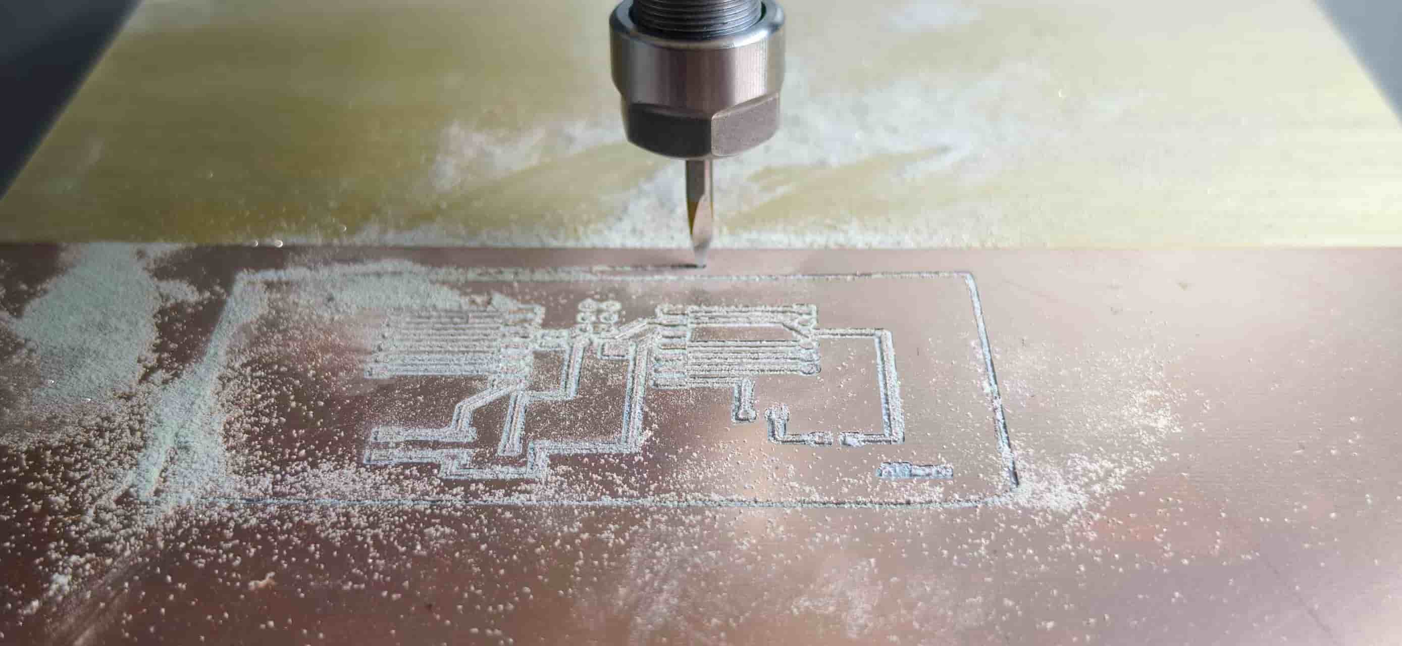
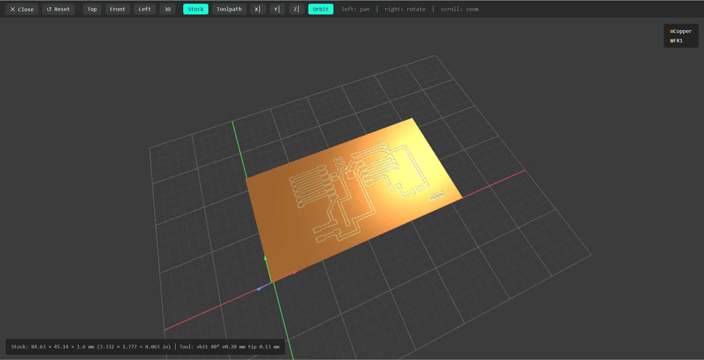
The second pass had a slight offset from the first, but the important thing was it cut all the way through cleanly, and the mismatch was only at the very edge, the inner traces were completely untouched.
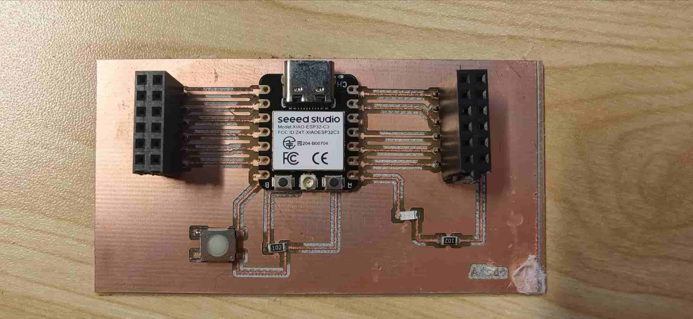
My first milled PCB. It looked great.
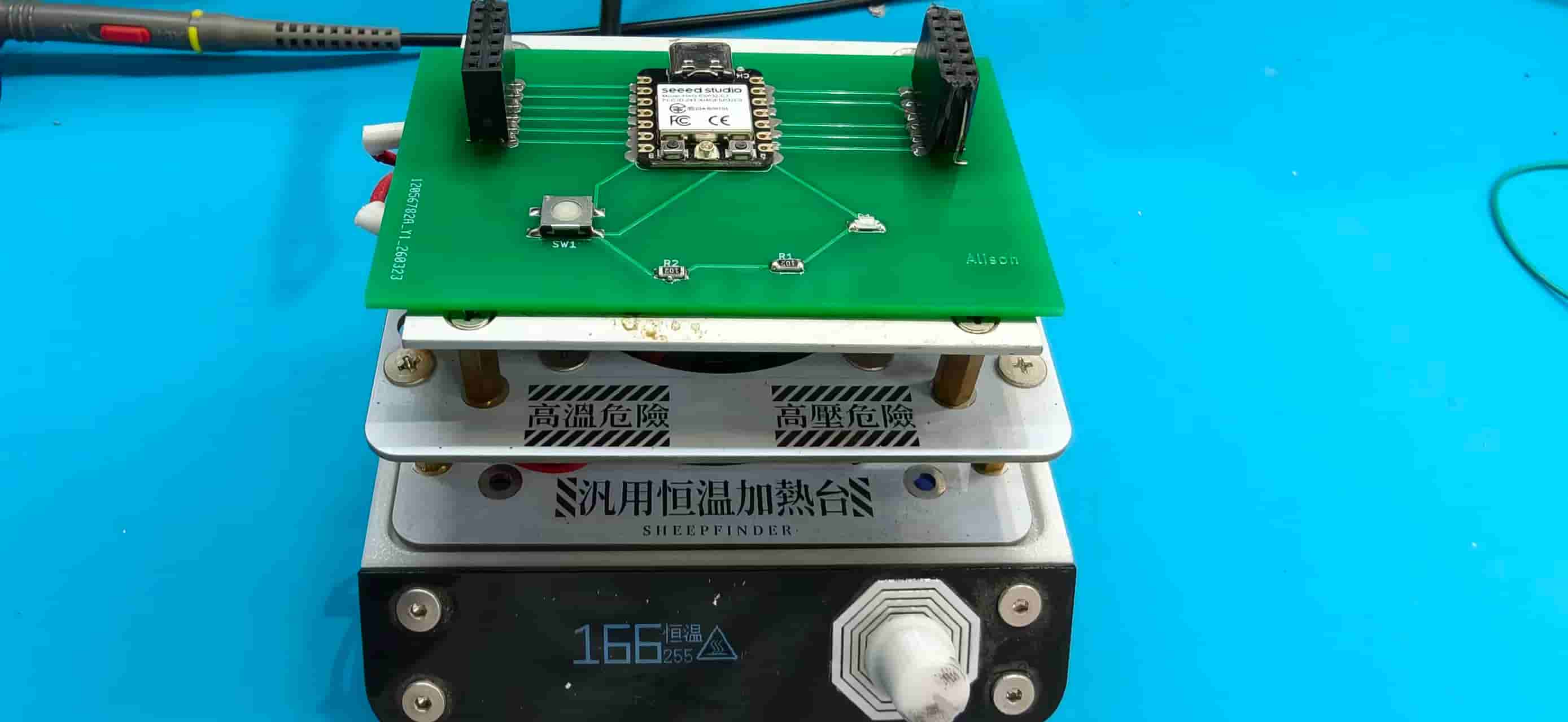
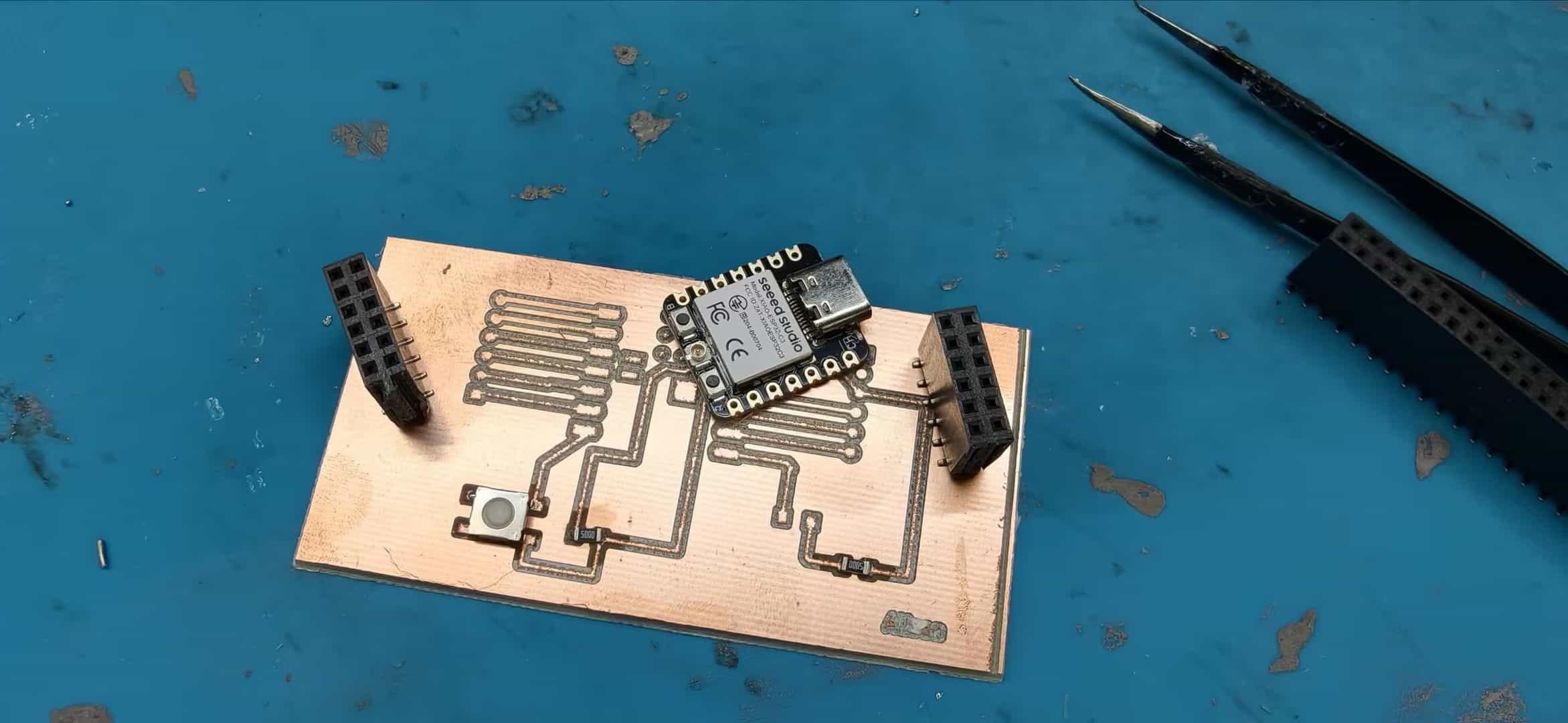
Part 5: Soldering with Solder Paste
For this board I used solder paste and a small reflow heating station instead of a soldering iron — much more convenient for SMD components.
The process:
- Squeeze a small, even amount of solder paste onto each pad. Don't overdo it — too much and you get bridges.
- Use tweezers to carefully pick up and place each component in the right position:
- LED (check the direction! The small arrow on the 1206 package marks the cathode)
- Resistors
- Tactile switch
- XIAO ESP32C3
- Socket header
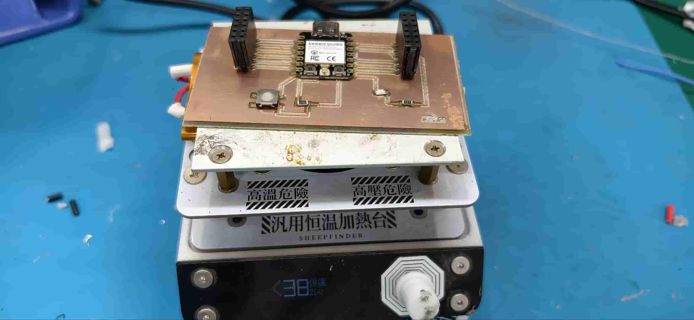
- Place the whole board on the heating station and power it on.
The station heats to 255°C. You can watch the solder paste transform in real time, it starts as a dull grey paste, then as it heats up it turns silver, starts to bubble slightly, and then retracts and snaps into a shiny point at each pad. It's genuinely satisfying to watch.
This time I was careful to double-check the LED orientation, the switch direction, and the resistor values before placing. Those were the exact mistakes from the first attempt.
Once the heating cycle finished, I switched it off and let the board cool down on its own, don't move it while the solder is still liquid.
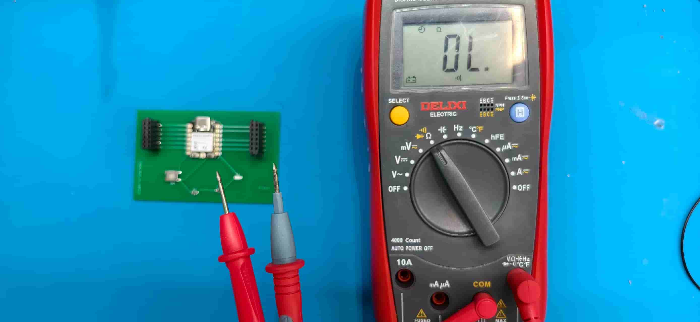
Part 6: Continuity Testing
Once the board cooled, I grabbed the multimeter and switched it to the Ohm / continuity mode (the beep setting). Two probes, touch both ends of a connection — if it's continuous, it beeps.
I went through the key nodes one by one.
Every single one beeped.
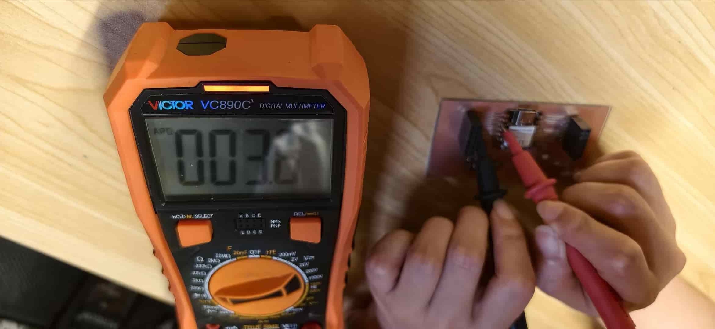
That little beep is one of the most satisfying sounds in electronics. It means the solder joints are good, nothing's broken, no cold joints, no open circuits. For a hand-placed reflow board on a milled PCB, this was a genuinely exciting moment.
Part 7: Programming and Testing
With a working board in hand, I plugged in the XIAO ESP32C3 and opened Arduino IDE. I wrote a simple test to blink the LED and respond to the button press:
const int buttonPin = D6;
const int ledPin = D7;

void setup() {

  pinMode(ledPin, OUTPUT);

  pinMode(buttonPin, INPUT);

}

void loop() {

  if (digitalRead(buttonPin) == HIGH) {

    digitalWrite(ledPin, HIGH);

  } else {

    digitalWrite(ledPin, LOW);

  }

}
Uploaded it, pressed the button — the LED lit up. Released, it turned off. Perfectly responsive.
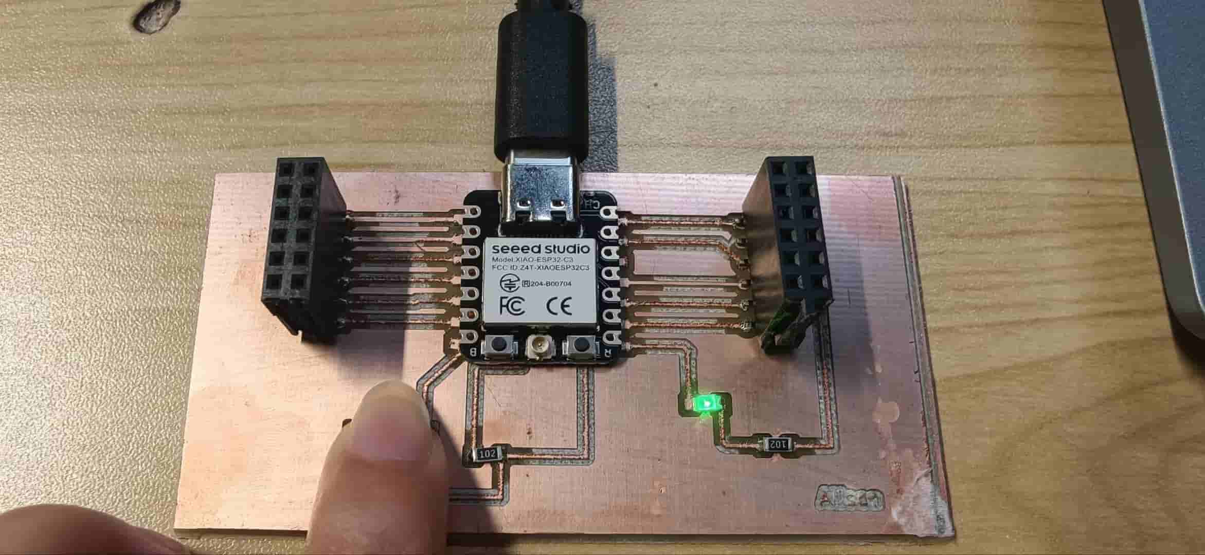
It worked on the first try. After all the fumbling with the JLC board, the missed ground line, the thin traces, the shifting board mid-cut, everything came together.
Reflections
A few things I'd do differently next time:
- Tape the board more aggressively before the outline cut. Clamps in addition to tape would help a lot.
- Triple-check LED polarity before placing. The 1206 marking is subtle enough to miss under stress.
- The solder paste + reflow approach is fantastic for SMD work, much easier than hand soldering small components, and the results look cleaner.