Group Assignment: PCB Production
Task
Complete the schematic and PCB design of the development board, and use the CNC for cutting. Submit the file to PCB Design house.
In-House PCB Milling: Design Rules
Machine and Tools
For our in-house PCB production, we use a KEXU. This machine is mainly used for precise prototyping work, such as PCB milling is one of its key applications in our lab.
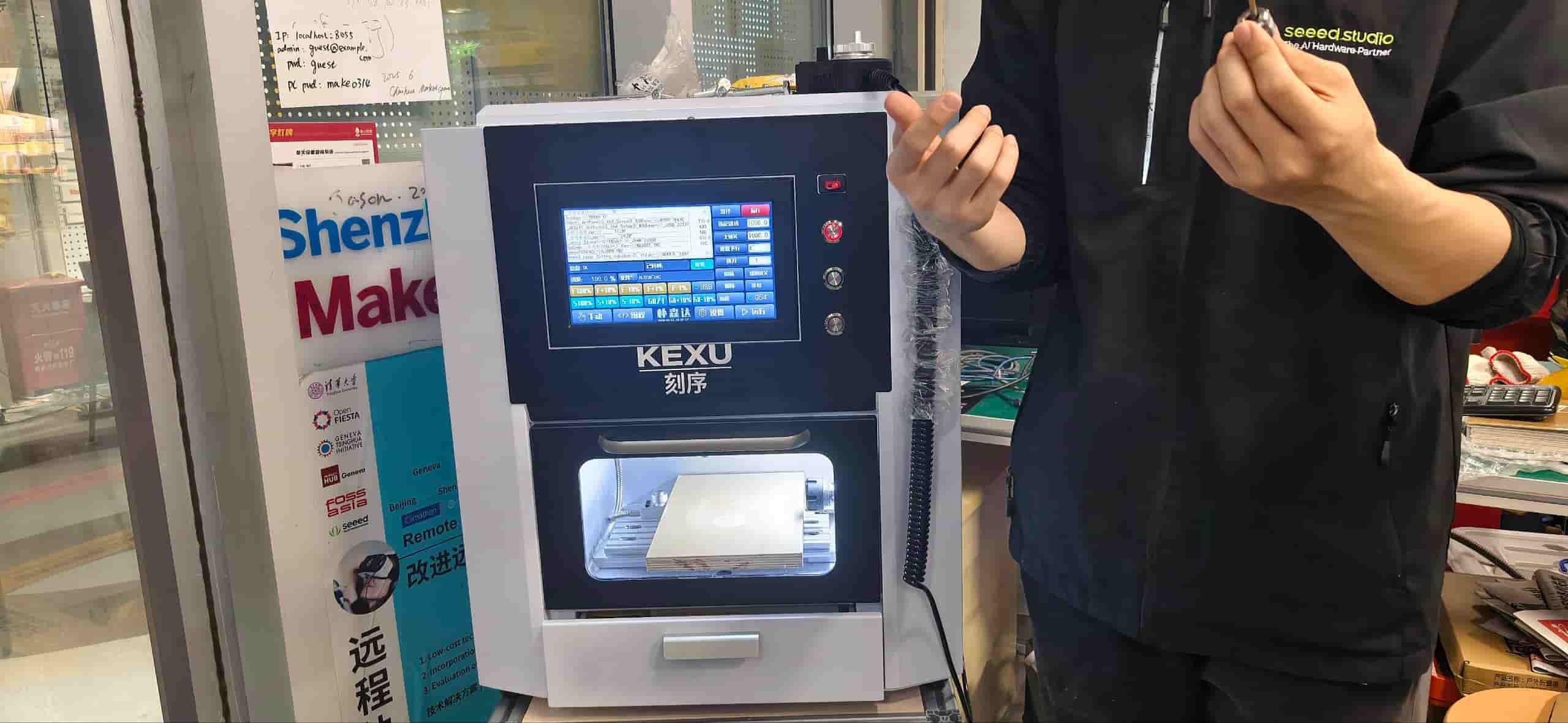
Here are its basic specs:
| Specification | Exu Turbo (3-Axis) |
|---|---|
| Model | Exu Turbo (3-Axis) |
| Overall Dimensions (L × W × H) | 550 × 490 × 620 mm |
| Travel (X/Y/Z) | 190 × 120 × 110 mm |
| Relief Carving Area | 200 × 120 mm |
| Machine Weight | 88 kg |
| Machine Body Material | Aluminum Alloy |
| Machining Speed | 0–4000 mm/min |
| Spindle Cooling | Water Cooling |
| Spindle Power | 800W |
| Spindle Speed | 0–24,000 RPM |
| Drive System | Hybrid Servo |
| Linear Guide Rails | Imported Taiwan Square Rails |
| Lead Screw | Imported Taiwan Lead Screw |
| Tool Holder Capacity | 1–6 mm |
| Rated Voltage | AC220V / 50–60Hz |
| Total Machine Power | 1.0 kW |
| Control System | Intelligent 4-Axis Linkage (7-inch Touch Screen) |
| Data Transfer | Wi-Fi, Mobile Hotspot, USB Drive |
Material
We use standard single-sided copper-clad boards:
- Type: FR-1 / FR-4 epoxy glass fiber
- Board thickness: 1.6 mm
- Copper layer thickness: 35 μm (1 oz)
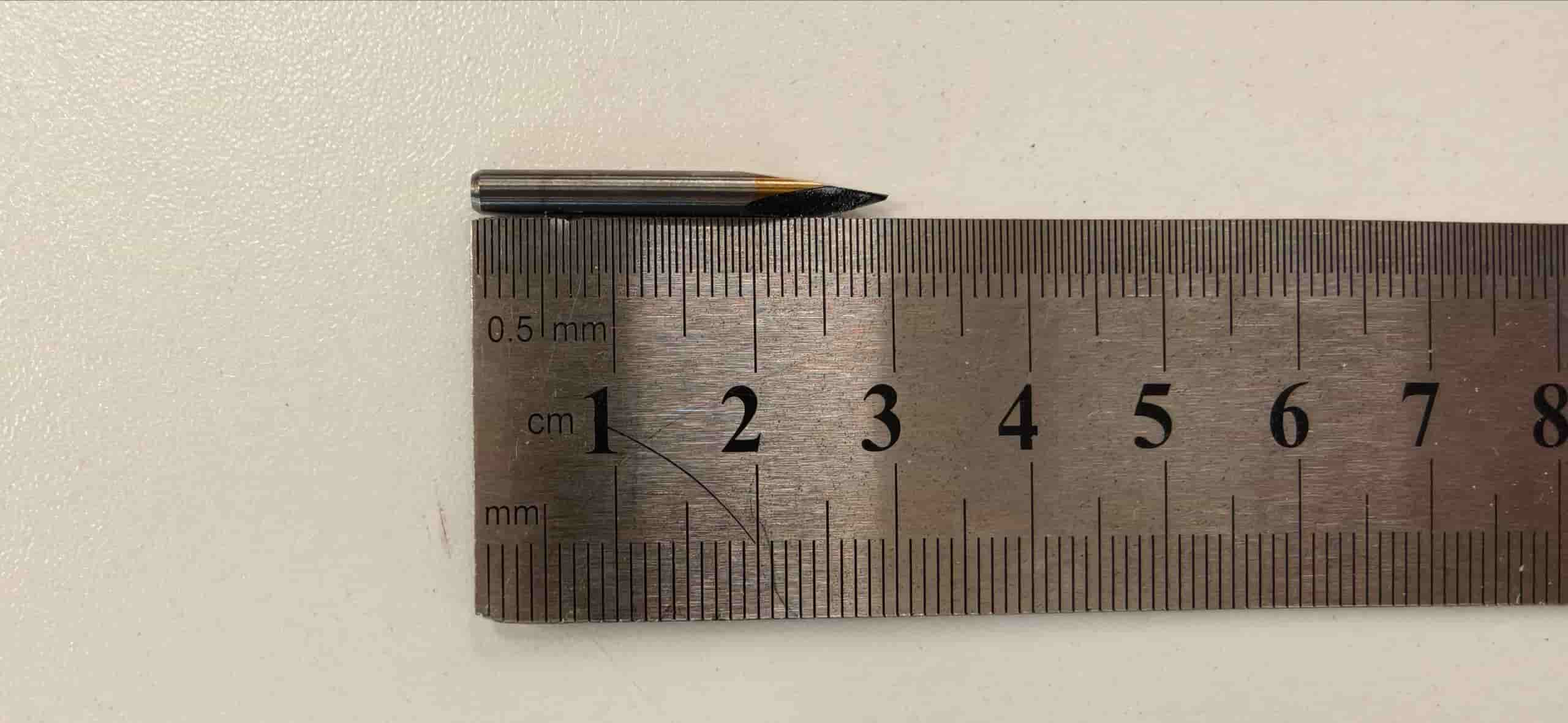
And using 40° #502 V-bit for tracing
Finding the Right Parameters
The goal here was not just to pick some settings and run, it was to find parameters that produce clean, reliable results on our specific machine and material. Too aggressive and you snap the bit or tear the copper; too conservative and the job takes forever without much benefit.
We tested different combinations and landed on the following:
| Parameter | V-bit (Tracing) | Ball-end (Outline Cutting) |
|---|---|---|
| Feed Speed | 4 mm/s | 4 mm/s |
| Spindle Speed | 14,000 rpm | 14,000 rpm |
| Offset Number | 4 | 4 |
| Offset Stepover | 0.2 mm | 0.2 mm |
| Cut Depth | 0.23 mm | 0.45 mm |
| Tool Diameter | 0.3 mm | 1.5 mm |
The cut depth of 0.23 mm for tracing is just enough to remove the copper without going too deep into the substrate. For the outline, 0.45 mm per pass cuts through the board cleanly in multiple passes without stressing the bit.
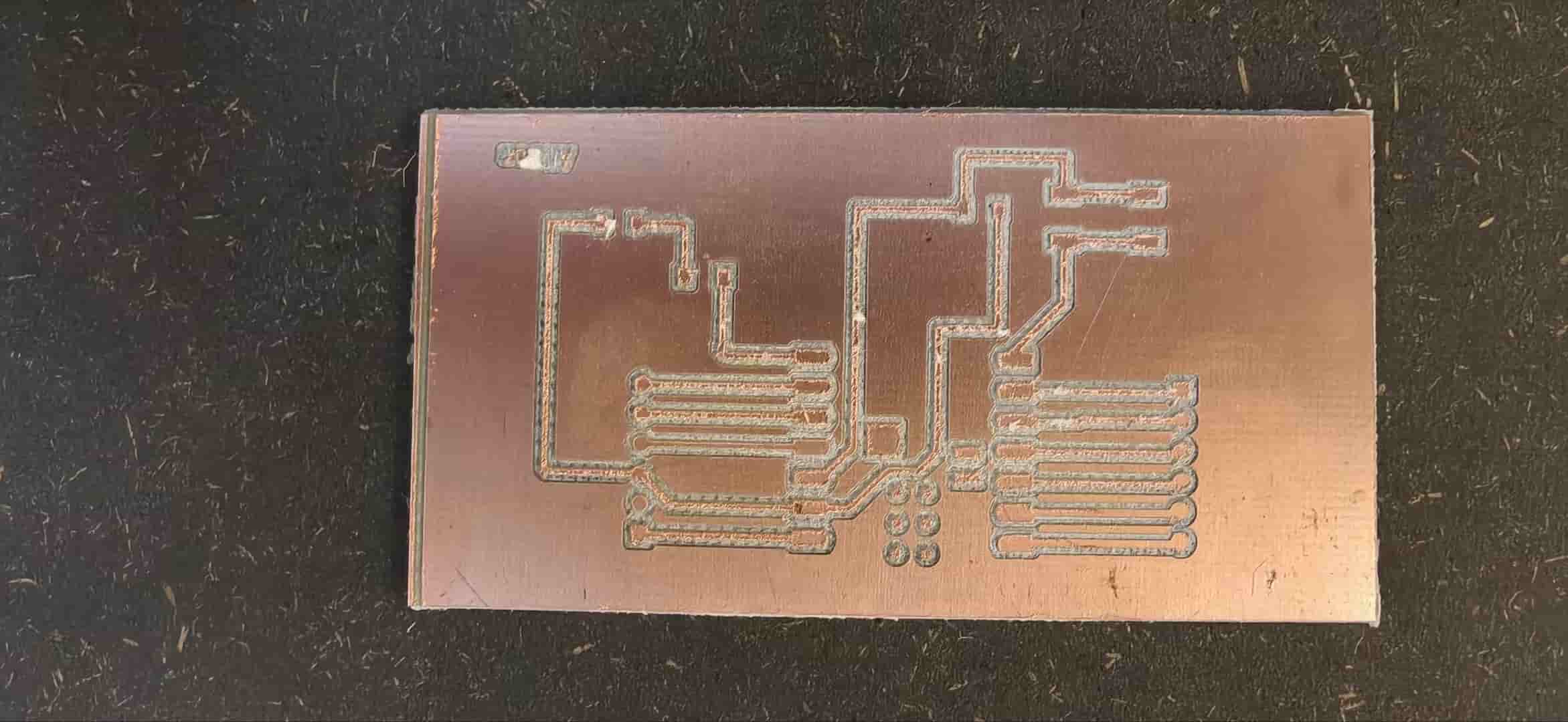
Result
With these parameters, the traces came out clean and the board outline cut through without issue. The finished board was ready for population.
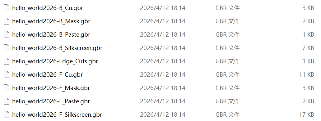
Submitting a PCB Design to a Board House
When I milled my PCB in-house back in Week 6, I only needed two Gerber files:
F_Cu.gbr— the copper trace layerEdge_Cuts.gbr— the board outline
That's enough for the milling machine. But a board house needs more, because they're handling multiple fabrication steps: etching, drilling, solder masking, and silkscreening. Each of those steps needs its own file.
After looking into it, the minimum set for board house submission is:
| File | Purpose |
|---|---|
F_Cu.gbr | Front copper traces |
Edge_Cuts.gbr | Board outline |
B_Mask.gbr | Back solder mask (also contains drill info) |
F_Mask.gbr | Front solder mask |
F_Silkscreen.gbr | Component labels and markings on the surface |
Before this assignment, I hadn't thought much about solder mask or silkscreen as separate layers — they just appeared on finished boards I'd seen. Understanding what each layer actually does made the whole PCB manufacturing process click for me.
Solder mask is the colored polymer coating (usually green, but it can be any color) that covers the copper except at the pads. Its job is to prevent solder bridges between traces during assembly and to protect the copper from oxidation. Without it, every trace would be exposed and prone to shorting during soldering.
Silkscreen is the printed text and symbols on the board surface — reference designators like R1, C2, polarity markings, and labels. It's there mainly for assembly guidance and debugging. Without silkscreen, placing components correctly on a dense board becomes much harder.
The drill file (often embedded in B_Mask.gbr or exported separately as .drl) tells the board house where to drill holes, how large each hole should be, and whether each hole is plated (for vias and through-hole pads) or non-plated (for mechanical mounting).
Once I understood what each file does, generating them from KiCad was straightforward — I already had the design from Week 6, so it was mostly an export exercise.
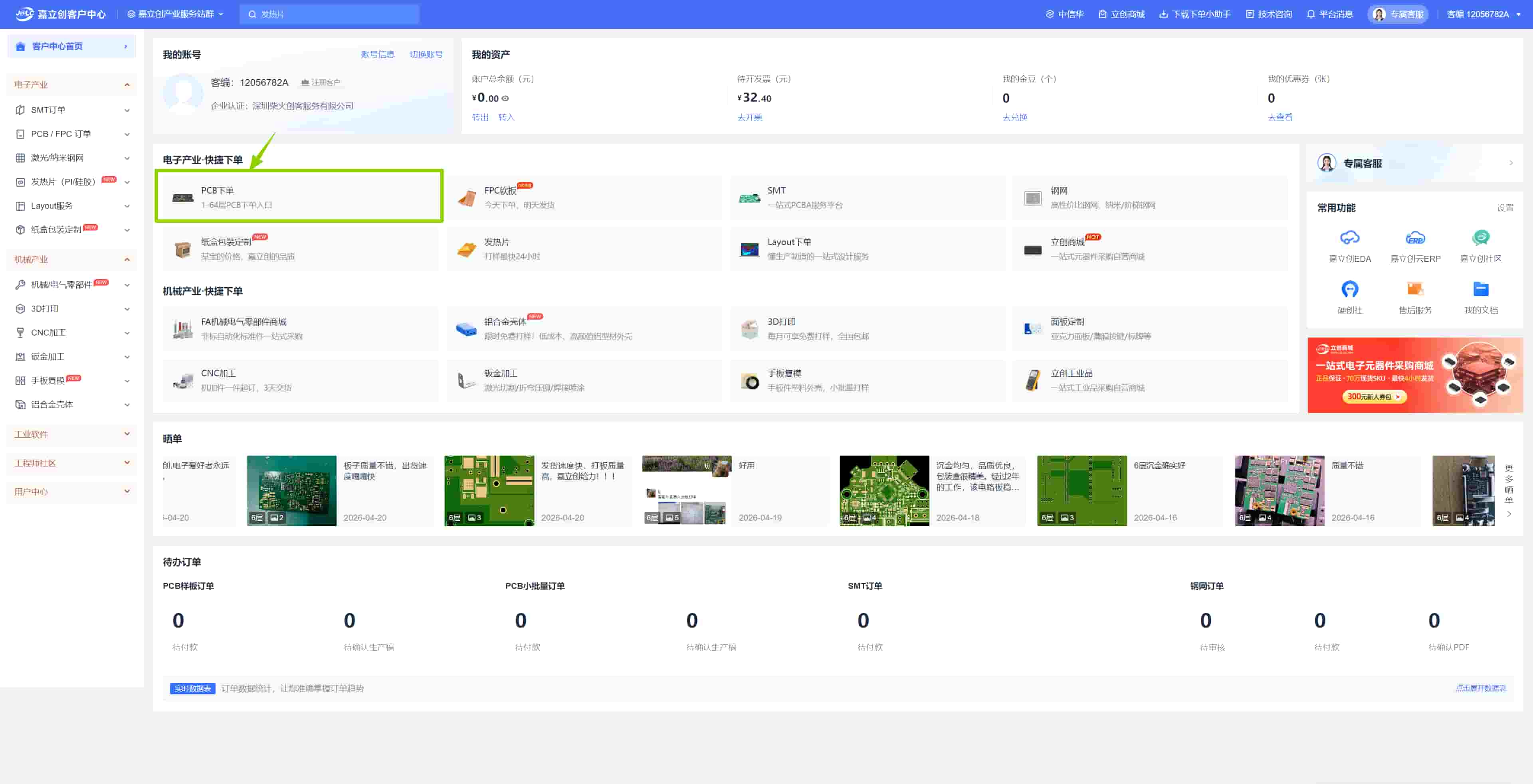
Ordering at JLC
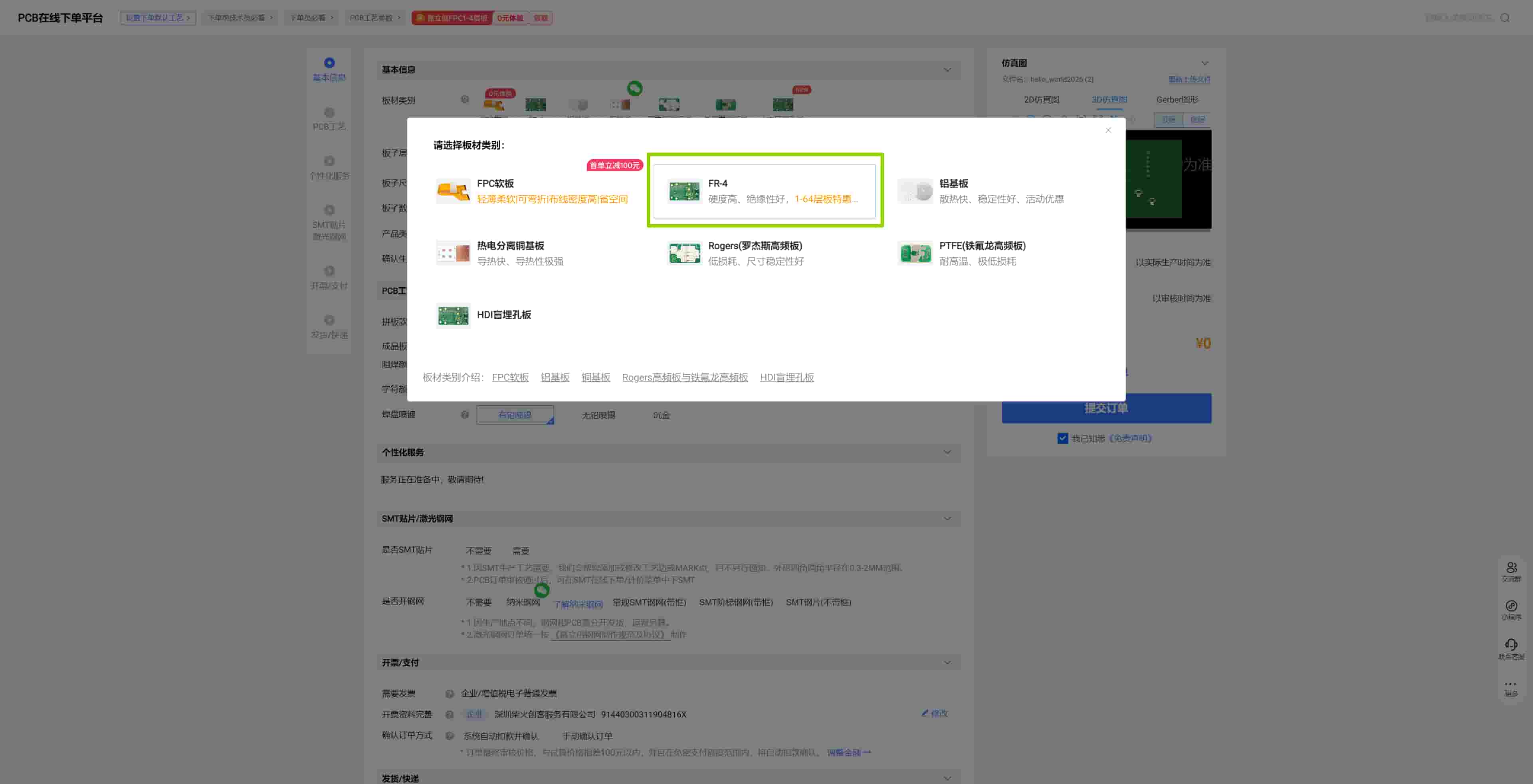
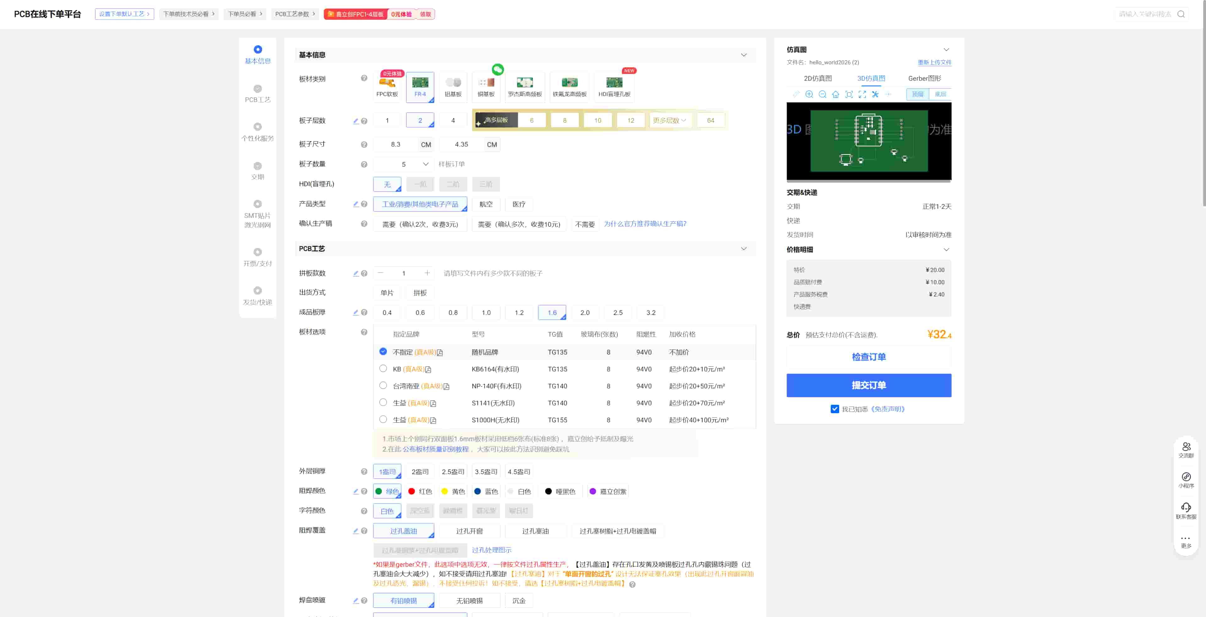
I heard JLC long time ago, and this time finally to try my design at JLC Technology Group (JLC), an online board house based in Shenzhen. Our instructor Matthew introduced us to it; they're fast and inexpensive.
Uploading and Setting Parameters
After uploading the zipped Gerber files, the ordering page asks for board specifications. Our basic settings were:
| Parameter | Value |
|---|---|
| Board Material | FR-4 |
| Board Size | 6.1 × 3.6 cm |
| Layer Count | 2 |
| Board Thickness | 1.0 mm |
| Use Grade | Consumer |
| Product Type | Economical |
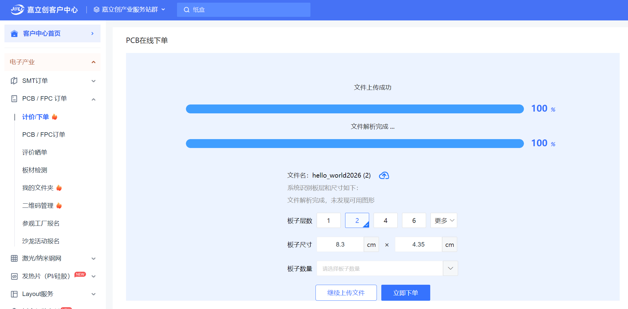
The system checks the files automatically. If anything looks wrong with the design, a staff member follows up with a phone call to clarify, which feels reassuring for a first order.
Confirming the Preview
Before production starts, JLC shows you a side-by-side comparison: your uploaded design on one side, their production draft on the other. There's also a 3D view. This step is worth spending a few minutes on — it's the last chance to catch any layer issues before the boards are made.
Production and Delivery
We ordered 5 boards and paid around ¥40 RMB (~$6 USD). The order was placed on March 23. I received on March 25, really fast.
The Finished Boards
After receiving the boards, we soldered the components and tested them. Everything worked.
Comparing the milled version and the board-house version side by side is interesting. The milled board is rougher at the edges and has no solder mask or silkscreen, but it's faster to iterate on. The JLC board looks clean and professional, and the solder mask makes assembly easier.
Both have their place — milling for rapid prototyping and testing, board house for a cleaner final version.