Group assignment
Individual assignments

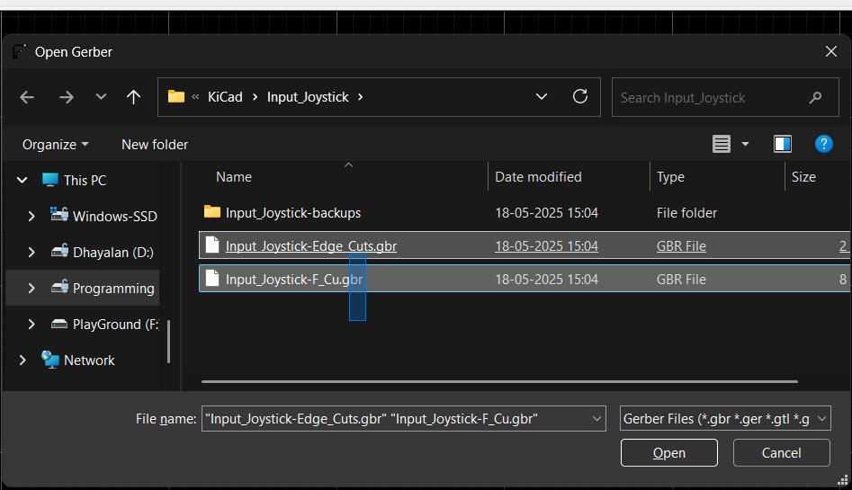
In the Electronics Design Week, I successfully designed a custom PCB layout using KiCad. After completing the schematic and PCB routing stages, I proceeded with the fabrication process, which involved preparing the Gerber files, verifying design rules, and exporting the layout. This marked the transition from design to actual hardware realization.
Electronics Design Week Assignment
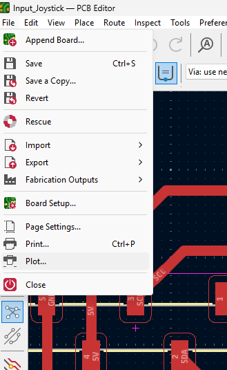
In the PCB Editor, I navigated to the "File" menu and selected the "Plot" option to generate the necessary output files. This step is essential to prepare the Gerber files, which are used for PCB fabrication. I ensured the correct layers were selected before proceeding with the plot.
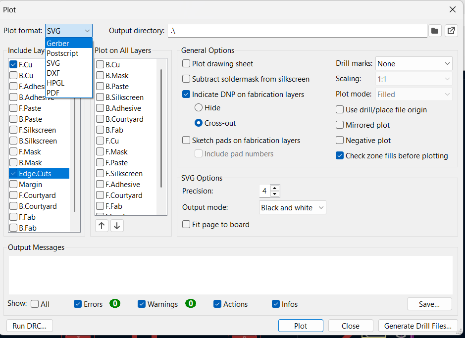
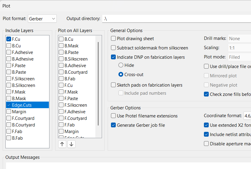
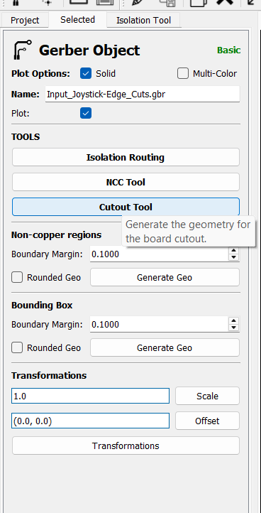
In the Plot option of the PCB Editor, I generated the Gerber files, which are essential for PCB fabrication. I selected the necessary layers such as F.Cu, and Edge.Cuts ensuring all relevant details were included for accurate manufacturing output.

FlatCAM is an open-source software used to convert Gerber and drill files into G-code, which is required for PCB milling using CNC machines. It is especially useful in PCB prototyping, allowing users to create isolation routes, drill paths, and board outlines. FlatCAM supports various CNC milling operations and offers customization in tool diameter, cut depth, feed rate, and more. It provides a visual preview of tool paths, making it easy to prepare PCBs for fabrication without the need for chemical etching.
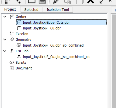
In FlatCAM, import the F.Cu and Edge.Cuts Gerber files by selecting “File → Open Gerber.” Load the top copper layer (F.Cu) and the board outline (Edge.Cuts). Both layers will appear on the canvas and project panel. Ensure alignment before proceeding with further PCB fabrication steps like isolation routing.
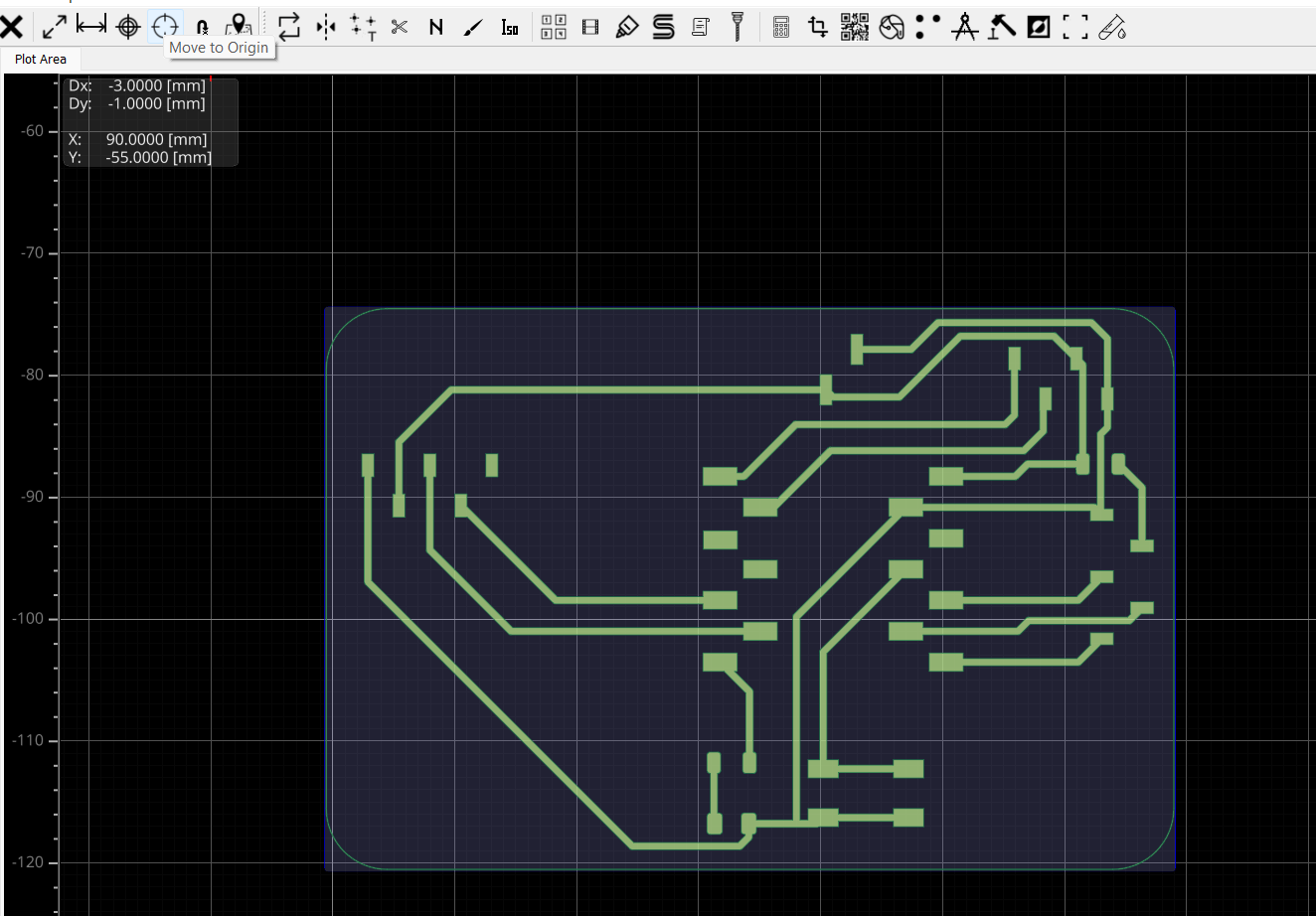
After importing the F.Cu and Edge.Cuts files in FlatCAM, the layout appeared off-screen. To fix this, I realigned the design to the origin using the "Align Origin" tool. This ensured the copper traces and board outline were correctly positioned for accurate toolpath generation and smooth PCB fabrication.
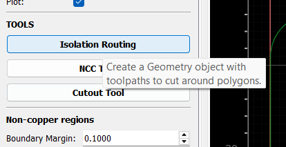
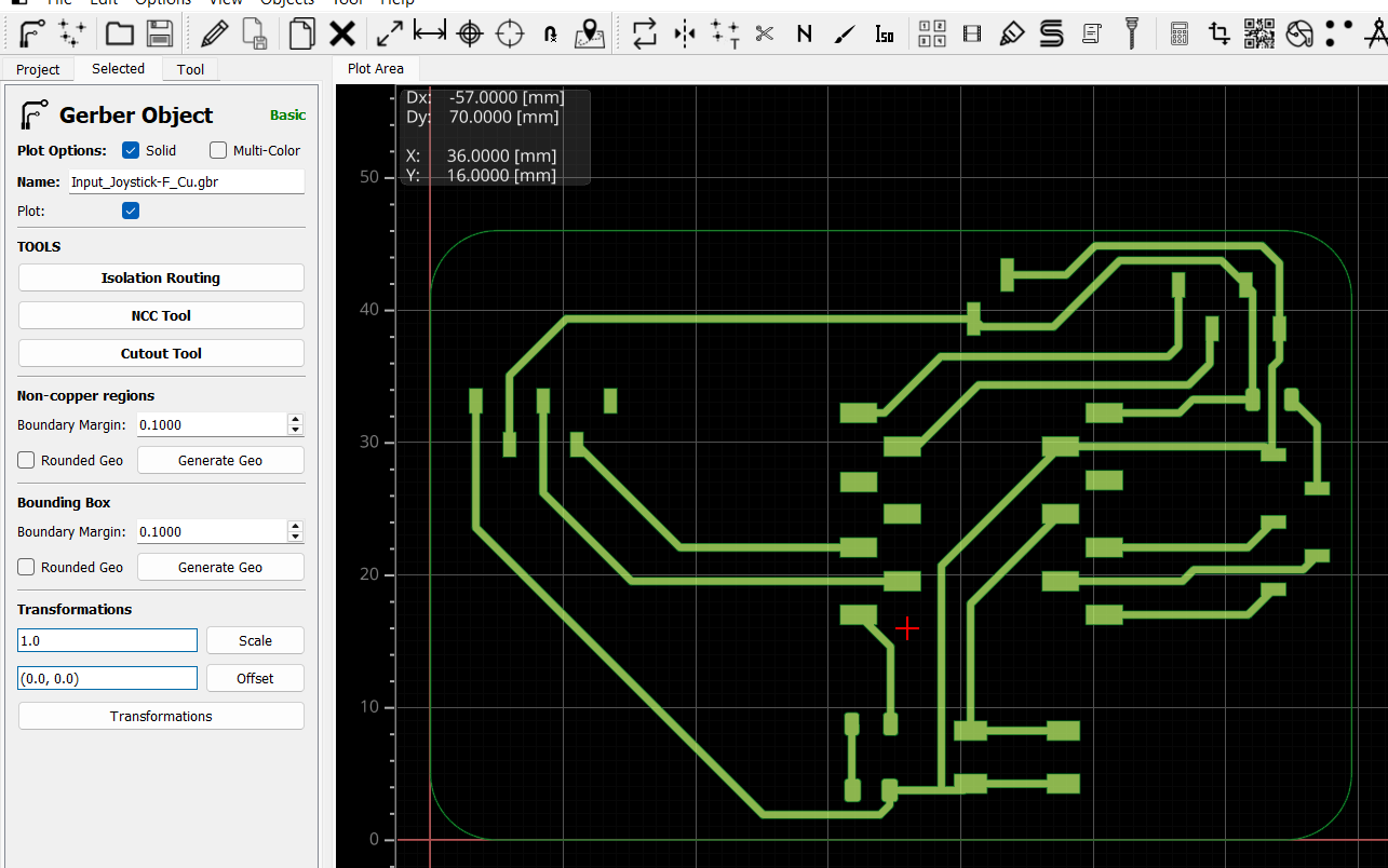
Then I entered the Properties panel in FlatCAM to select the Isolation Tool. This step is crucial for defining how the copper will be isolated from the board, ensuring clean traces.
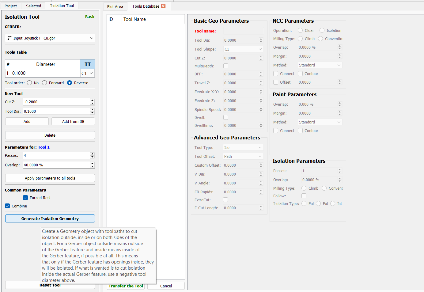
Then I checked the Tool Database in FlatCAM to get clarity on the available milling bits and their specifications. This helped ensure I selected the correct tool diameter, cut depth, and feed rate based on the PCB material
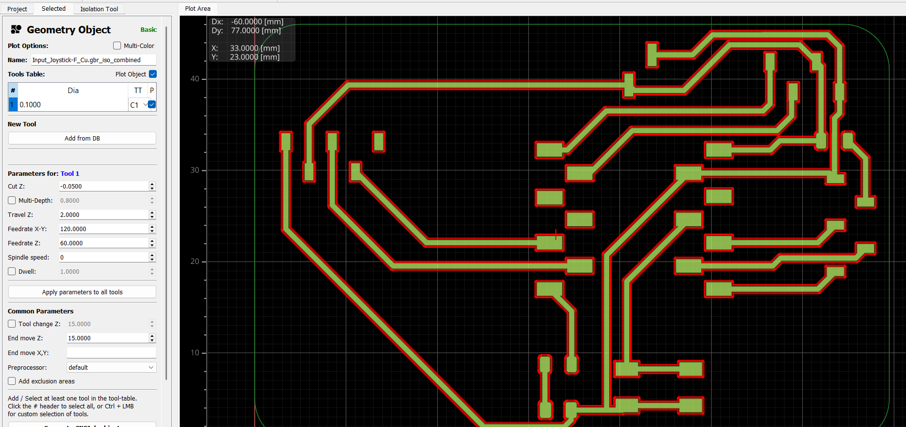
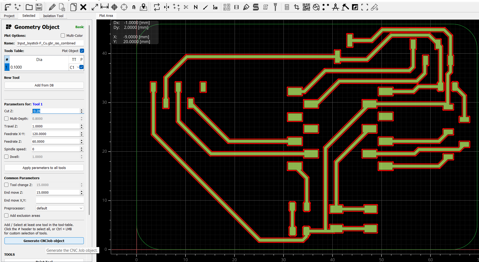
Since there was no preloaded Tool Database in FlatCAM, I manually created the required tool settings. I generated the geometry by defining key parameters such as tool diameter, cut depth, spindle speed, and feed rate. These values were chosen based on my PCB requirements and the specifications of the available end mill.
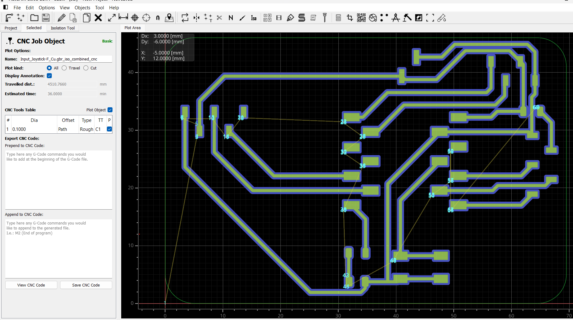
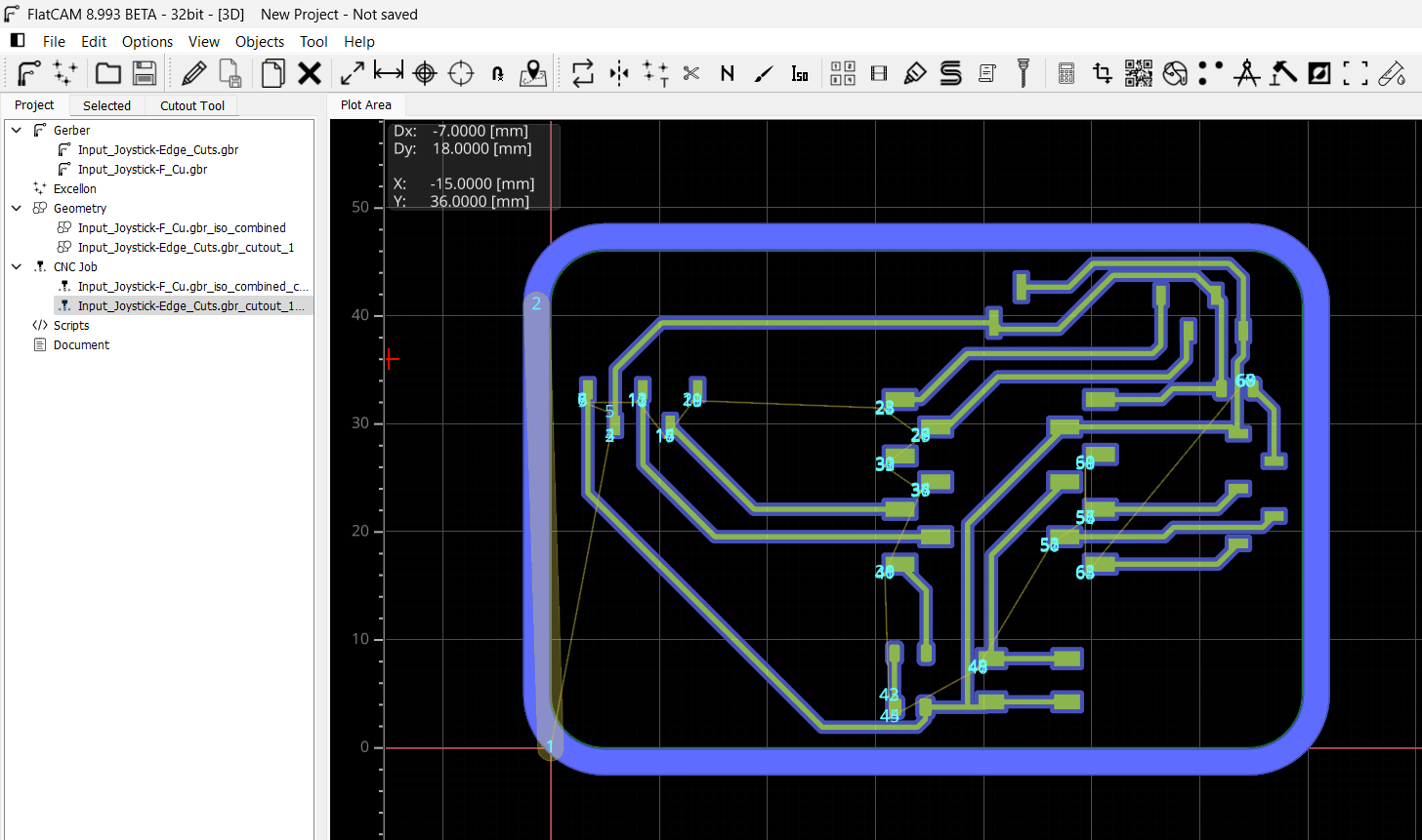
Then I generated the Edge Cut path, and after that, I viewed the CNC code (G-code) generated for the milling process. This code includes the exact tool movements, depths, and coordinates required by the CNC machine to cut the board outline accurately
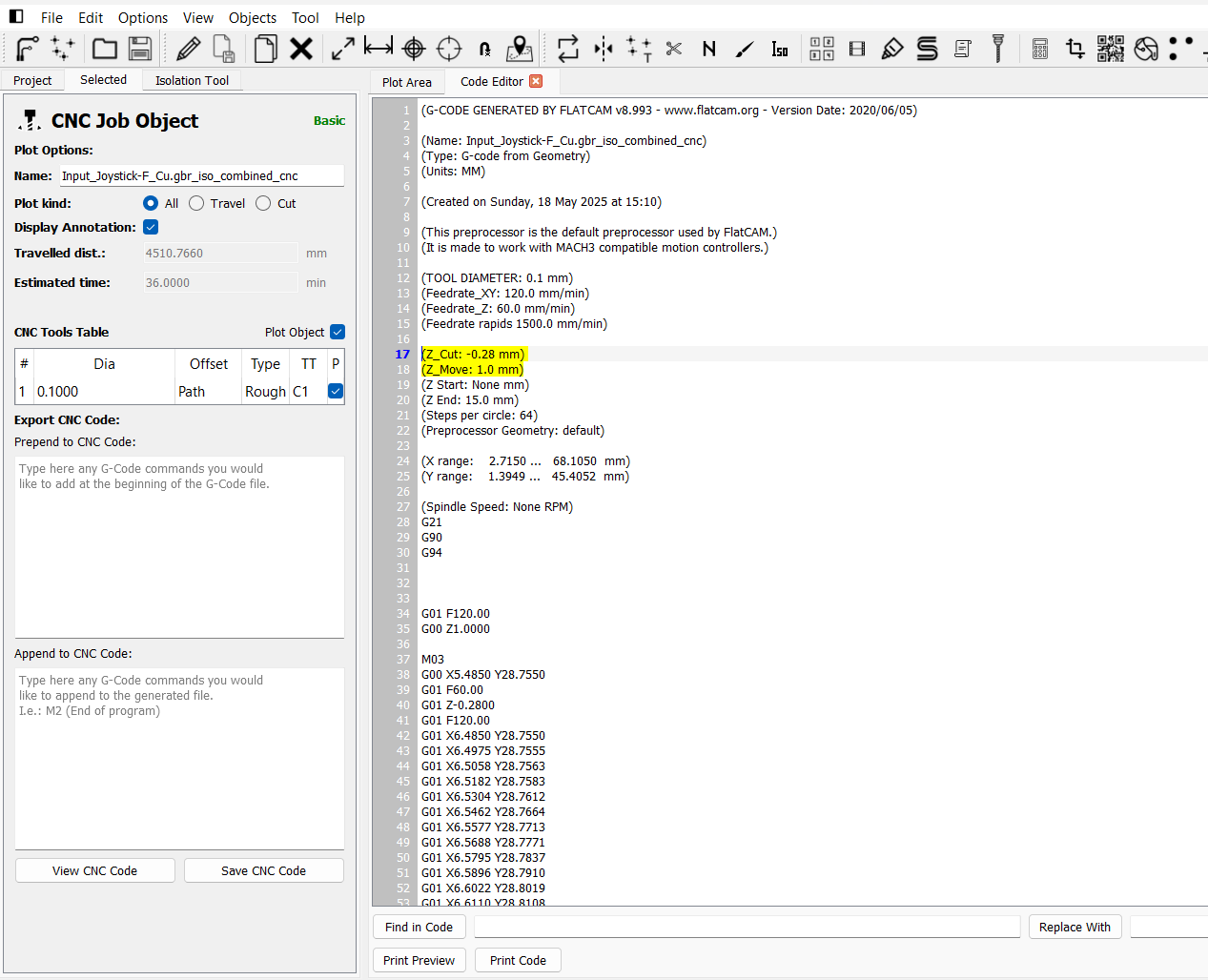
Reviewing the CNC code ensures that all tool paths, cut depths, and coordinates are correctly defined. This step is crucial to avoid fabrication errors, such as incorrect dimensions or tool collisions. It also helps verify that the PCB outline, traces, and holes align with the original design, ensuring a smooth milling process.
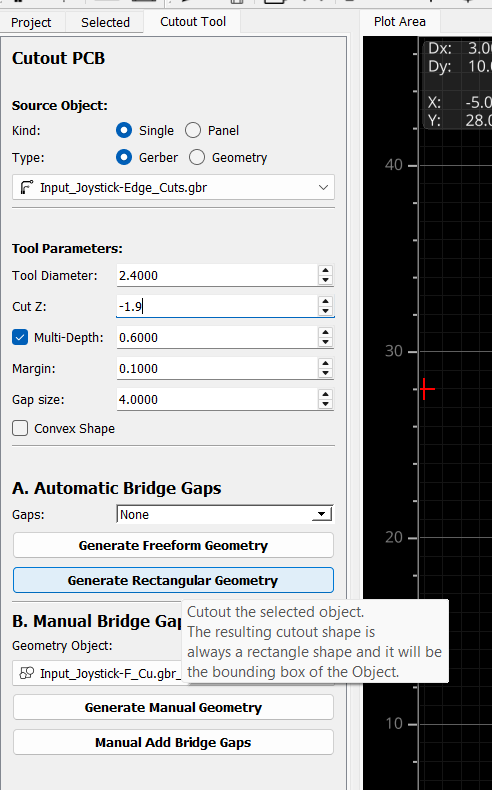
After double-clicking the Gerber object in FlatCAM, I entered the 'Cutout Tool' section to generate the rectangle geometry for the PCB outline. In this step, I set the required tool parameters and margins, ensuring the generated cutout path aligned precisely with the PCB's edge for accurate board milling
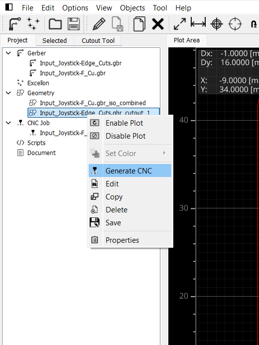
hen, I generated the CNC code from the defined cutout geometry. This code contains all the necessary instructions for the CNC milling machine, including toolpaths, spindle speed, and movement commands.
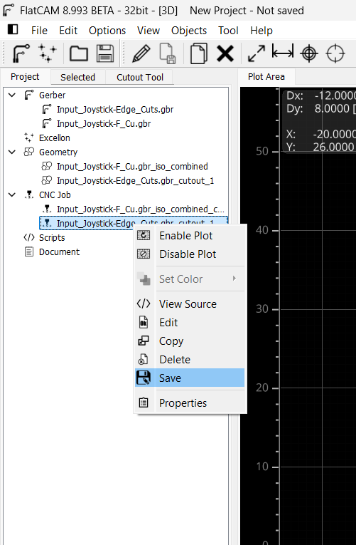
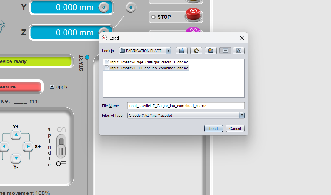
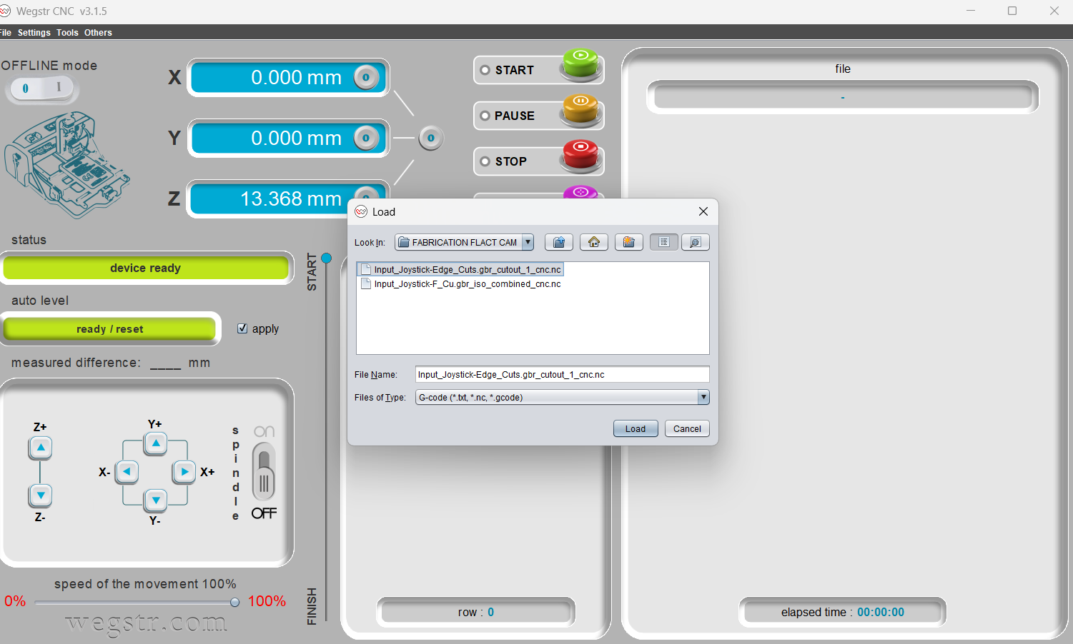
After generating the CNC code, I saved the CNC job file carefully. This saved file contains all the detailed instructions required for the CNC machine to accurately mill the PCB. Keeping the CNC job saved allows for easy retrieval and use during the actual fabrication process.
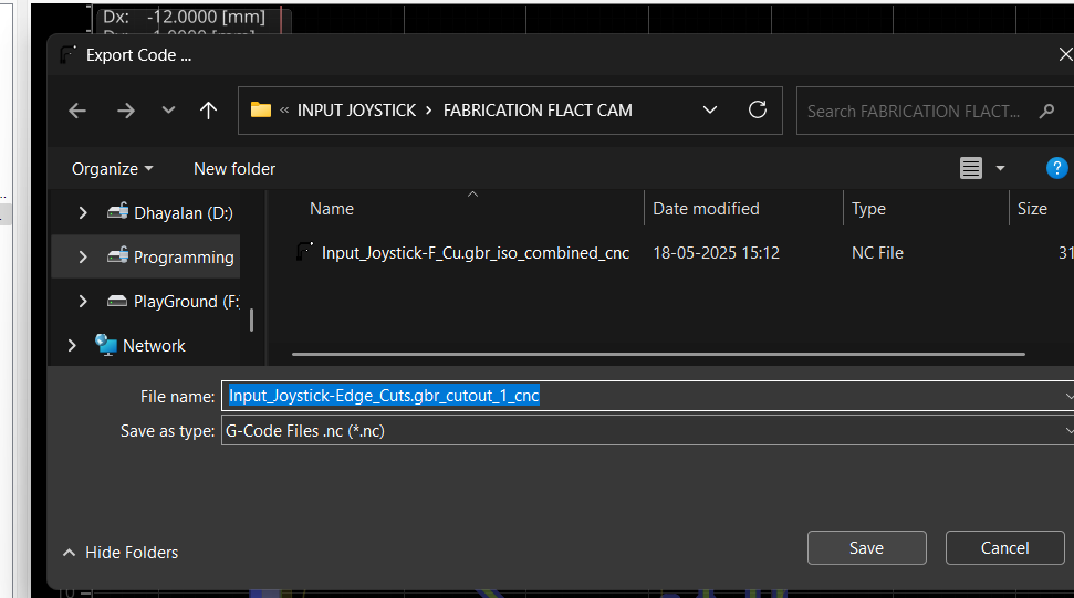
After saving the CNC job, I chose a convenient location on my computer to store the file. This organization helps me quickly access the CNC instructions later during fabrication
For the front copper layer (F.Cu), I followed a similar process. After generating the CNC job for the F.Cu toolpath, I saved it to a convenient location on my computer.
PCB milling involves mechanically removing material from a copper-clad board to create electrical isolation and form circuit patterns. Unlike traditional etching methods, which use chemical solutions to dissolve unwanted copper, milling uses precision-controlled milling bits to physically carve out the desired traces. The process is typically carried out using a Computer Numerical Control (CNC) milling machine, which is programmed to follow a specific design layout to guarantee accuracy and repeatability.
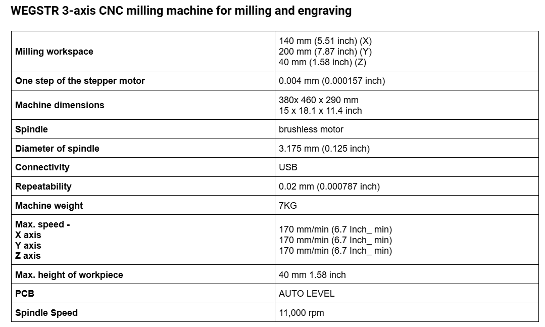
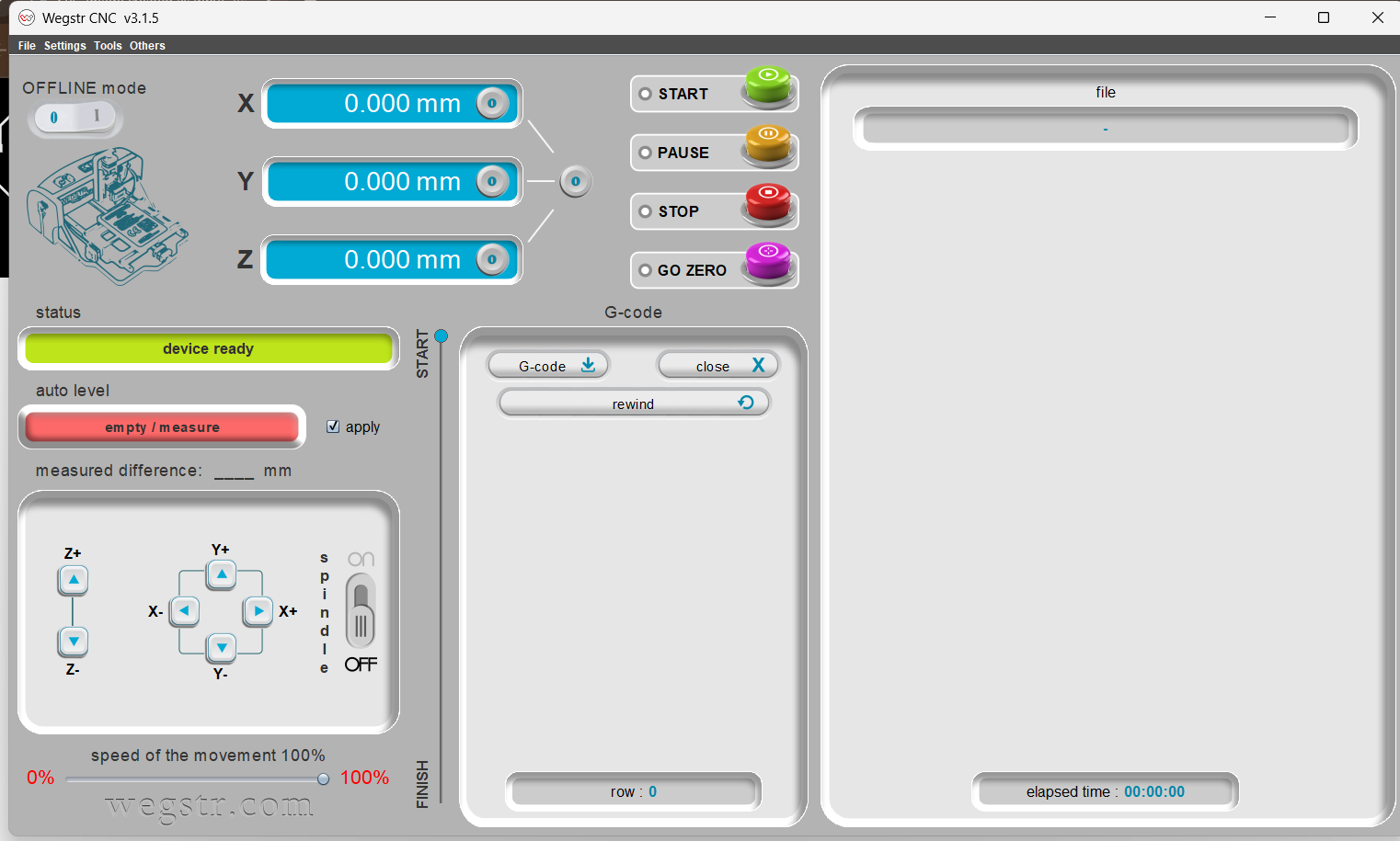
The Wegstr PCB milling machine is a compact desktop CNC designed specifically for rapid PCB prototyping. It allows users to fabricate circuit boards by milling copper-clad boards instead of traditional chemical etching. This is ideal for makers, engineers, and students who want to quickly test their circuit designs. The Wegstr software complements the machine by providing an intuitive interface to load, simulate, and control the CNC toolpaths (usually in G-code format). Users can import files generated from FlatCAM (like the front copper and edge cuts), visualize the milling process, set spindle speeds, and control axis movements with precision. Together, the Wegstr machine and software offer a clean, fast, and eco-friendly approach to producing custom PCBs directly from your digital designs.
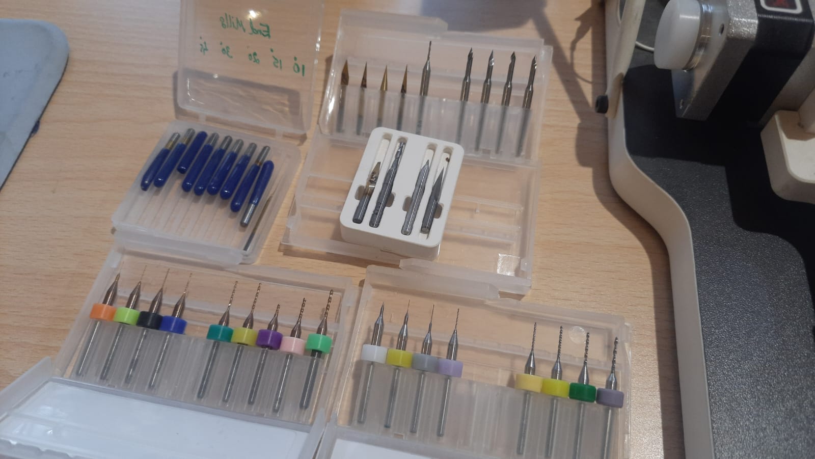
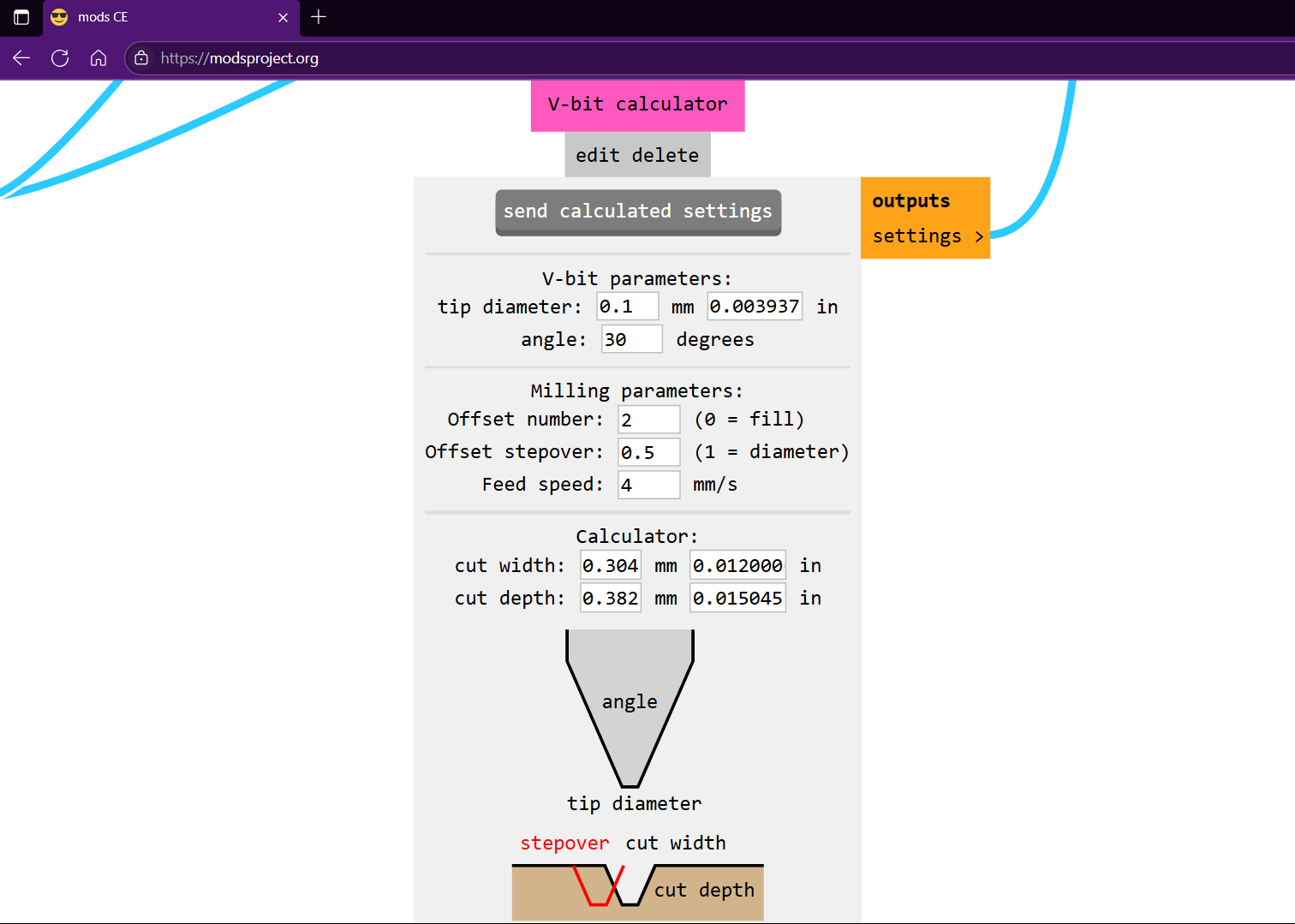
PCB milling bits are precision cutting tools used in CNC milling machines to engrave, cut, and drill printed circuit boards (PCBs). These bits come in various shapes and sizes, each designed for specific operations like trace isolation, hole drilling, or edge cutting. Common types include engraving bits, V-bits, and end mills.
Engraving Bits: Used for isolating copper traces.
End Mills: Ideal for drilling and cutting board outlines.
V-Bits: Provide sharp and clean traces for finer details.
Material is usually tungsten carbide for durability. Bit selection depends on trace width, depth, board material, and required precision.
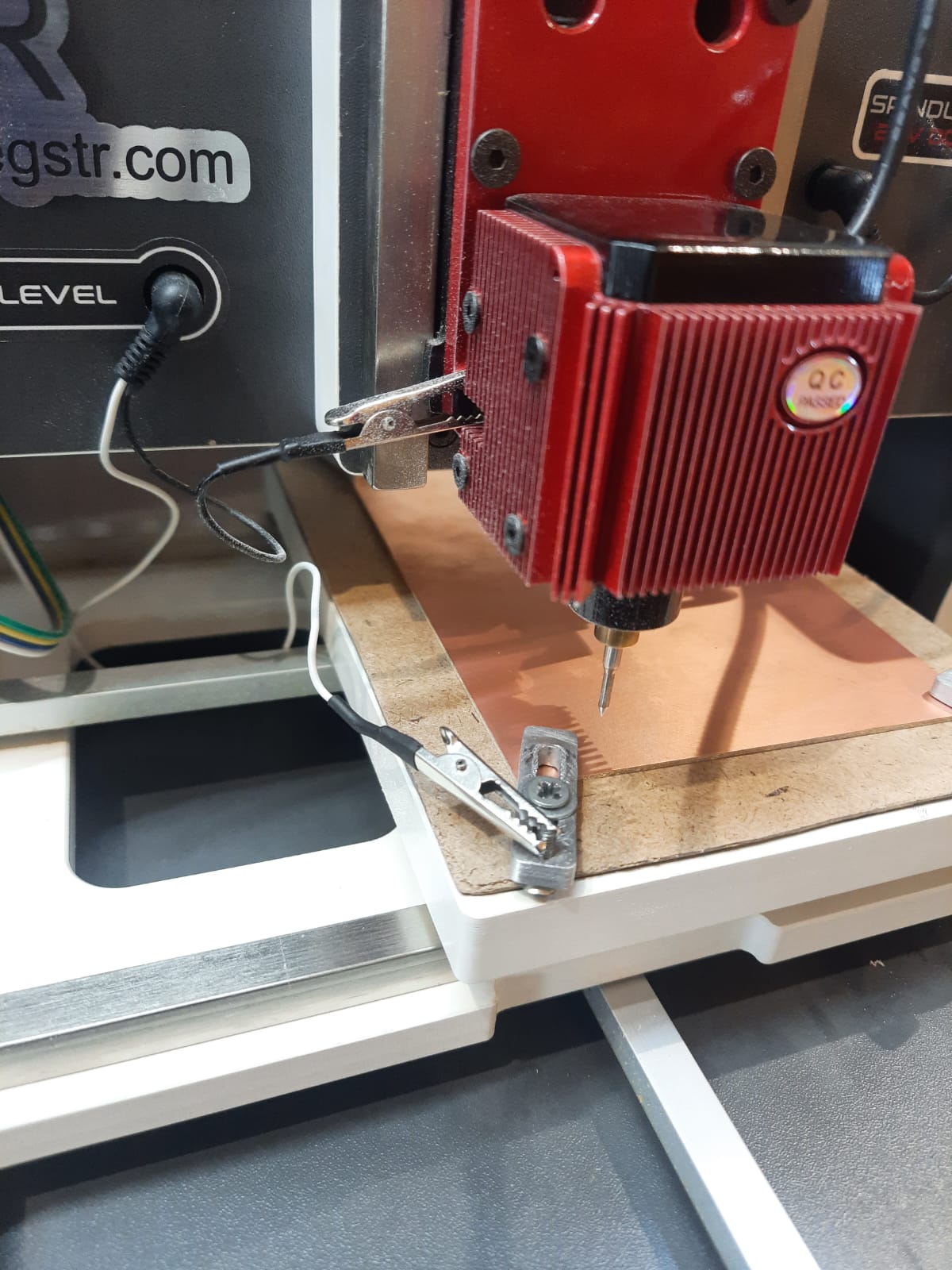
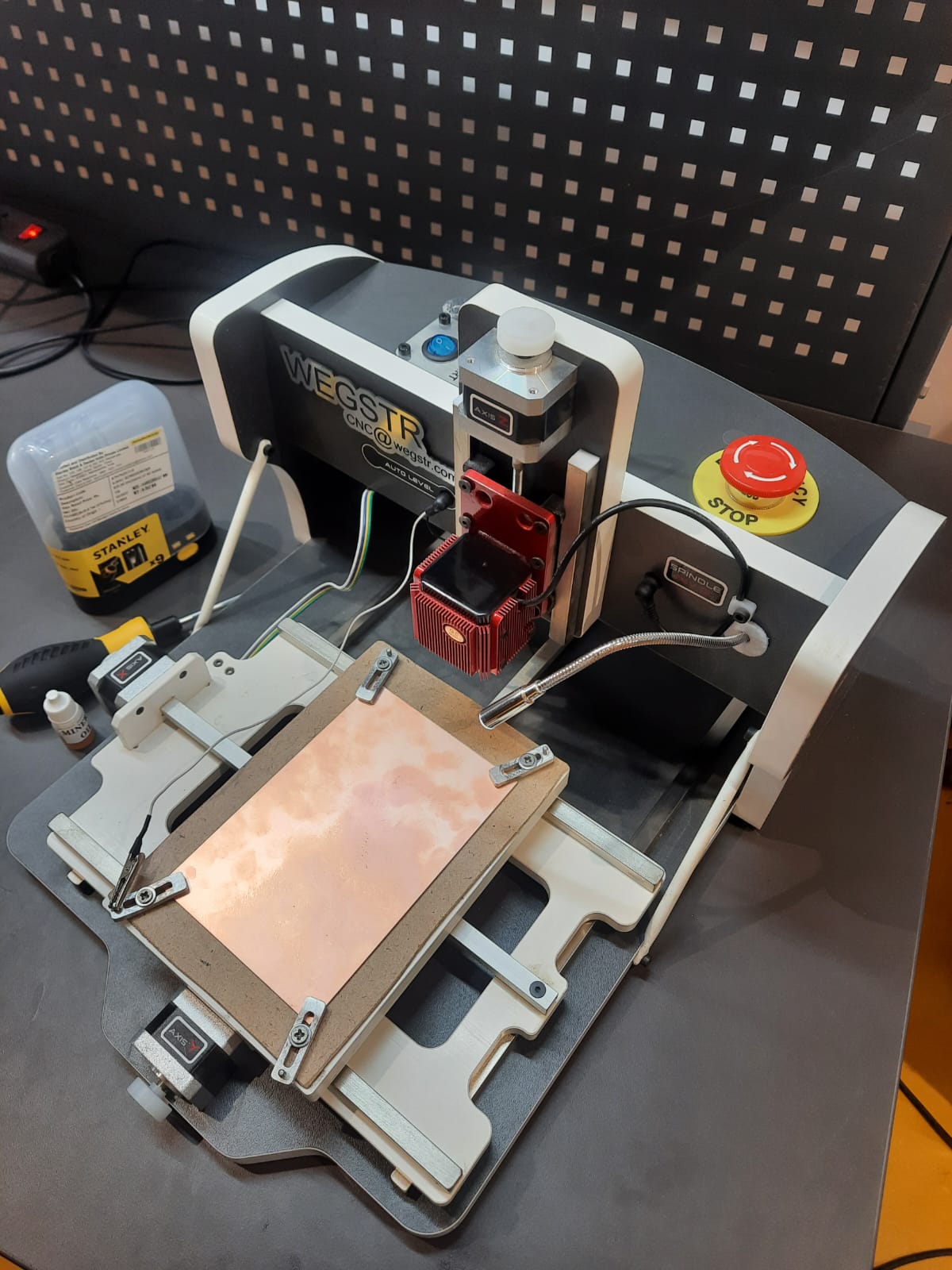
I connected the PCB milling machine to the PC and prepared it for fabrication. I securely fixed the copper-clad board onto the machine's bed using proper fixtures to ensure stability during milling. This alignment is crucial to prevent shifting, ensuring accurate cutting and precise trace isolation throughout the milling process.
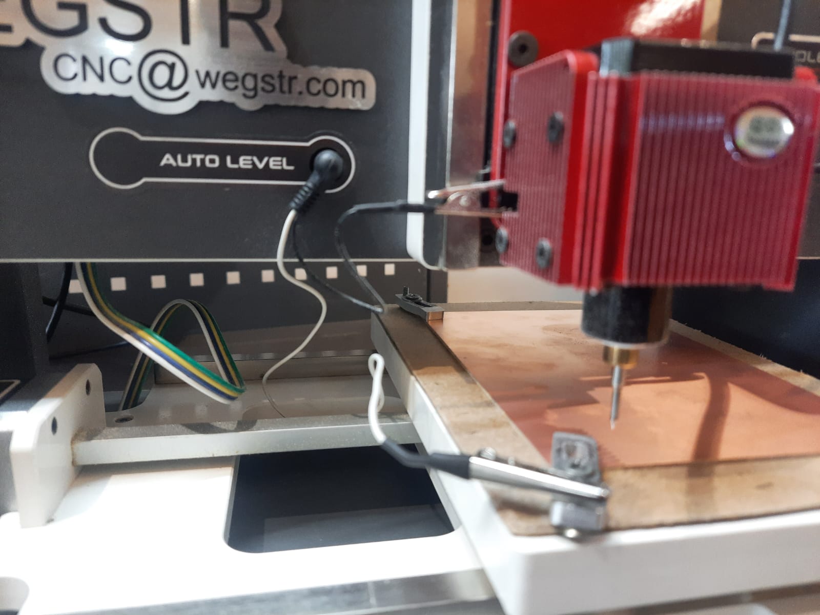
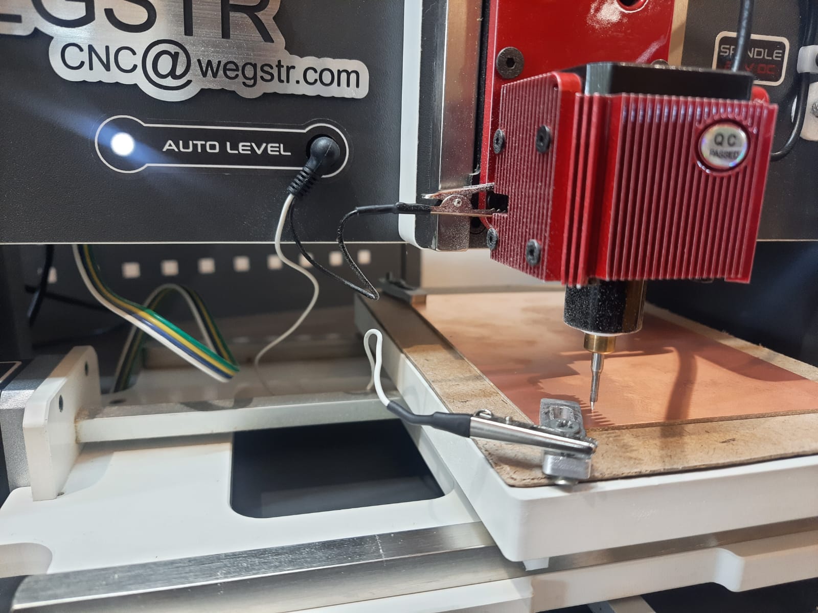
I manually verified the auto-leveling of the machine to ensure the milling bit would maintain accurate depth across the PCB surface. I carefully set the Z-axis zero position by gently lowering the bit until it just touched the copper surface, ensuring precise engraving during the PCB fabrication process.
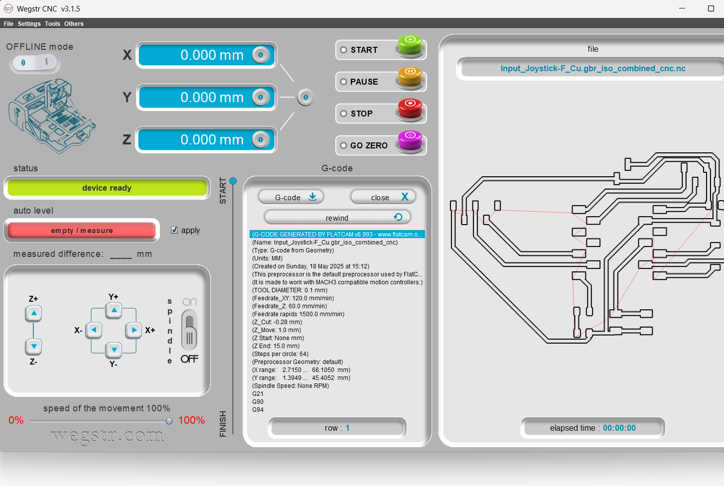
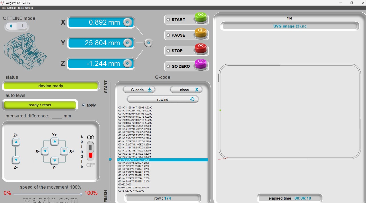
Then, I imported the F.Cu (front copper) file into the Wegstr software to verify auto-leveling across all test points. This step ensures the copper surface is uniformly leveled and aligned with the toolpath, preventing uneven milling and improving the accuracy and quality of the PCB engraving during fabrication.
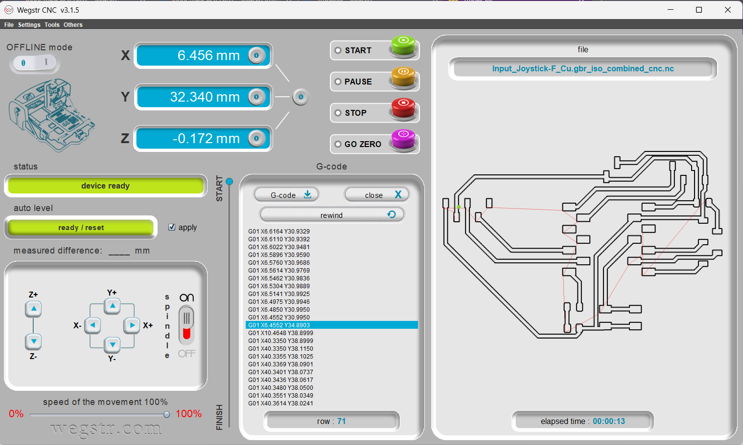
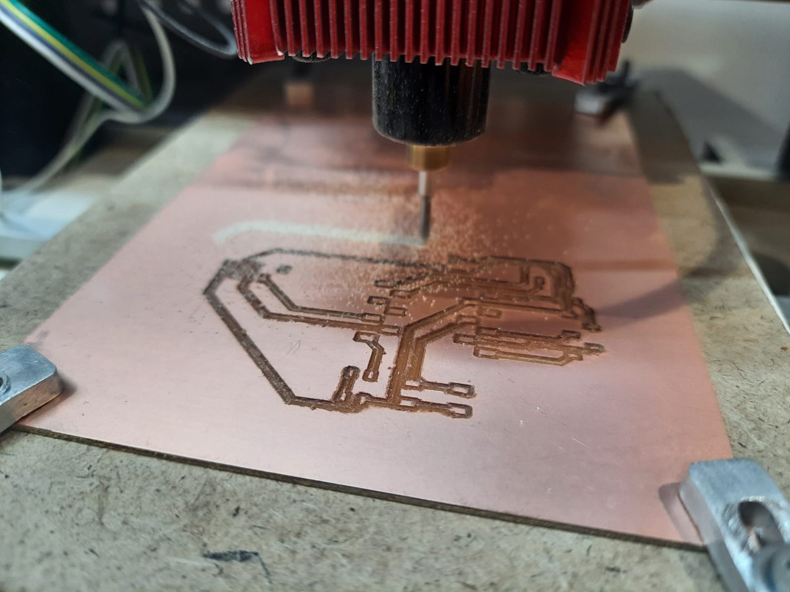
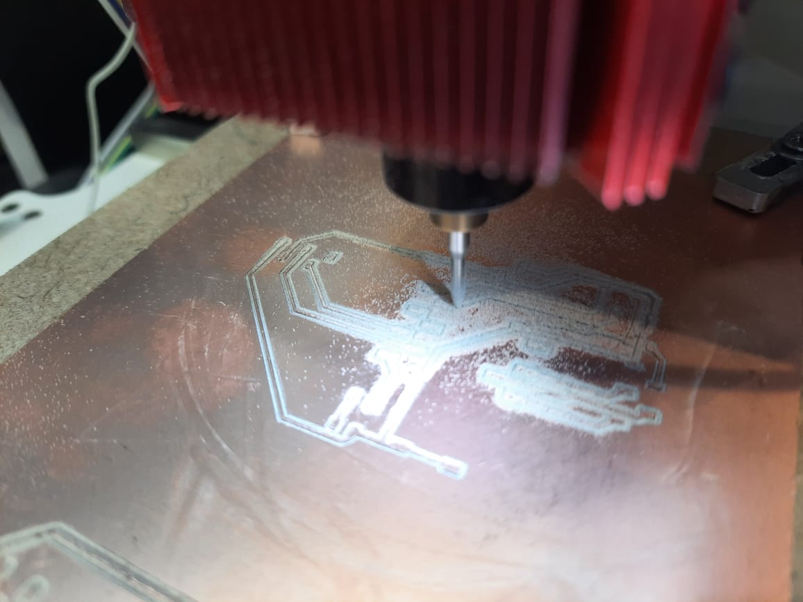
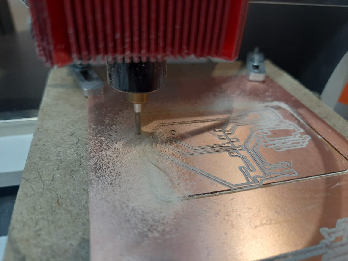
After completing the auto-leveling process, I initiated the milling operations on the Wegstr machine. The spindle followed the adjusted toolpaths based on the auto-leveled surface, ensuring precise cuts for the front copper traces
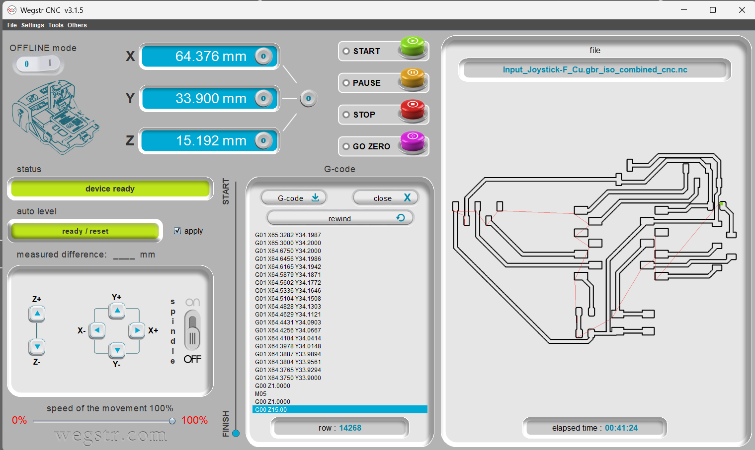
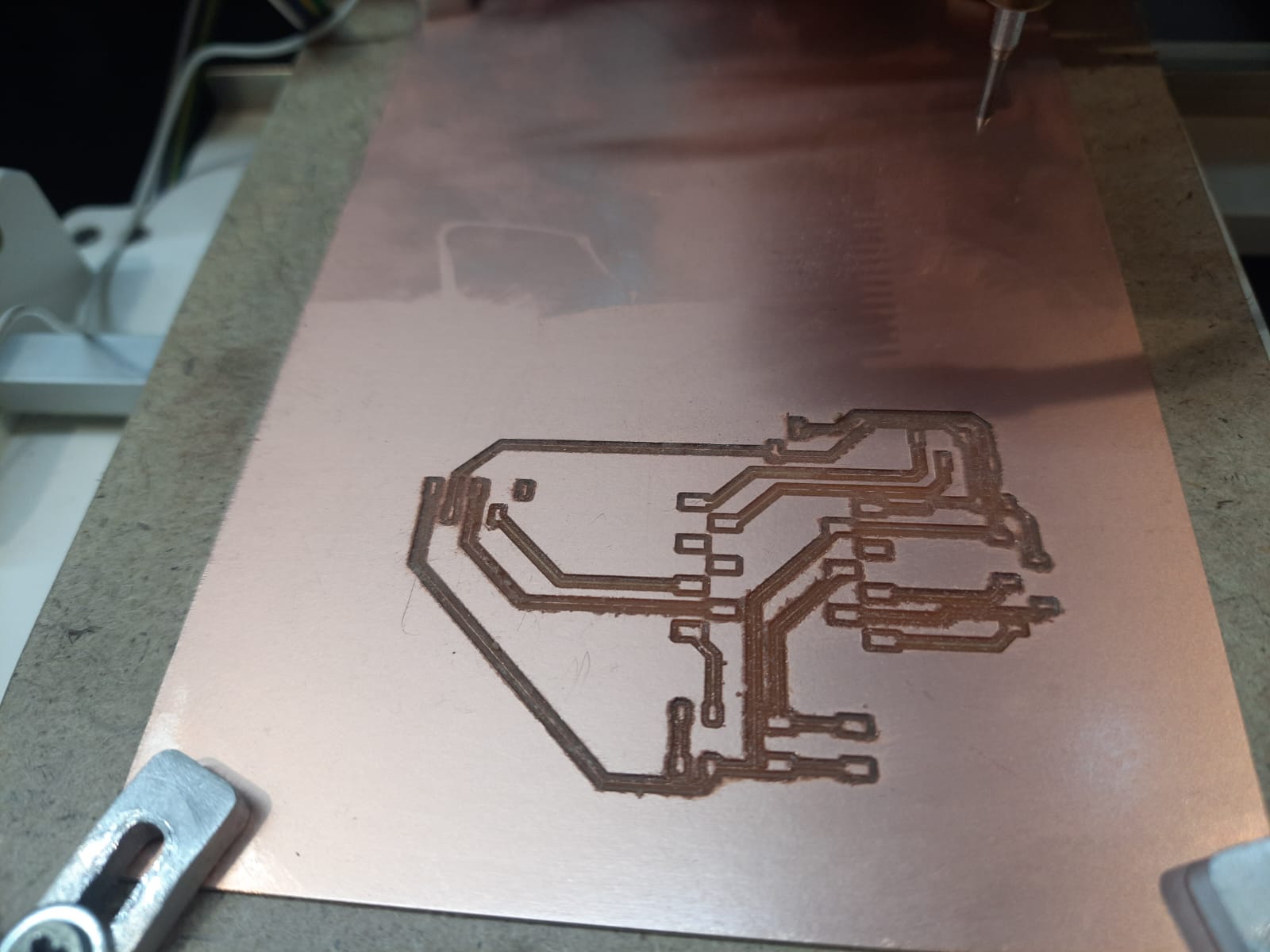
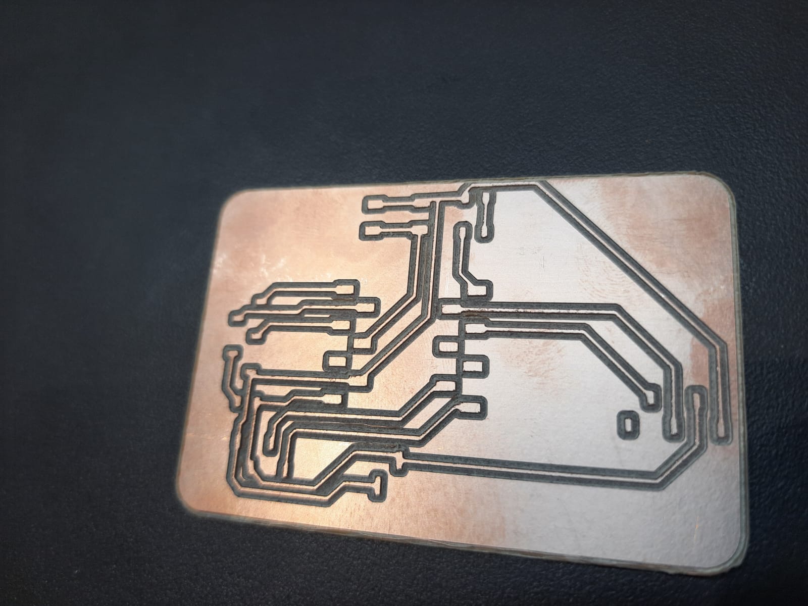
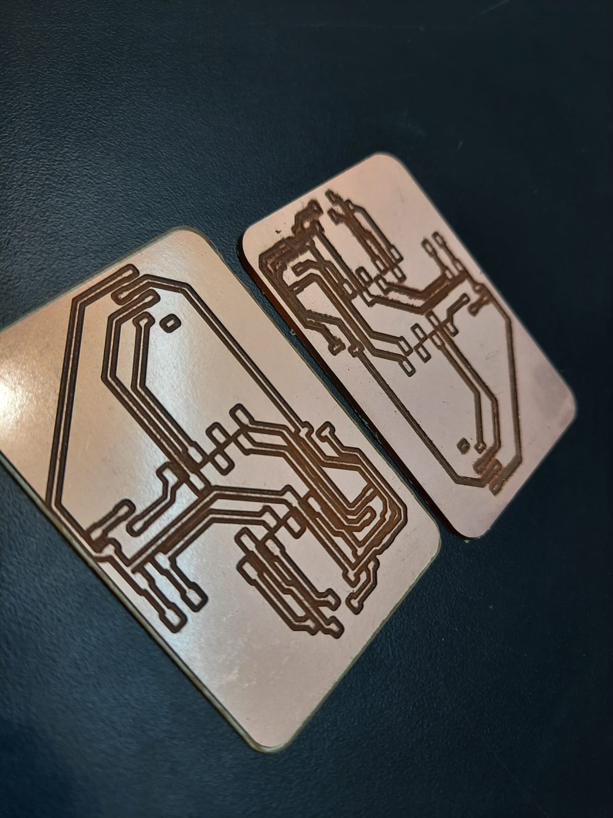
During the milling operation, the spindle rotated at 11,000 RPM, while simultaneously moving along the X and Y axes as defined by the NC (Numerical Control) code. The software automatically indicated completion once the milling process finished. Above is the final milled PCB output, which reflects the successful execution of the toolpath instructions.
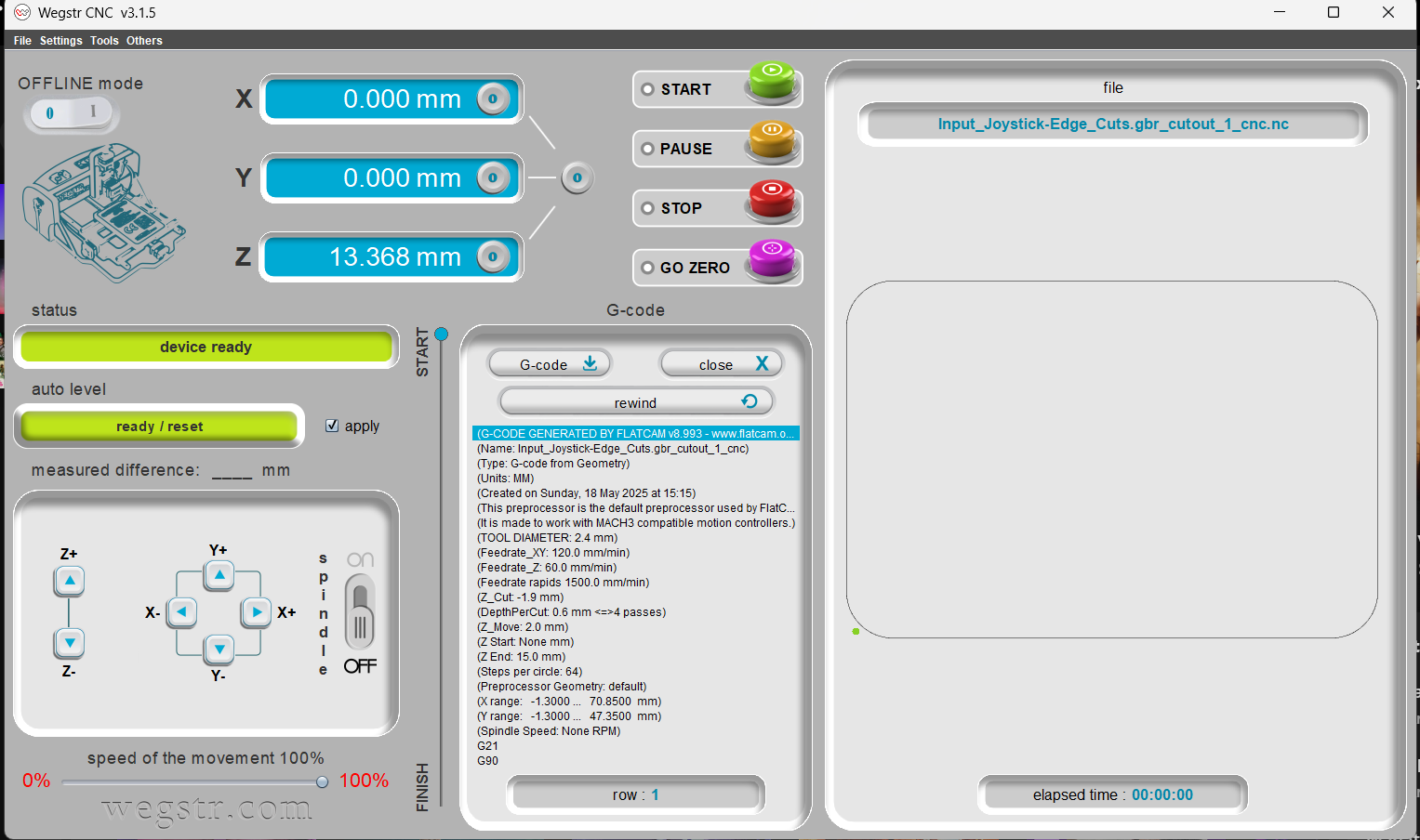
Then I imported the edge cut file into the Wegstr software. After importing, I verified the file using the preview option to ensure proper alignment and toolpath accuracy. Once confirmed, I proceeded to start the edge cutting operation, allowing the machine to cut out the PCB board outline precisely based on the design.
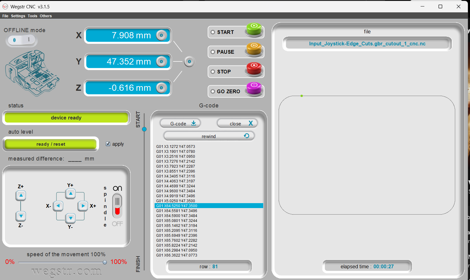
The machine completed the edge cut milling, but the result did not come out properly. Possible issues could include:
Incorrect cut depth settings.
Tool wear or damage (e.g., dull end mill).
Improper workpiece fixture, causing movement during milling.
Z-axis zeroing error, leading to shallow or uneven cuts.
MODS CE (Modular Object Design Software – Community Edition) is a browser-based software used primarily for controlling digital fabrication machines like PCB milling machines and lasers. It allows users to generate and send toolpaths directly to machines using modular workflows. Each module in MODS performs specific functions like file import, toolpath generation, coordinate transformation, and machine communication. MODS CE is widely used in Fab Labs and educational environments due to its flexibility, real-time control, and support for SRM-20, Modela, and other Roland machines.

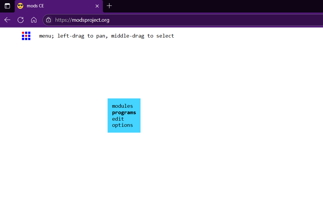
In MODS CE, to begin using a specific workflow:
Right-click anywhere on the workspace and go to:
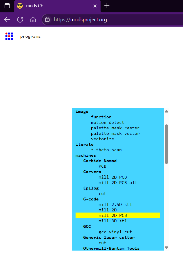
Programs → choose the required module chain (e.g., "PCB milling – Roland SRM-20", "G-code sender", or "Image to G-code").
This action loads a predefined flow of modules, such as:
Read file (Gerber or PNG)
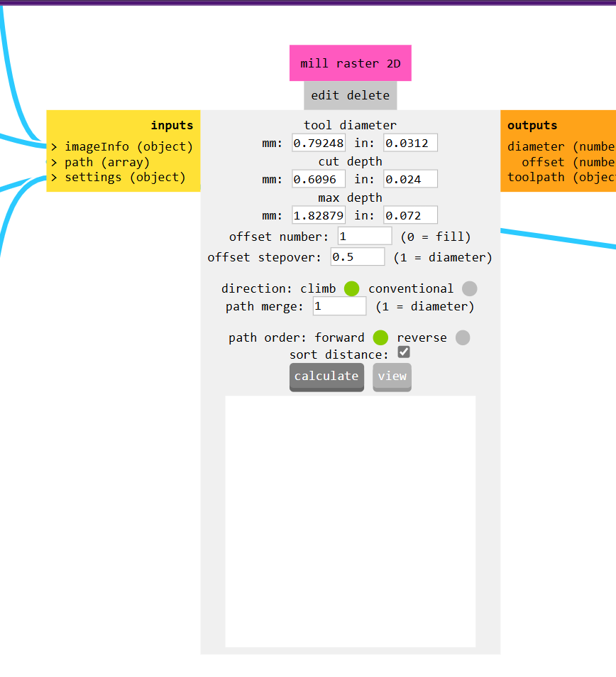
Mill raster 2D (for toolpath generation)
WebSocket device (for machine communication)
You can then customize the parameters, generate toolpaths, and send them to the machine for fabrication.
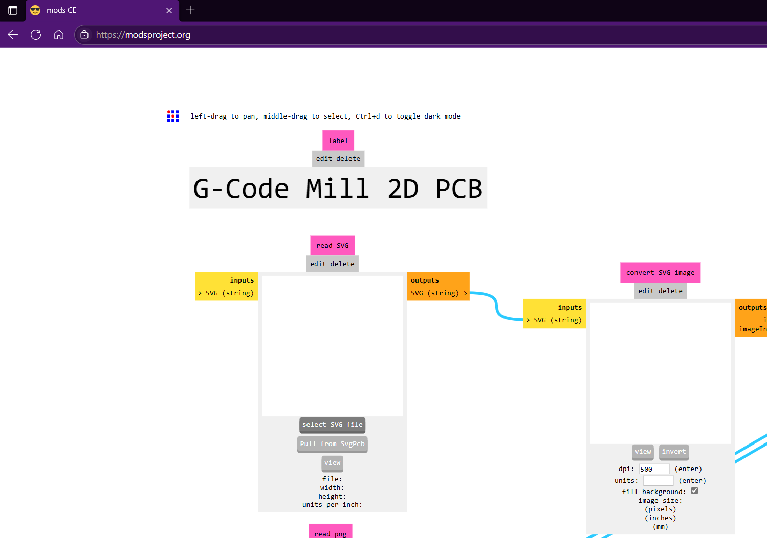
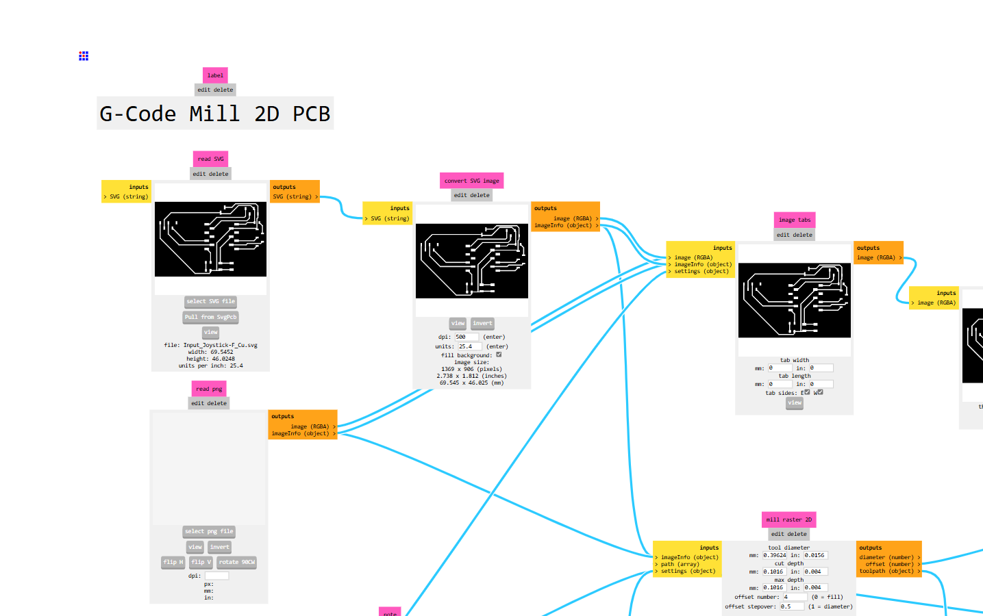
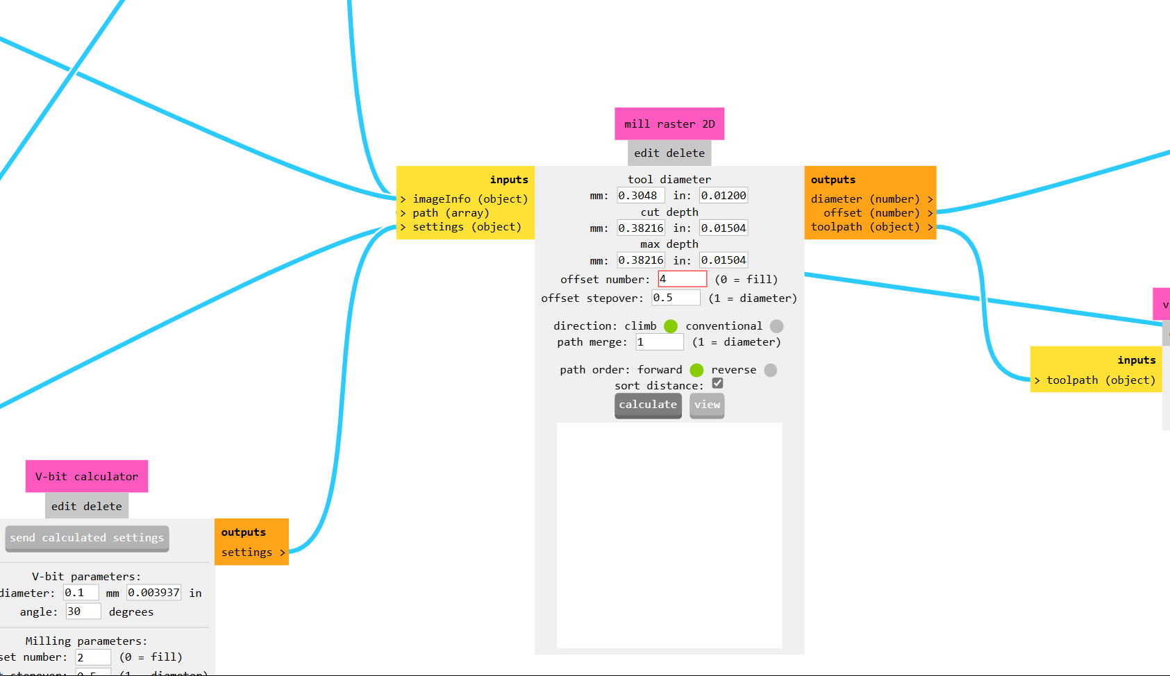
In MODS CE, under the mill raster 2D module, you can adjust the milling path spacing to ensure there's enough clearance between traces for placing components:
Change the “offset number” parameter from the default (usually 2) to 4.
This increases the number of tool offset passes, widening the isolation gap between copper traces. It helps in:
Reducing the chance of shorts
Making room for component pads
Improving soldering accessibility
Always preview the toolpaths after changing this to verify the proper spacing before sending to the machine
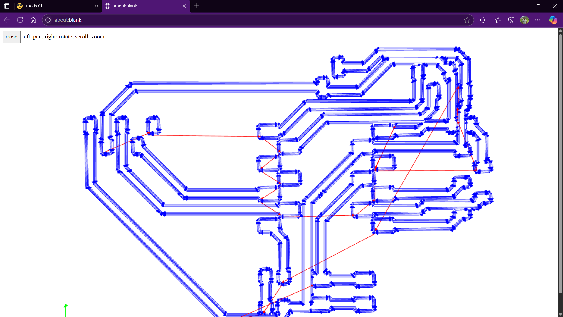
After setting the offset number in MODS CE, the next step is to preview and verify the toolpath:
Click “calculate” to generate the updated milling paths.
Use the “view toolpath” or “display path” module to see the actual tool movement.
Carefully inspect:
Trace isolation width
Component pad clearance
Tool entry and exit points
Verifying the toolpath helps ensure your design is correctly interpreted and ready for fabrication without risking damage to the board or incomplete milling.
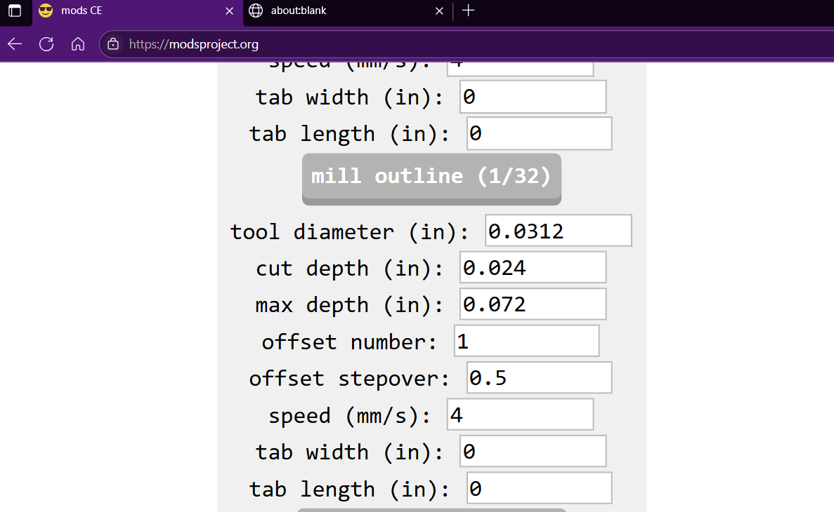
For the edge cut operation in MODS CE, I selected the “mill outline” option, set the tool overlap to 0.4 mm for smooth cutting, and used the same settings in “mill raster 2D.” This ensured a precise and clean edge cut, readying the PCB for separation.
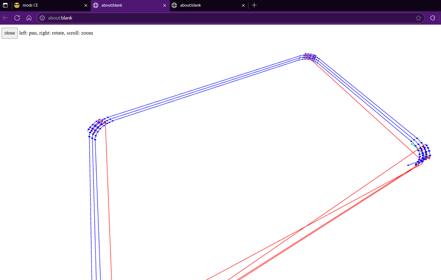
Preview of edge cut
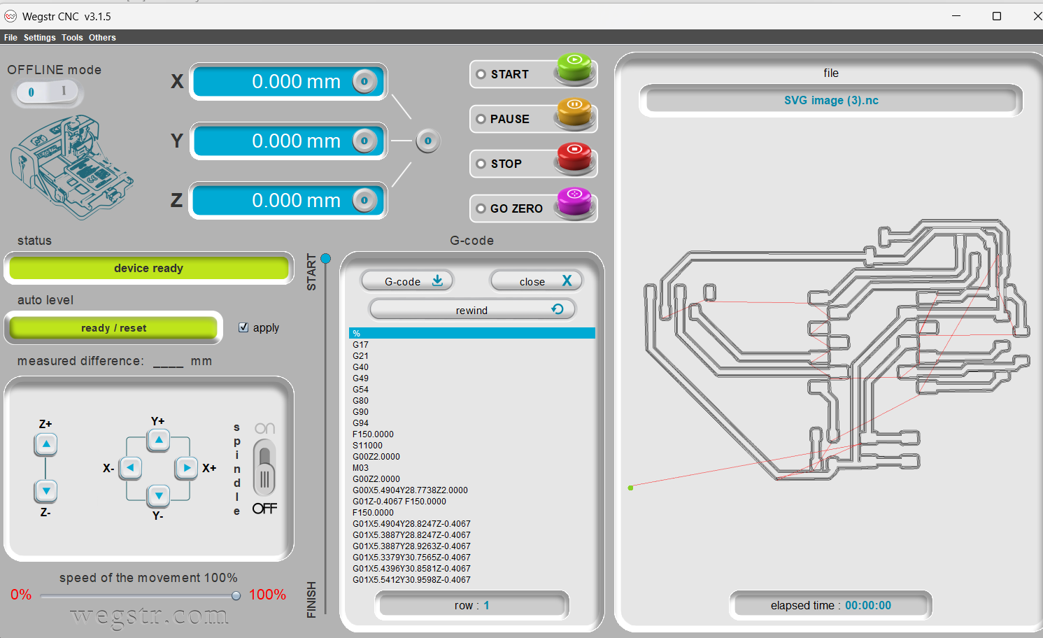
I imported the NC file and performed the auto-leveling test, just as in the previous milling operation. This step ensures the milling bit adjusts to the surface variations of the PCB, enabling accurate and consistent depth cutting during the fabrication process.
During milling Operation
Then, I imported the edge cut file into the Wegstr machine software and performed the required tasks. This included verifying the tool path, ensuring proper alignment, and starting the milling process to cut out the board outline accurately. The process helps finalize the PCB shape for component assembly.
Flat cam Output
mods ce Output
FlatCAM didn’t work well, so I’ve decided to proceed with Mods CE instead
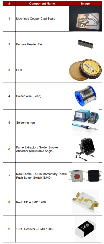
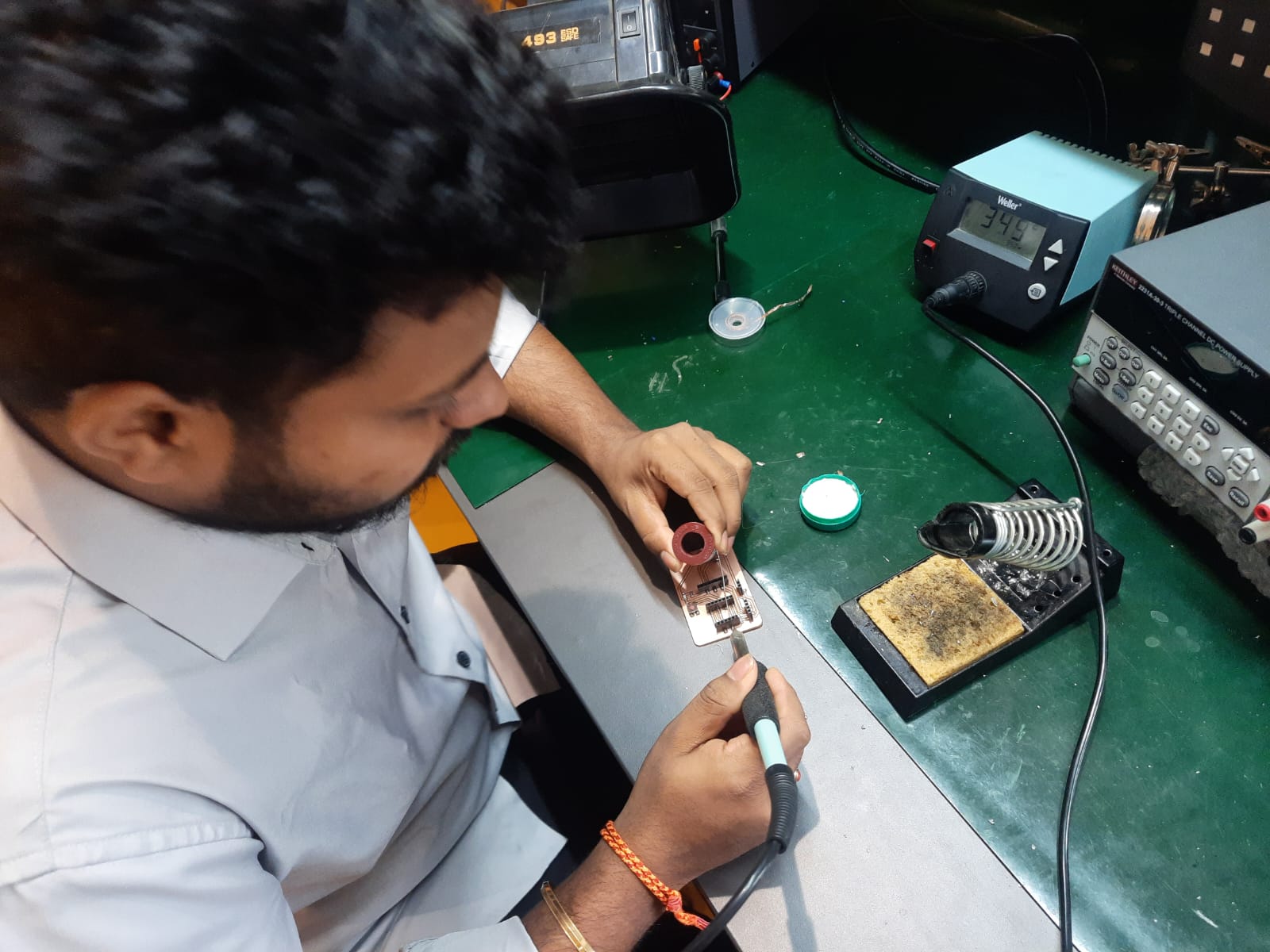
There are two main types of solder: lead-based and lead-free. Lead-based solder (usually a mixture of tin and lead) is easier to work with but is less environmentally friendly. Lead-free solder, often composed of tin, silver, and copper, is safer for users and more compliant with health regulations (like RoHS).
Basic tools for soldering include:
Soldering iron – heats the solder
Solder wire – the filler metal
Soldering stand – holds the iron when not in use
Sponge or brass wool – cleans the iron tip
Flux – helps solder flow better and prevents oxidation
Good soldering ensures reliable electrical connections. It requires practice, proper technique, and attention to heat, timing, and cleanliness.
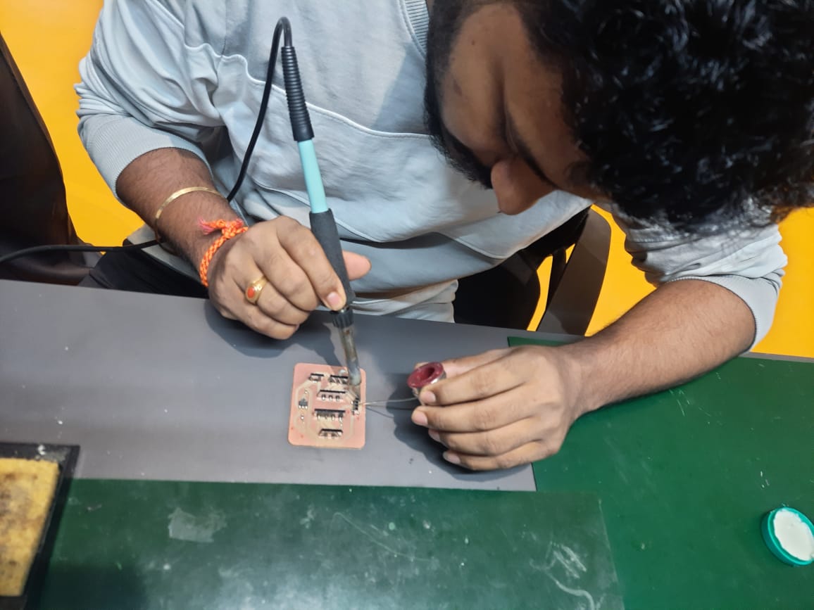
After connecting the components, the circuit didn’t work initially. Upon inspection, I discovered a broken copper track on the PCB. I repaired it by soldering a jumper wire across the break. Sometimes, this issue occurs due to the thin 1mm copper layer on PCB clad boards.
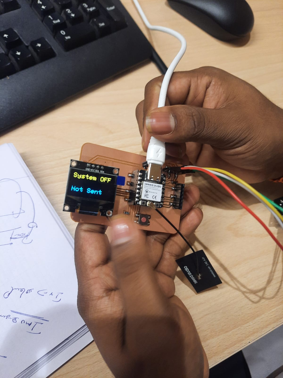
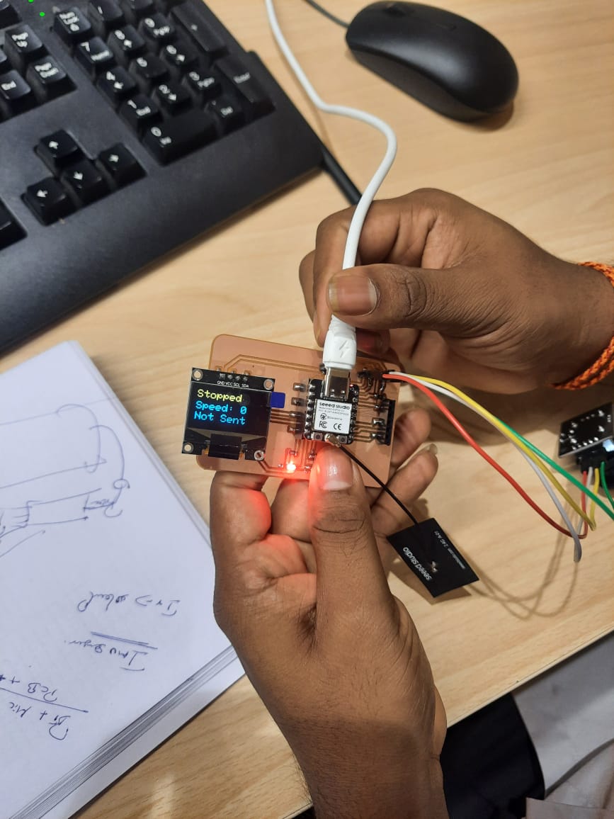
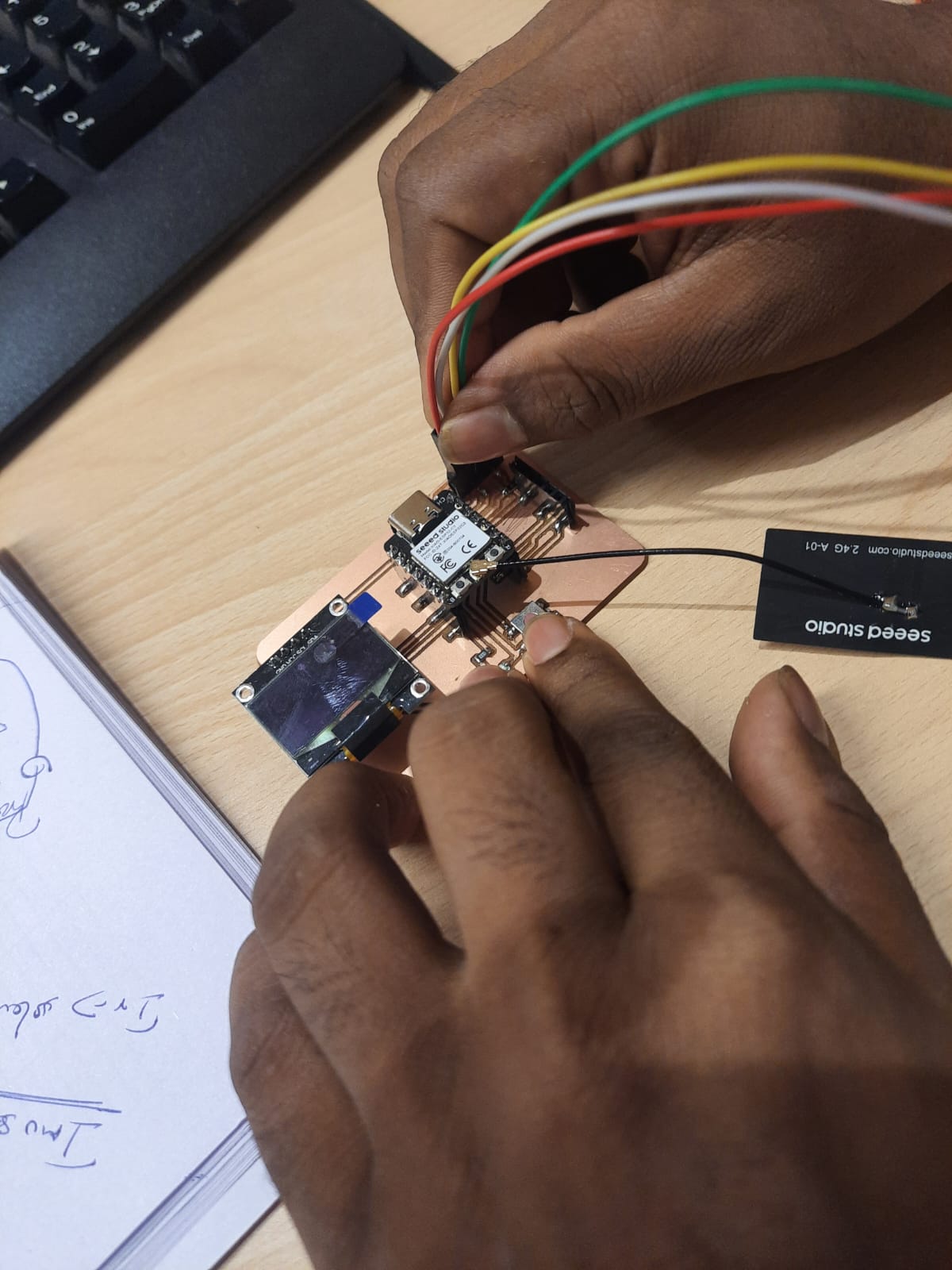
I programmed the board for the input device. Let's explore its functionality in the next week's assignment.the Text Element.