Group assignment
Individual assignments

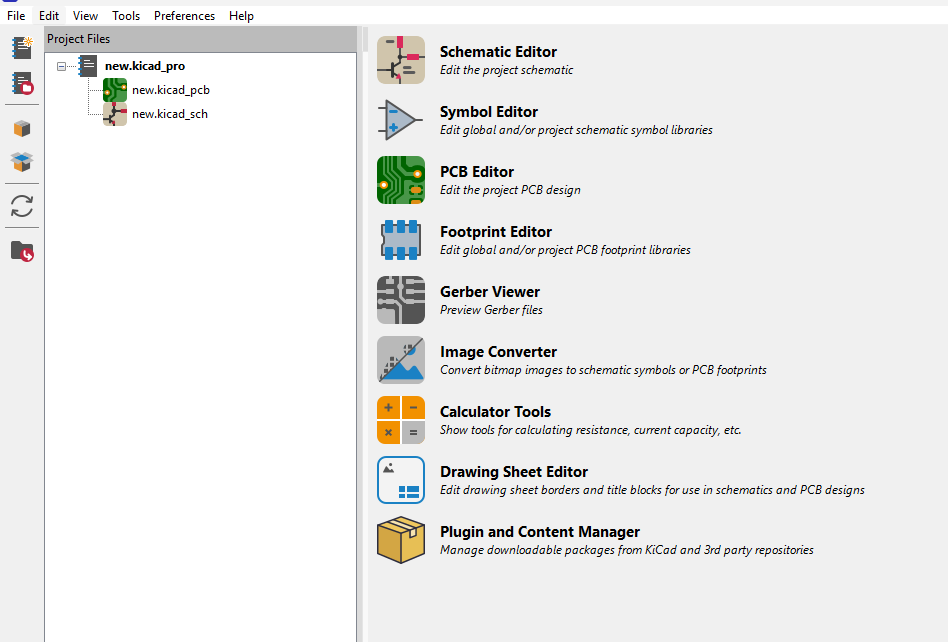
KiCad is a powerful, open-source software suite used for electronic design automation (EDA). It allows users to create schematic diagrams, design printed circuit boards (PCBs), and manage component libraries efficiently. With features like a 3D viewer, electrical and design rule checks (ERC/DRC), and Gerber file generation, KiCad is widely used by engineers, hobbyists, and product developers to bring electronic circuits from concept to reality. Its modular environment includes tools for schematic capture, PCB layout, footprint editing, and BOM generation.

Before starting the PCB design process in KiCad, it’s essential to install or include the necessary libraries. These libraries contain the symbols and footprints for various electronic components. Proper setup ensures accurate circuit design, component placement, and compatibility with fabrication tools later in the workflow
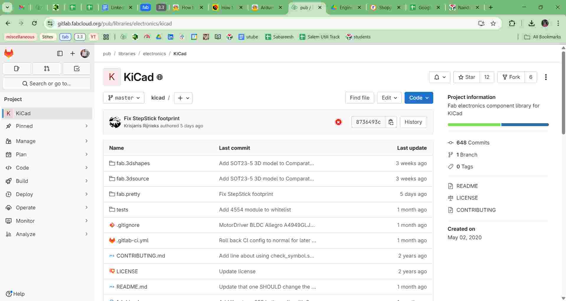
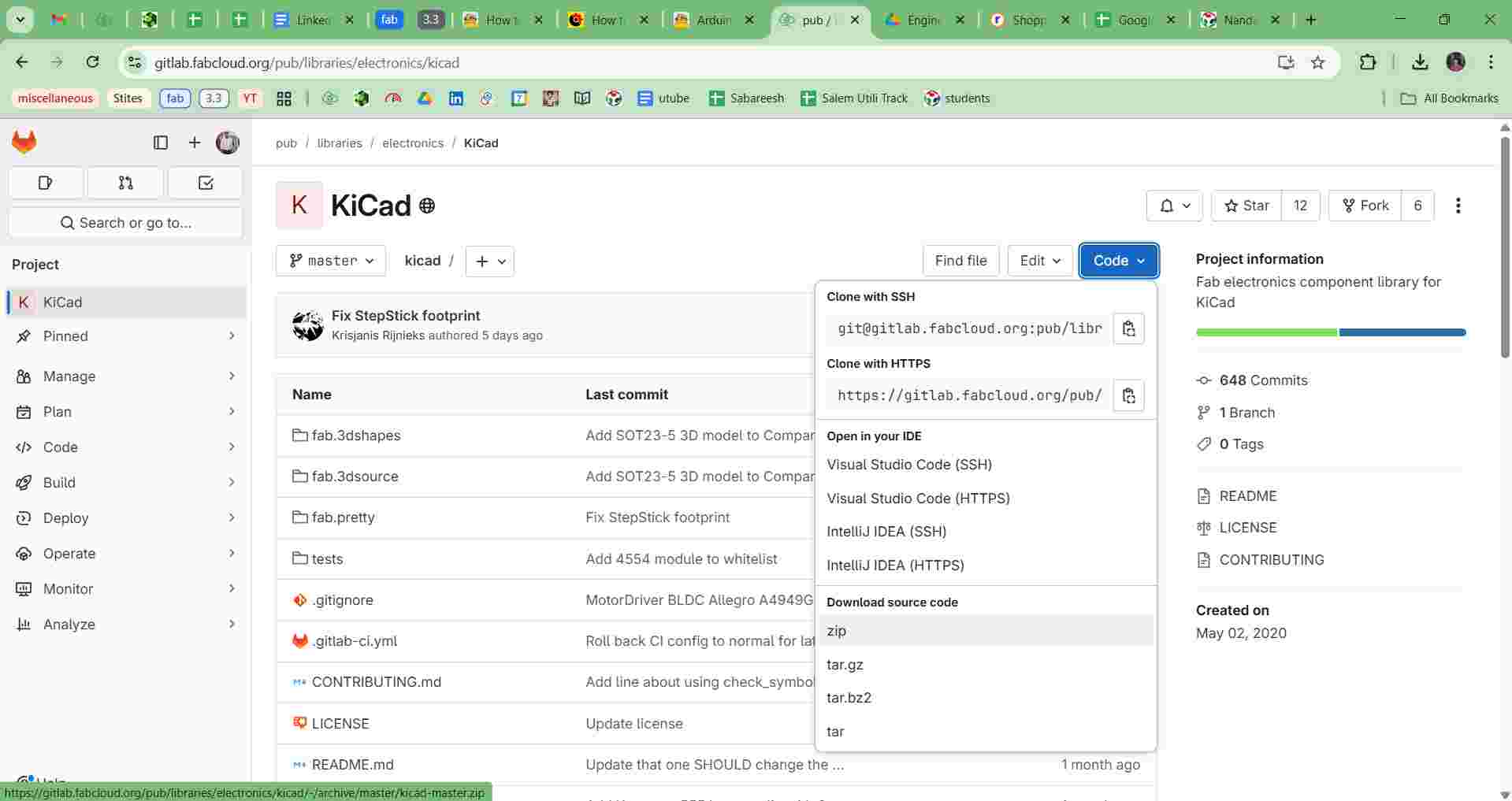
As part of the Fab Academy workflow, I downloaded the official Fab Academy KiCad library in ZIP format from the Fab Academy website. This library includes specific components and footprints commonly used in Fab Lab projects, making it essential for designing compatible and standardized electronic circuits.
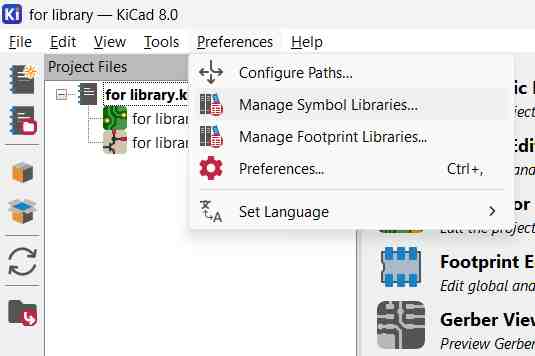
After opening KiCad, I navigated to the Preferences menu and selected “Manage Symbol Libraries.” This step is crucial for adding external libraries, such as the Fab Academy KiCad library, to ensure all the required component symbols are available while designing the schematic for my electronics project.
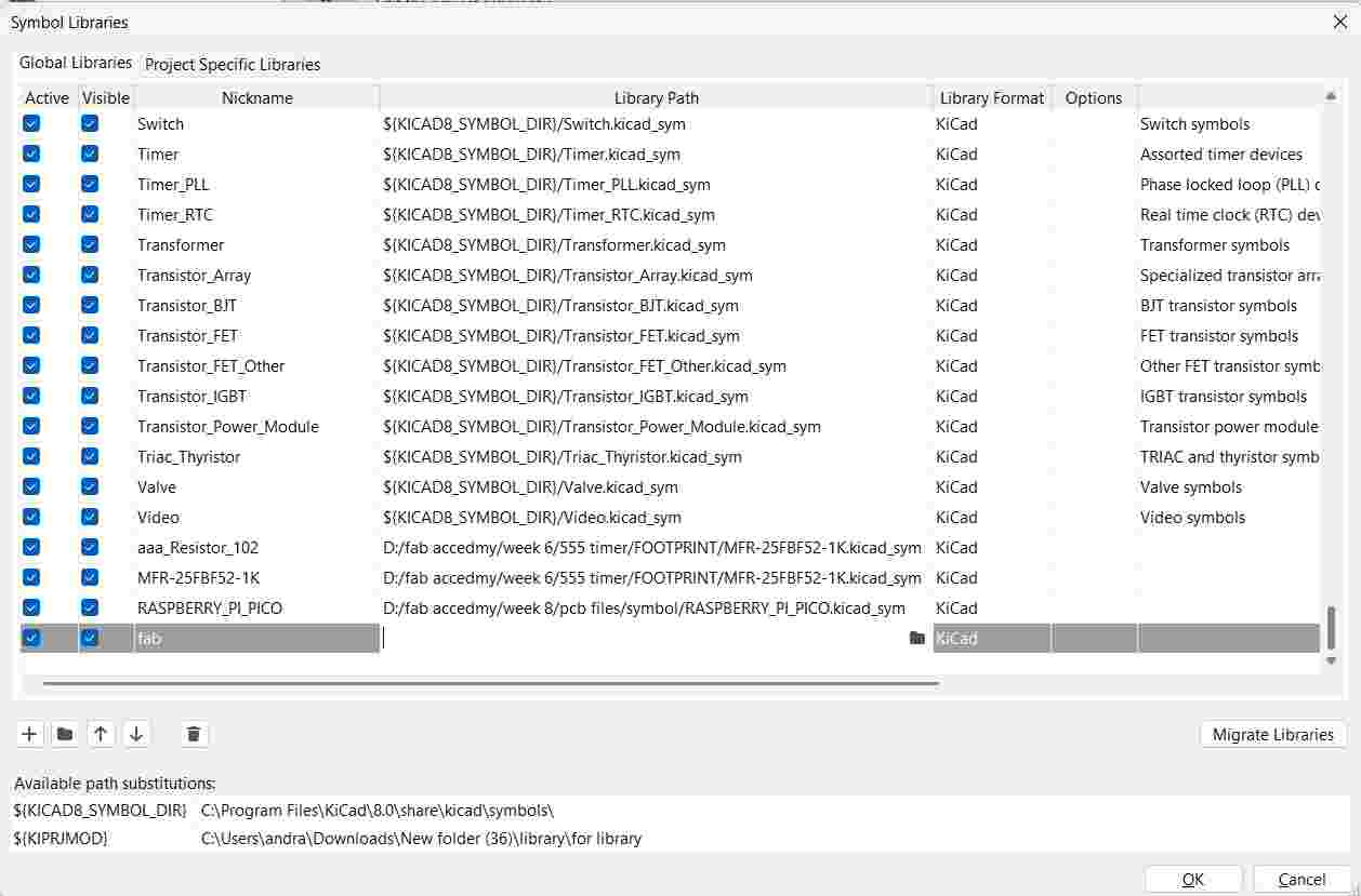
In the Manage Symbol Libraries window, I clicked the “Add” button to include a new library. I then entered a suitable library name, which helps identify the added library in the list. Naming it clearly (e.g., "FabAcademy_Lib") ensures easy access during schematic and PCB design work.
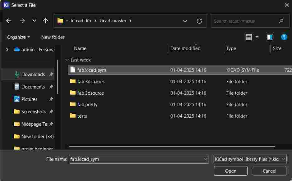
After naming the new library in KiCad, I navigated to the location where I extracted the Fab Academy KiCad library ZIP. I selected the appropriate .lib symbol file, which contains the component symbols needed for the schematic. This step made the custom components accessible in my design.
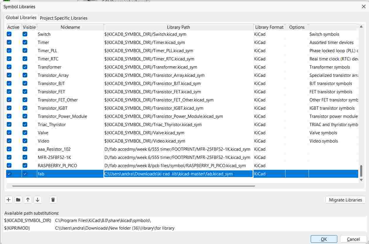
Once I selected the correct symbol file, I clicked OK to confirm and complete the library setup process. The newly added Fab Academy library was now successfully integrated into KiCad, allowing me to access and use all the required component symbols in my circuit schematic design.
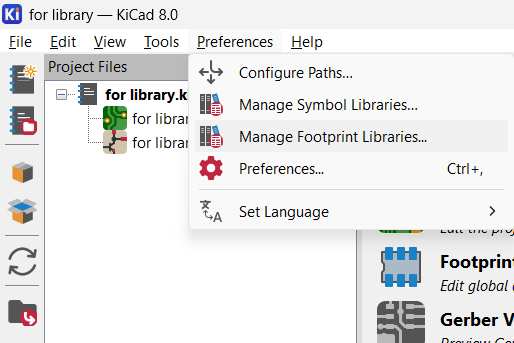
To link the physical component footprints for PCB layout, I went to Preferences > Manage Footprint Libraries in KiCad. This section allows me to import custom .pretty footprint libraries, ensuring that each component in my schematic has an accurate physical representation for the PCB design process.
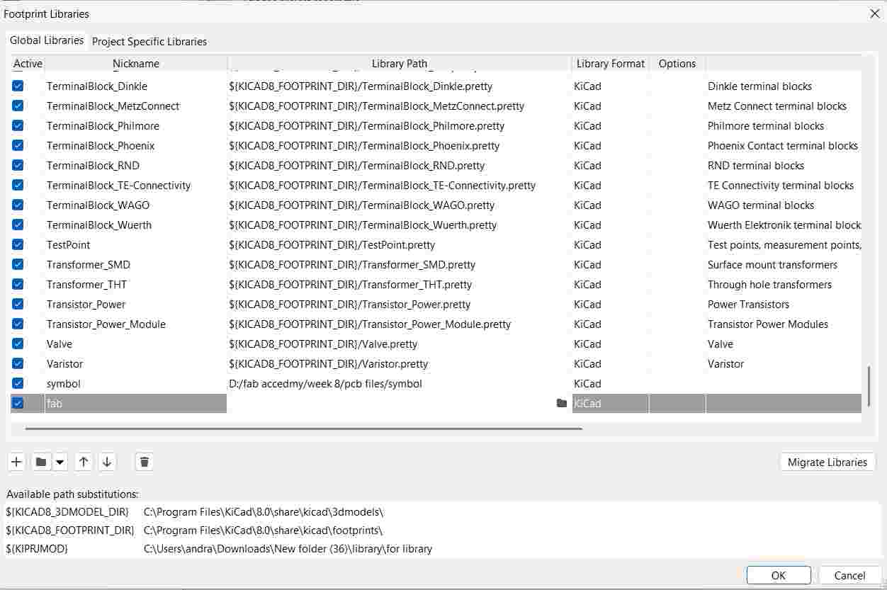
In the Manage Footprint Libraries window, I clicked “Add” and entered a suitable library name to represent the footprint collection, such as FabAcademy_Footprints. This name helps organize and identify the library during PCB layout, making it easier to assign the correct footprint to each component.
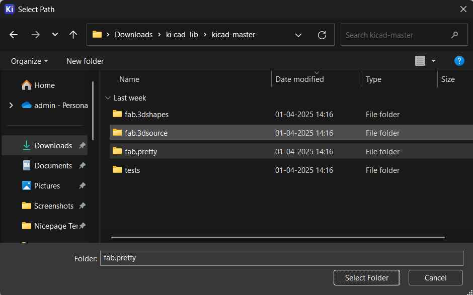
After naming the footprint library, I browsed to the location where I had extracted the Fab Academy KiCad footprint library. I then selected the appropriate .pretty folder, which contains all the footprint files. This enabled KiCad to recognize and use these footprints during PCB layout.
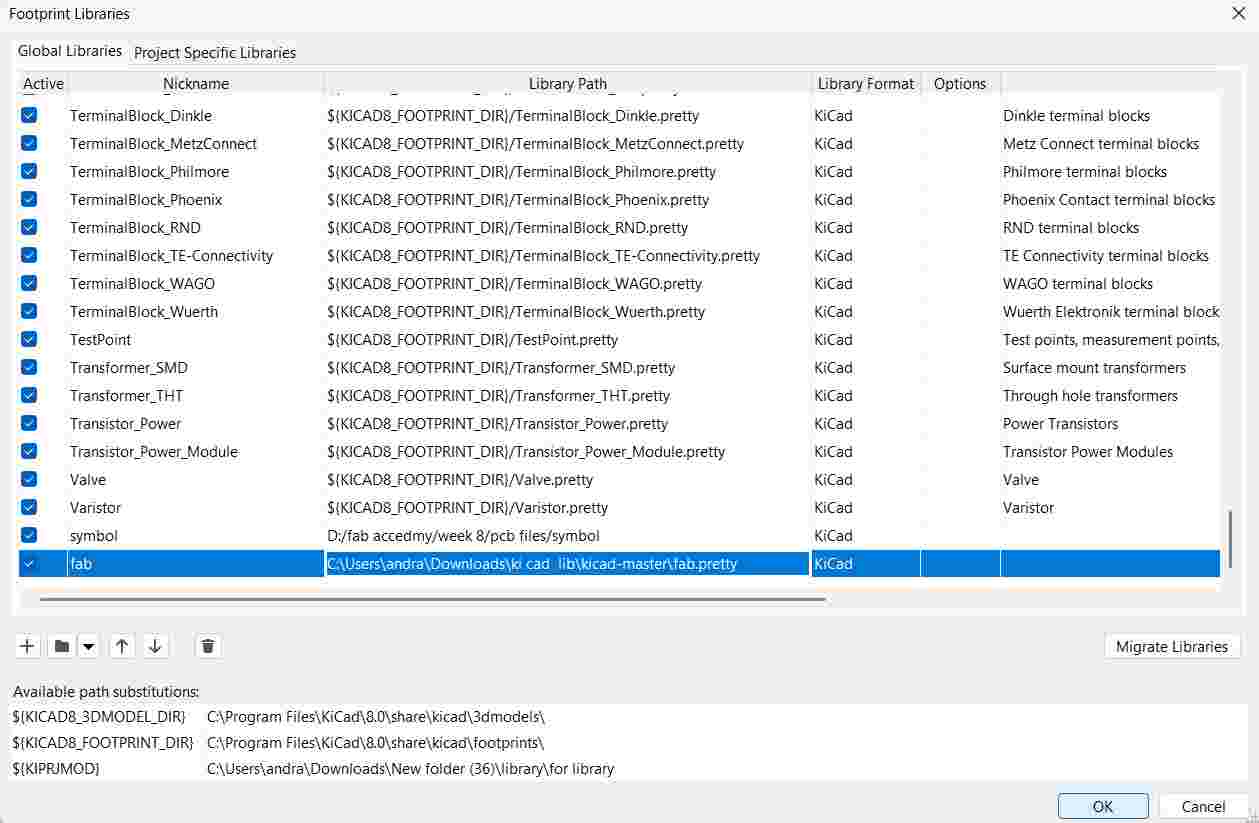
Once I selected the correct .pretty folder, I clicked OK to complete the import process. The Fab Academy footprint library was now successfully added to KiCad, allowing me to assign accurate physical footprints to each schematic component during the PCB design phase.
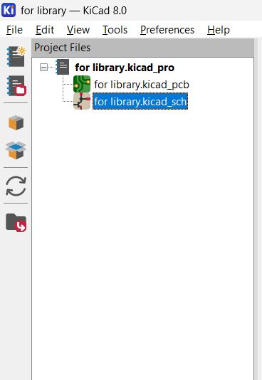
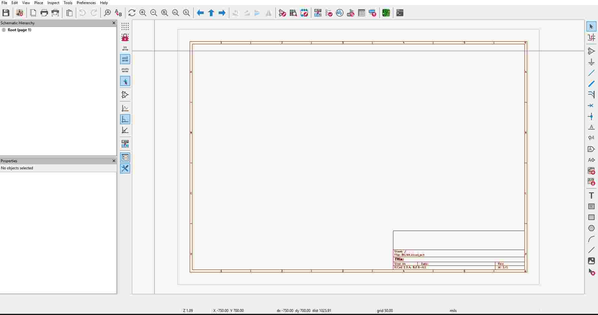
To verify that the symbol and footprint libraries were successfully imported, I created a new project in KiCad. I then opened the Schematic Editor to begin placing components. This step confirmed that the newly added Fab Academy libraries were properly loaded and accessible.
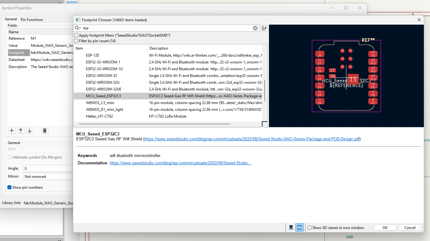
Inside the Schematic Editor, I used the “Add Symbol” tool, which can be quickly accessed by pressing the shortcut key "A". This feature allowed me to search for and place components from the imported libraries directly into my schematic for further circuit design and connection.
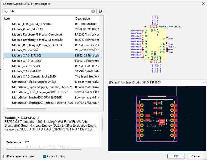
Using the Add Symbol tool in the Schematic Editor, I searched for and placed the Module_XIAO-ESP32C3 symbol from the imported Fab Academy library. This microcontroller module is the core of my project, and adding it to the schematic was the first step in building the circuit.
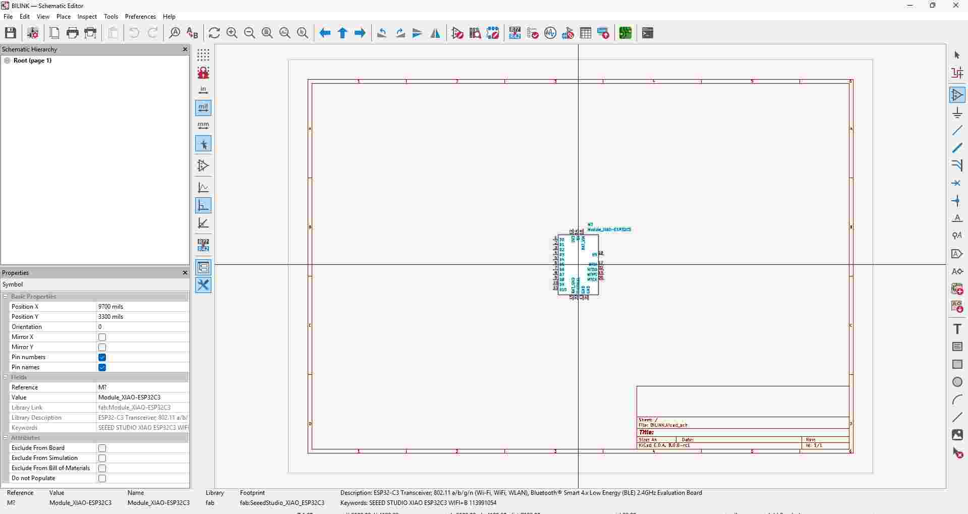
After selecting the Module_XIAO-ESP32C3 symbol, I clicked on the schematic worksheet to place it. This action positioned the component visually in the design space, allowing me to proceed with arranging additional parts and making electrical connections within the schematic layout.
This week, I came across a project video that deeply inspired me. The design, concept, and execution captured my interest, and I found it highly relevant to my learning goals. I am now motivated to replicate the project, applying my own ideas and improvements along the way.
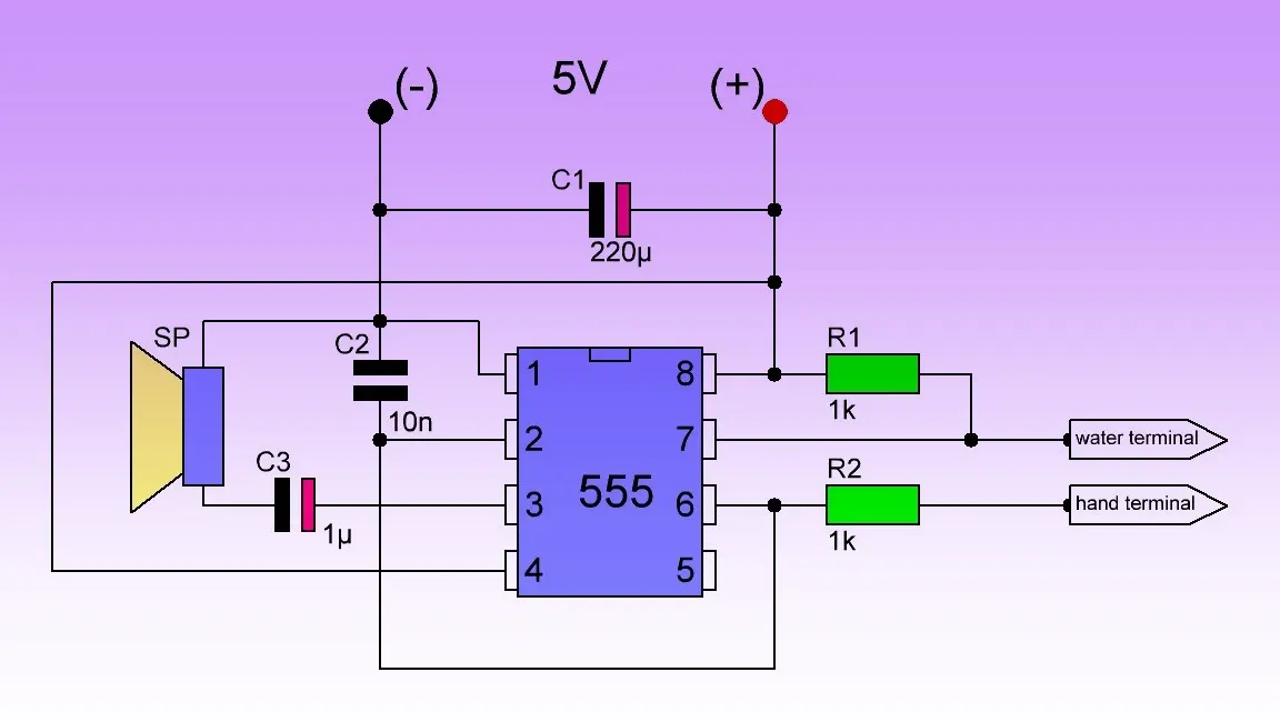
To better understand the electronic design and replicate the project accurately, I referred to a circuit diagram available online or shared within the community. This diagram served as a foundation for my schematic in KiCad, helping me identify correct connections, components, and layout strategies for implementation.
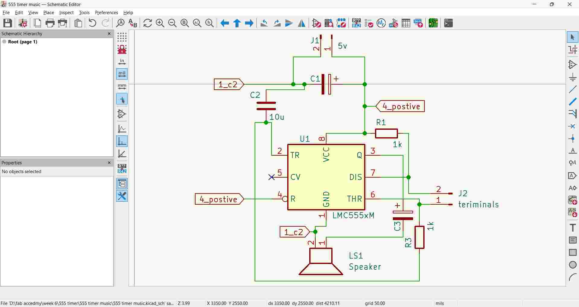
Following the reference circuit diagram, I created the schematic output in KiCad. I carefully placed and connected the components according to the diagram, ensuring that the electrical design matched the reference. This step allowed me to create an accurate schematic representation, ready for the PCB layout.
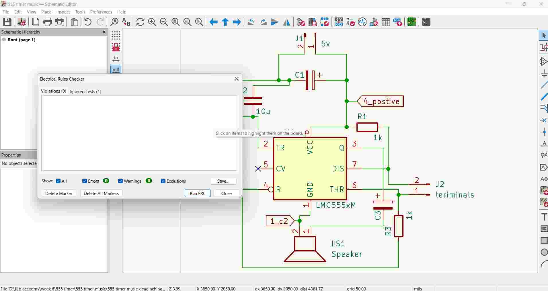
Electrical Rules After completing the schematic design, I ran the Electrical Rules Checker (ERC) in KiCad. The ERC tool helps ensure that there are no electrical errors, such as unconnected pins, shorts, or incorrect component values. This step is crucial to verify the integrity of the circuit before moving on to PCB layout.
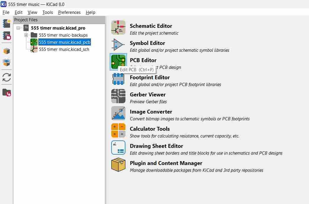
Once the schematic was verified and free of errors, I switched to the PCB Editor in KiCad. This allowed me to start designing the printed circuit board (PCB) layout by placing components and routing the connections between them, transforming the schematic into a physical board design.
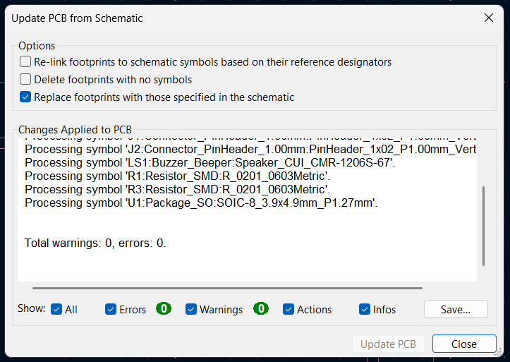
To synchronize the schematic with the PCB layout, I used the “Update PCB from Schematic” feature in KiCad. This action transferred the components and their connections from the schematic to the PCB editor. It ensured that the physical design matched the schematic and was ready for placement and routing.
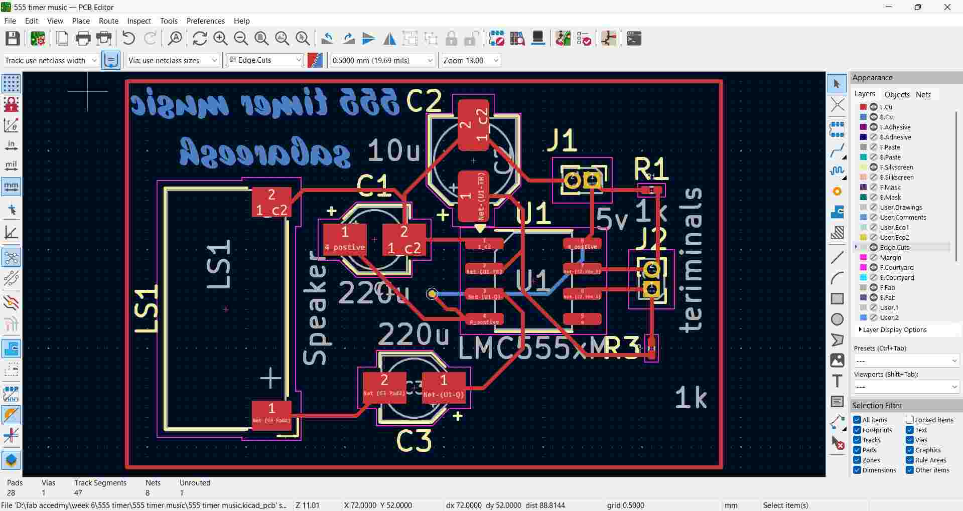
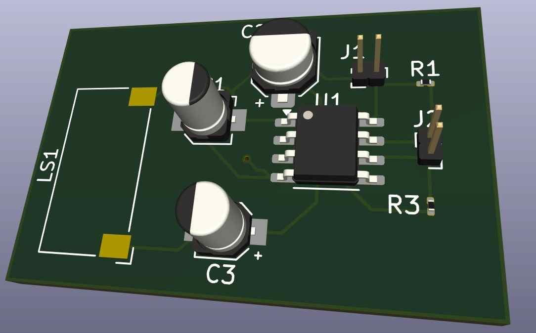
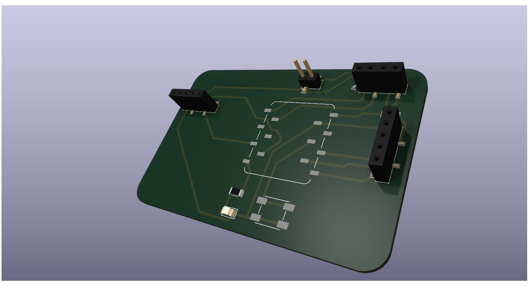
In the PCB Editor, I finalized the layout of the components by arranging them based on the updated schematic. After placing the components, I proceeded with routing the electrical connections between them. This step produced the final PCB output, which is now ready for manufacturing or further verification.
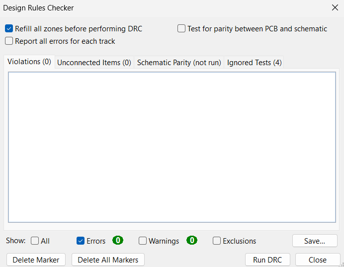
After completing the PCB layout, I ran the Design Rules Checker (DRC) in KiCad. This tool ensures that the PCB design adheres to the specified manufacturing constraints, such as track width, clearances, and component spacing. It helps identify any violations or issues before proceeding to fabrication.
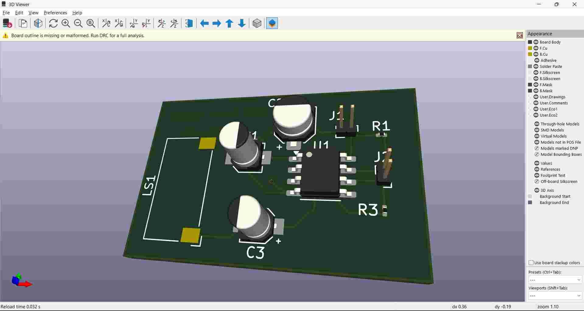
Once the PCB design was complete and validated, I used the 3D Viewer in KiCad to visualize the final design. This tool provided a realistic 3D representation of the PCB, helping me check the component placement, board thickness, and overall design for any potential issues before moving to fabrication.
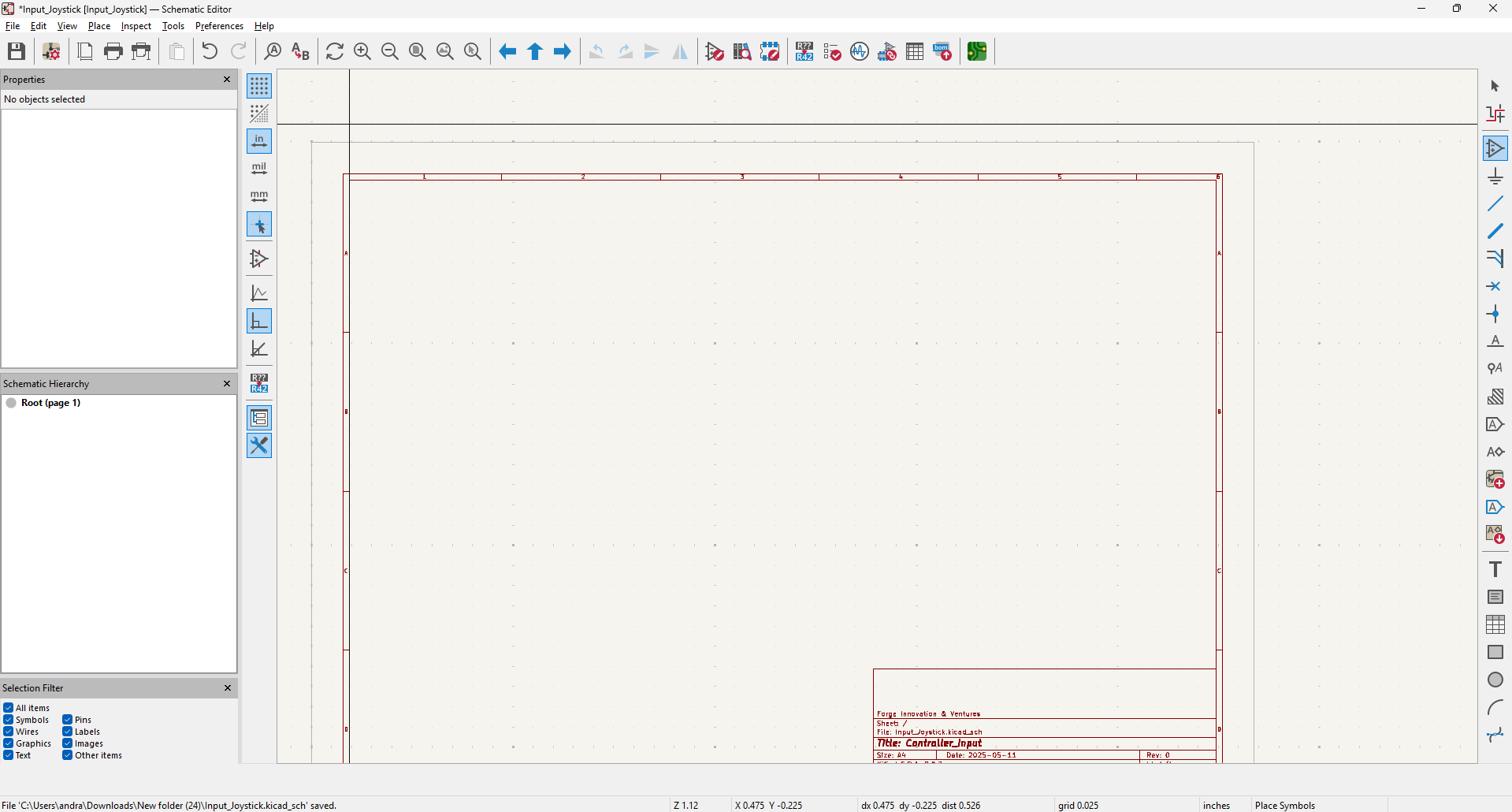
I opened the KiCad software and navigated to the schematic editor to begin designing the circuit. This is where components are placed and connected to represent the electrical design before moving on to PCB layout.
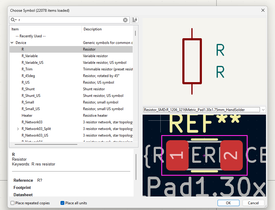
I began adding the necessary components by selecting "Place Symbol" using the shortcut key "A". This allowed me to search and choose the appropriate symbols for my circuit design.
After selecting the required components in the schematic, I proceeded to assign or verify their corresponding footprints. This ensures that each component has the correct physical layout for the PCB design and is essential for accurate placement during board layout.
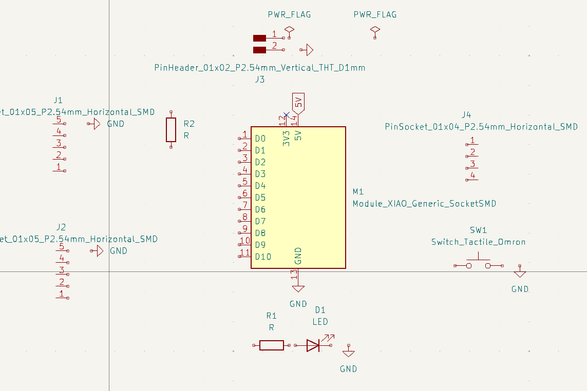
I selected specific components essential for both the schematic design and PCB layout in KiCad. Each component was chosen based on its role in achieving the desired functionality.
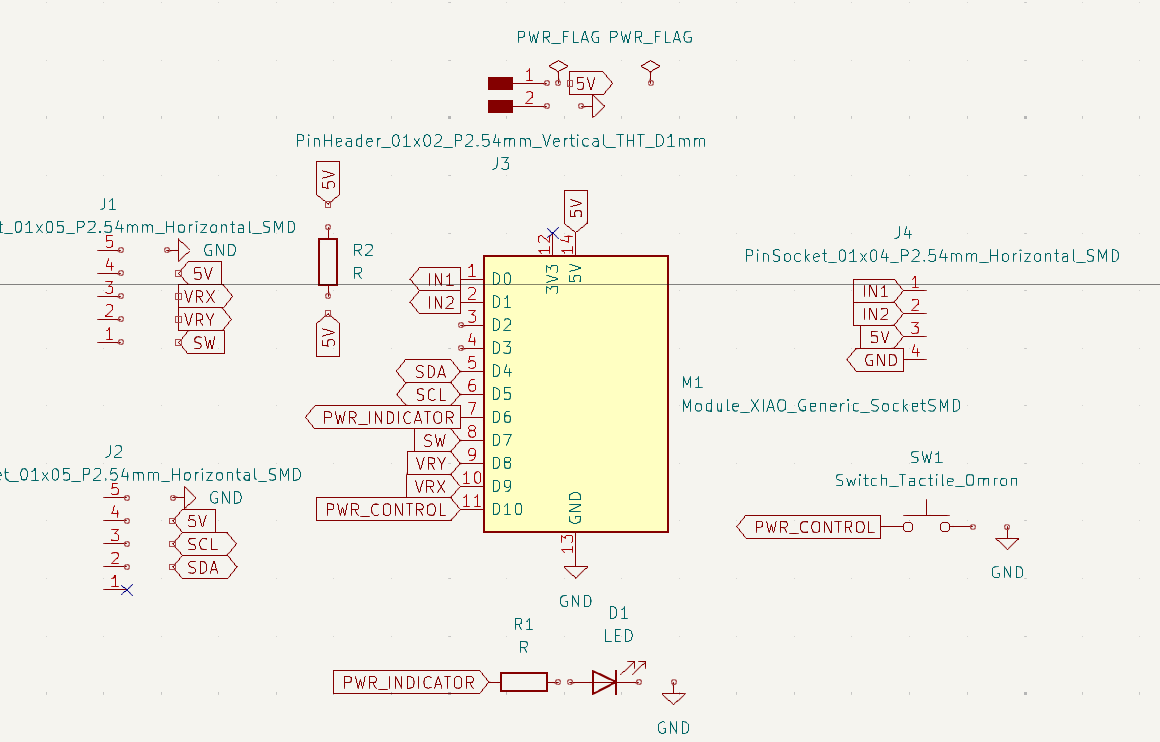
After placing all the required components in the schematic editor, I proceeded to add labels to the key signal connections. This helps in identifying and organizing the circuit, making it easier to trace signals and maintain clarity.
After placing all the required components in the schematic editor, I connected them using the wire tool. These wire connections represent the electrical paths between the components, ensuring proper signal flow and power distribution. I followed standard design practices to maintain a clean and readable circuit layout.
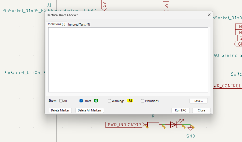
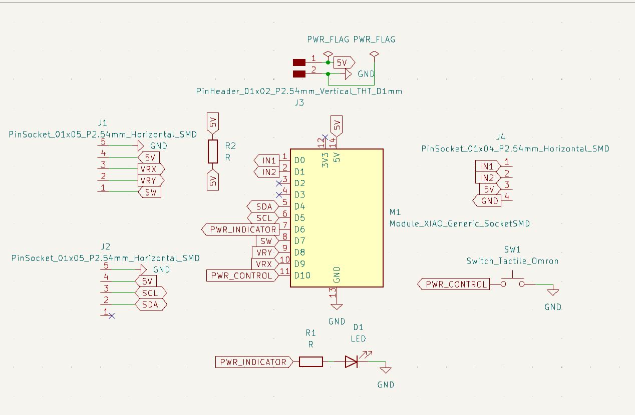
After completing the schematic and assigning all labels, I ran the Electrical Rules Check (ERC) to verify the correctness of the connections. This tool helps identify any potential issues like unconnected pins, missing power connections, or incorrect component placements. Resolving ERC errors ensures the schematic is ready for PCB layout.
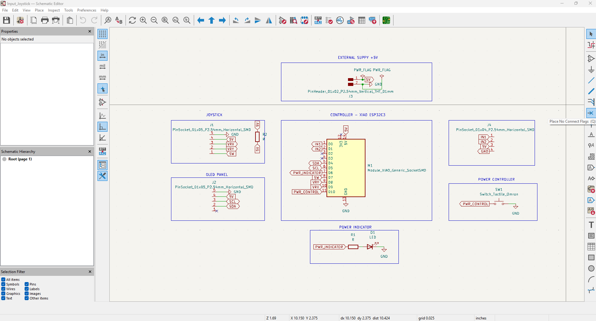
To enhance clarity and organization, I segregated the schematic into separate functional blocks based on the operations of each section—such as power supply, microcontroller interface, and sensor connections. This modular approach helps in easier understanding, debugging, and future upgrades by clearly distinguishing the roles of each component group.
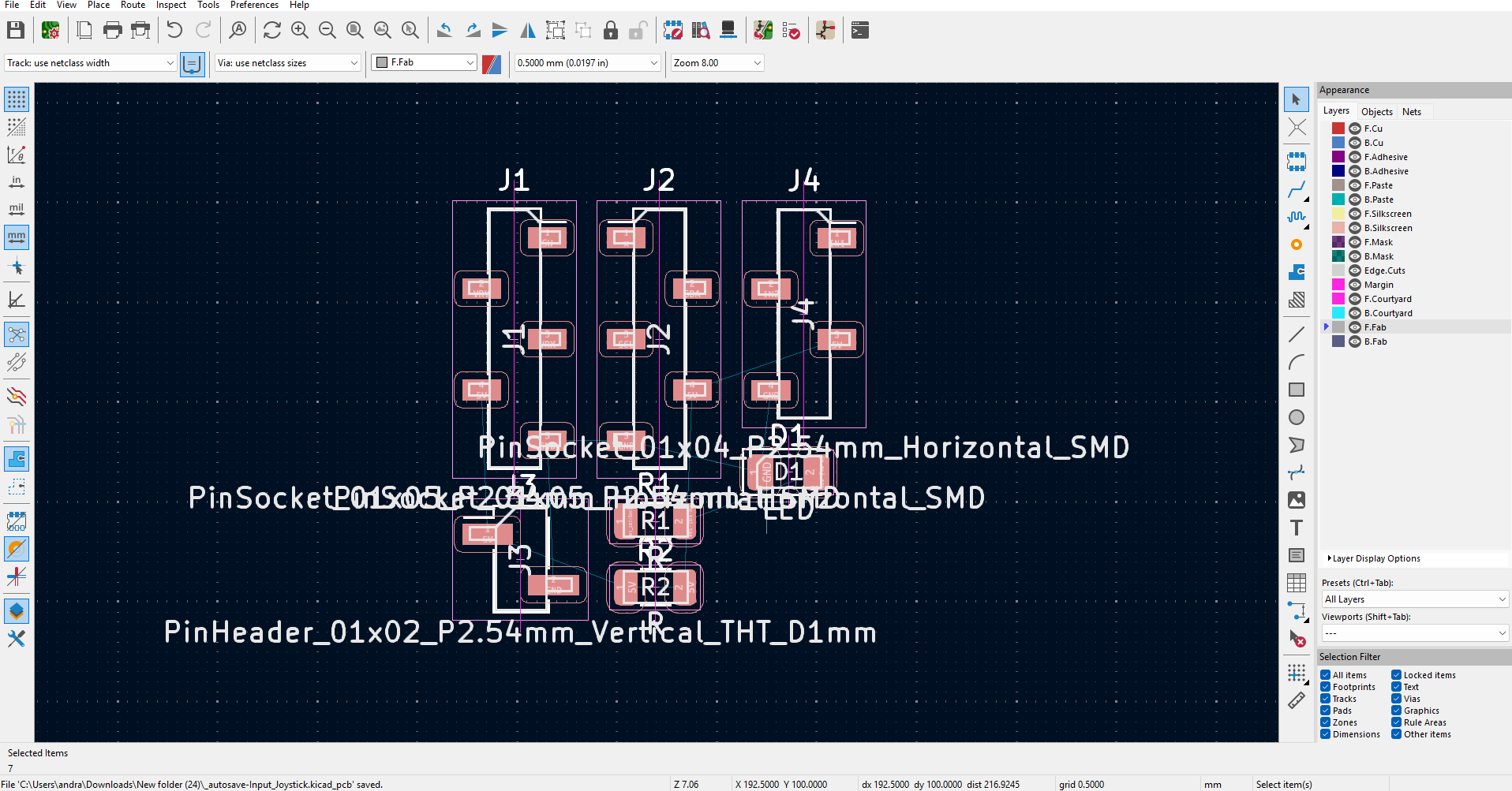
After completing the schematic and verifying connections, I switched to the PCB Editor in KiCad. Using the "Update PCB from Schematic" option, I imported all the placed components into the PCB workspace. This process ensures the schematic components are accurately transferred with their respective footprints for board layout.
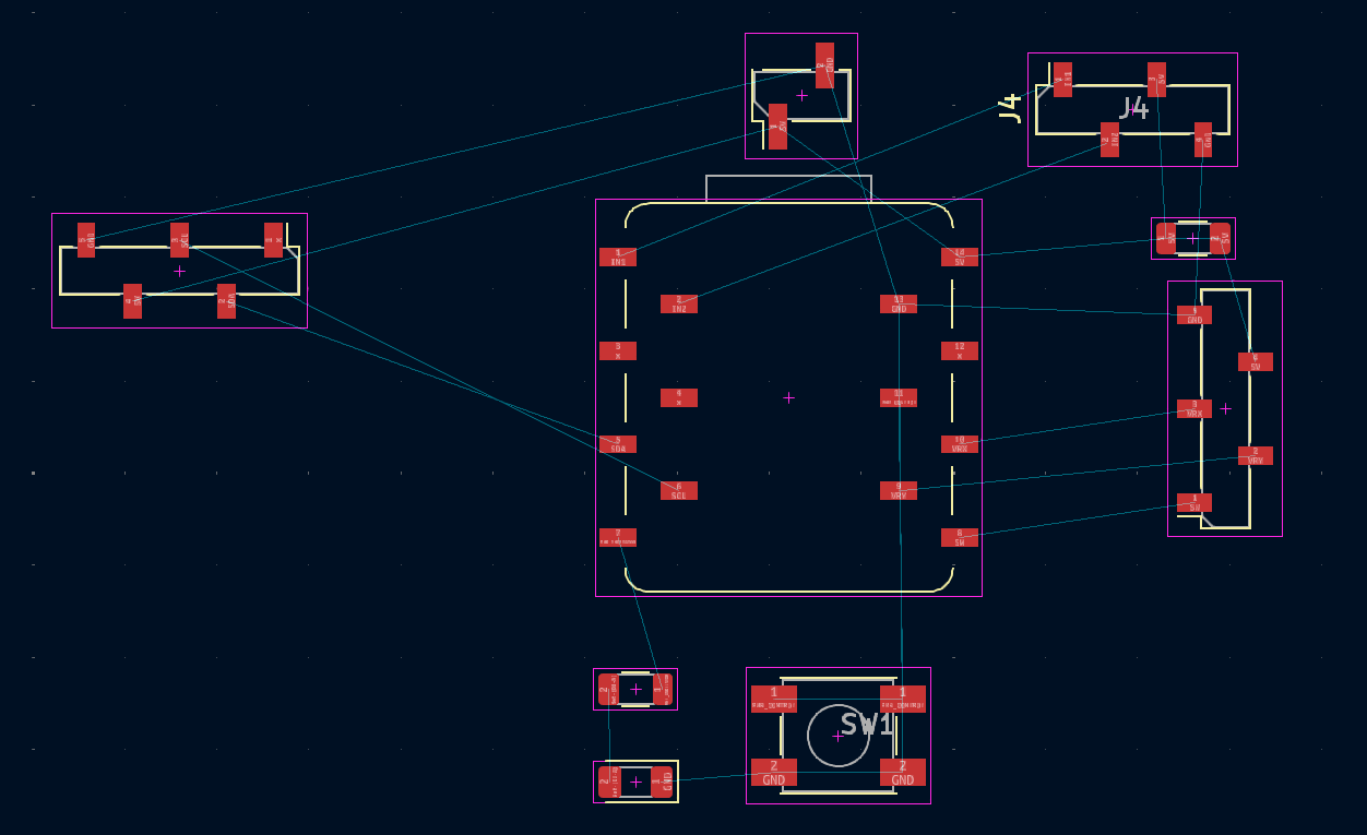
After importing the components into the PCB editor, I carefully aligned them to ensure an efficient layout and clear routing paths. To maintain a clean design view, I hid unnecessary reference texts and component descriptions. This helped in focusing on connections and optimizing space for board design and routing.
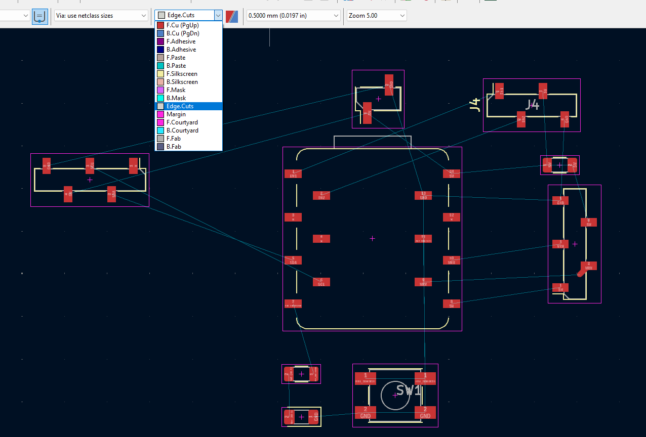
I proceeded to select the appropriate layer for the board outline and cut. By switching to the "Edge.Cuts" layer in KiCad, I defined the board’s boundary using lines or shapes. This ensures the PCB is cut precisely to the intended size during fabrication.
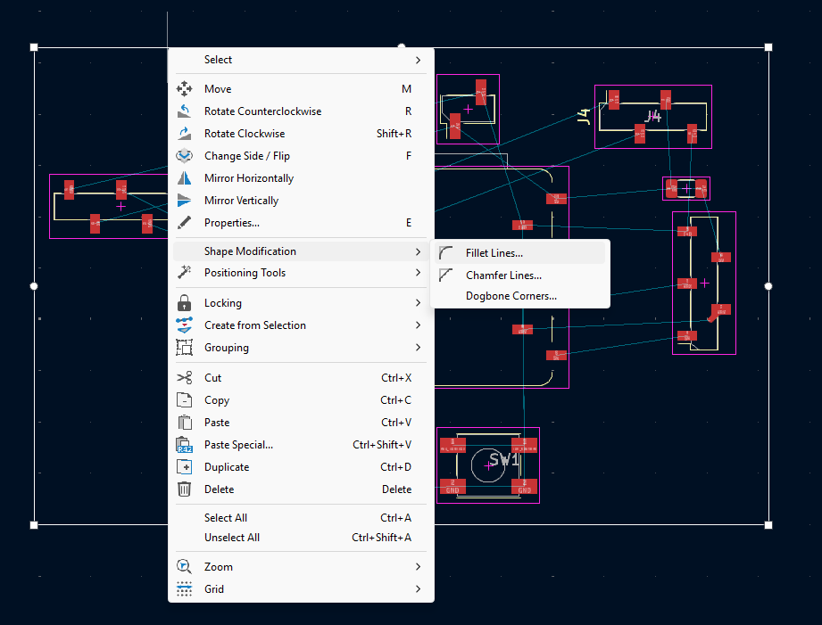
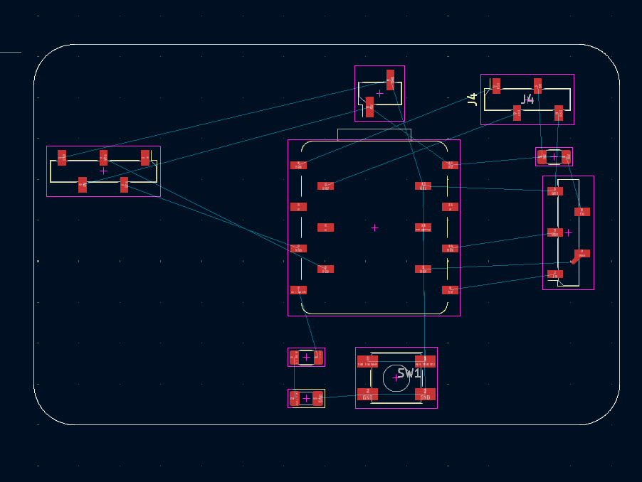
After switching to the Edge.Cuts layer, I drew a rectangle to define the PCB boundary. To smooth the sharp corners and improve both aesthetics and handling, I added fillets to each corner using the fillet tool. This ensures a clean and professional finish for the final board layout.
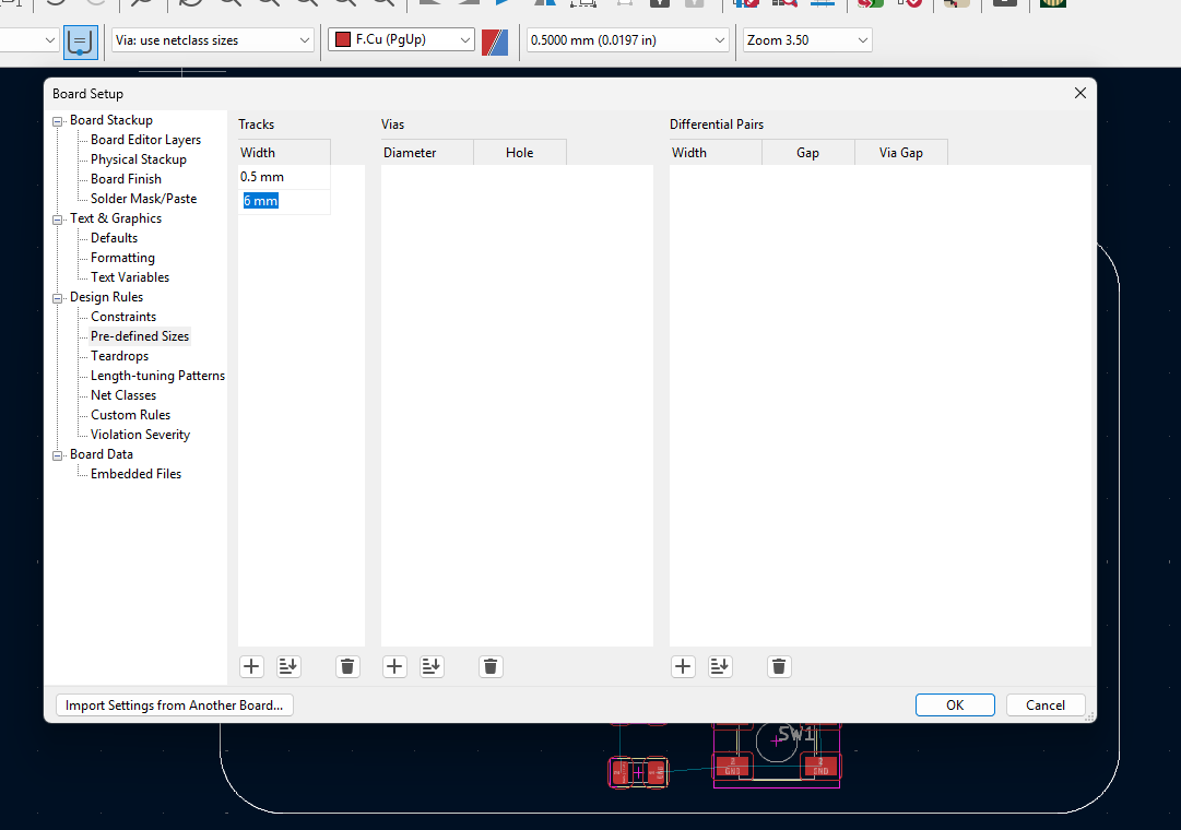
To ensure proper current flow and meet design standards, I adjusted the default track width. I navigated to the Design Rules or Net Classes settings and modified the track size from the default value to 0.6 mm. This provides better conductivity and robustness for signal and power traces.
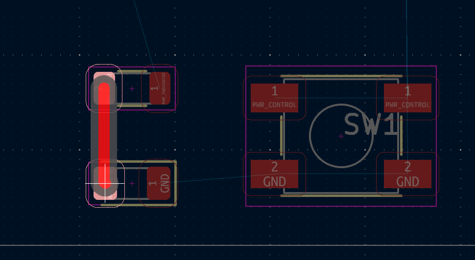
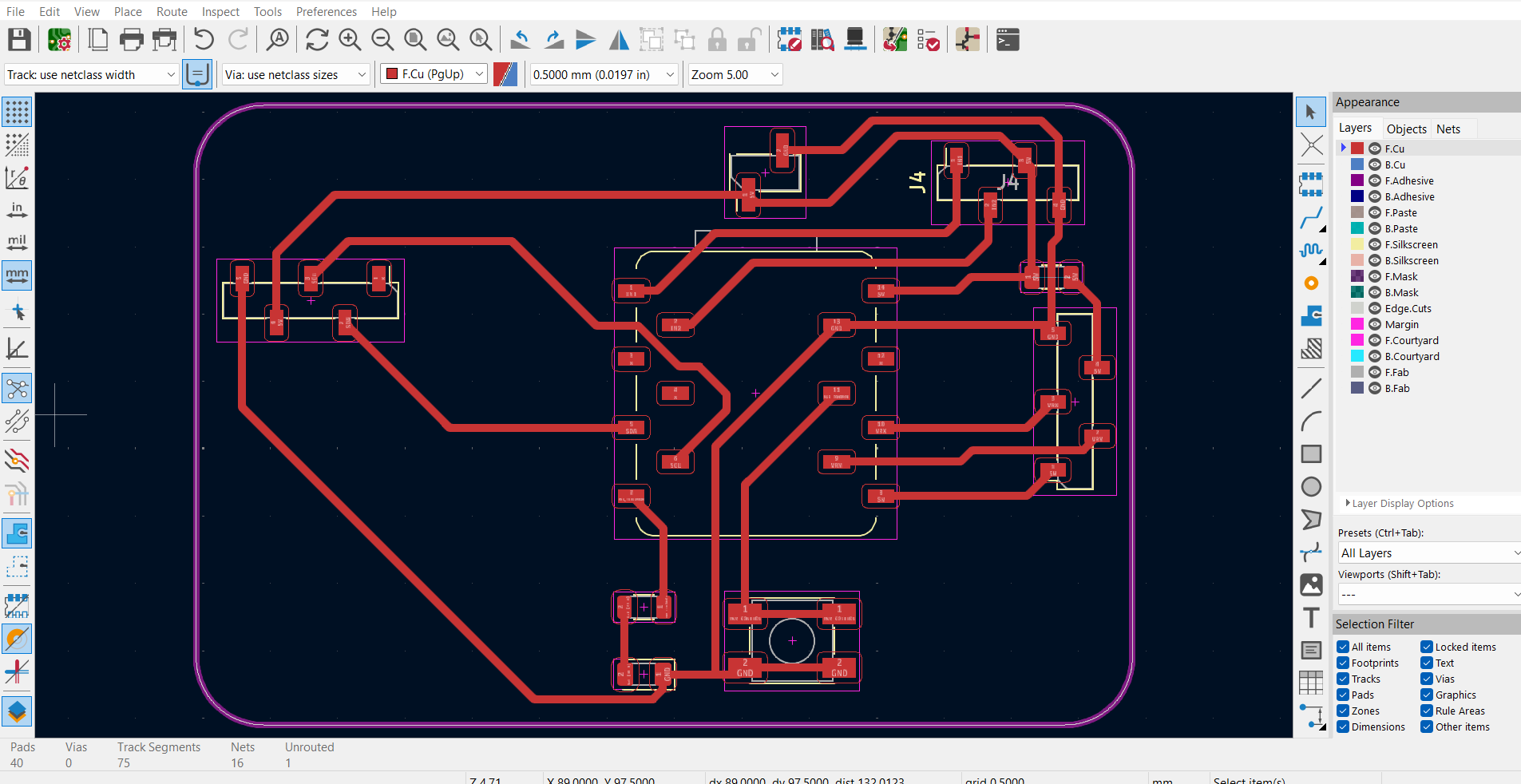
After finalizing the component placement and track width, I began routing the PCB using the Route Tracks tool. I carefully connected each component’s pins according to the schematic, ensuring optimal path routing and avoiding overlaps. This step defines how electrical signals will travel across the board, forming a complete circuit.
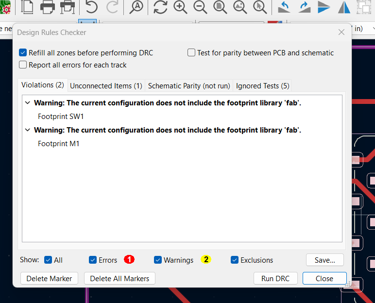
After completing the routing, I performed a Design Rule Check (DRC) to validate the PCB layout. The check reported two errors, which I carefully reviewed and resolved. This step ensured that my board met the necessary design and manufacturing standards before proceeding to the next phase of production.