Week 6 - Electronics Design
Assignment
Group assignment:
Use the test equipment in your lab to observe the operation of a microcontroller circuit board
(as a minimum, you should demonstrate the use of a multimeter and oscilloscope)
Document your work on the group work page and reflect what you learned on your individual page
Individual assignment:
Use an EDA tool to design a development board that uses parts from the inventory to interact and communicate with an embedded microcontroller
Group Page Link: The use of a multimeter and oscilloscope
Getting Started with KiCad
Downloaded and installed KiCad 9.0
Opened KiCad and created a new project: File > New Project
Two key files were generated:
Schematic Editor used to design and define the logical connections between electronic components in a circuit.
PCB Editor used to create the physical layout of the circuit on a printed circuit board, placing components and routing traces.
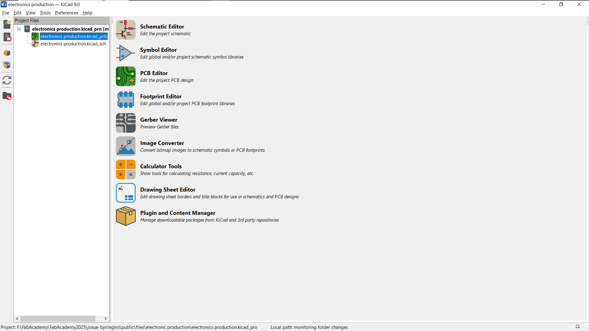
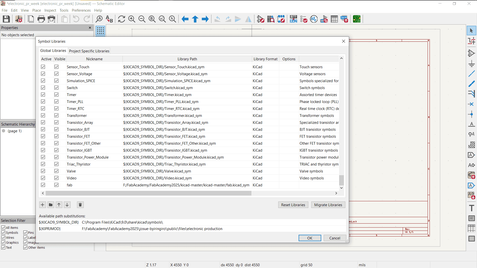
I started by adding Fab library.
Steps to add Library
Downloaded the library zip file from GitLab.Opened Preferences > Manage Symbol Libraries.
In the pop-up window, clicked Add Folder and navigated to the downloaded library folder.
Link to Fab Library
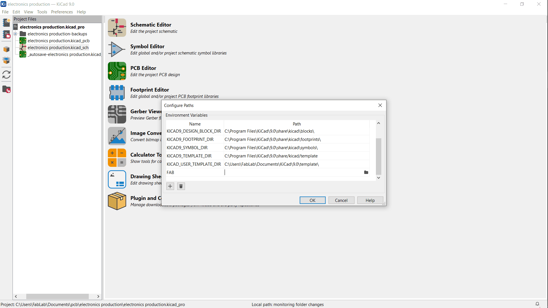
Additionally, I configured the library path for proper routing:
Preferences > Configure Path > Select Downloaded Library Folder.
Creating Schematic
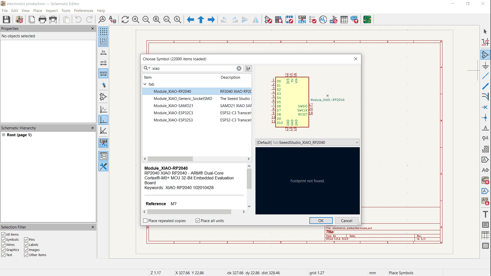
Opened Schematic Editor and added the XIAO RP2040 microcontroller using the Symbol Tool.
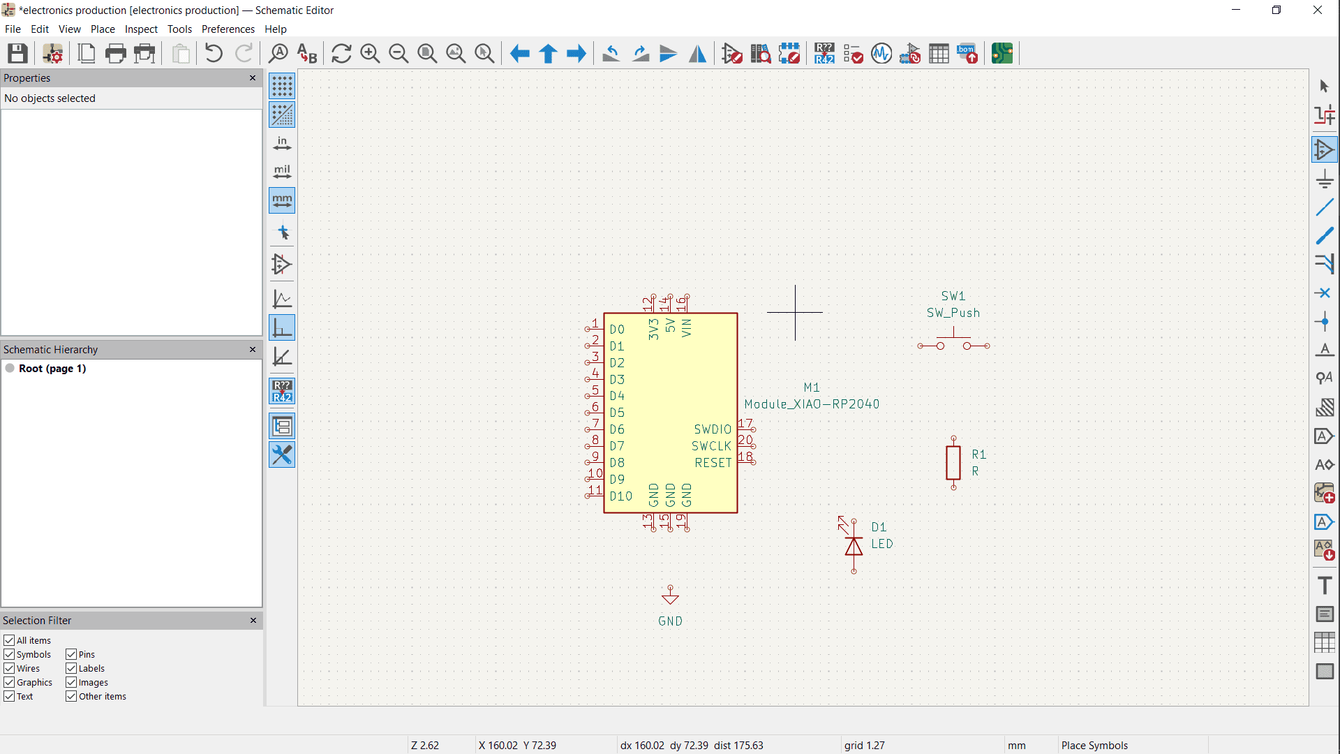
Added other components:
Two resistors
LED
Push Button
Power connections
Pins
Connecting Components
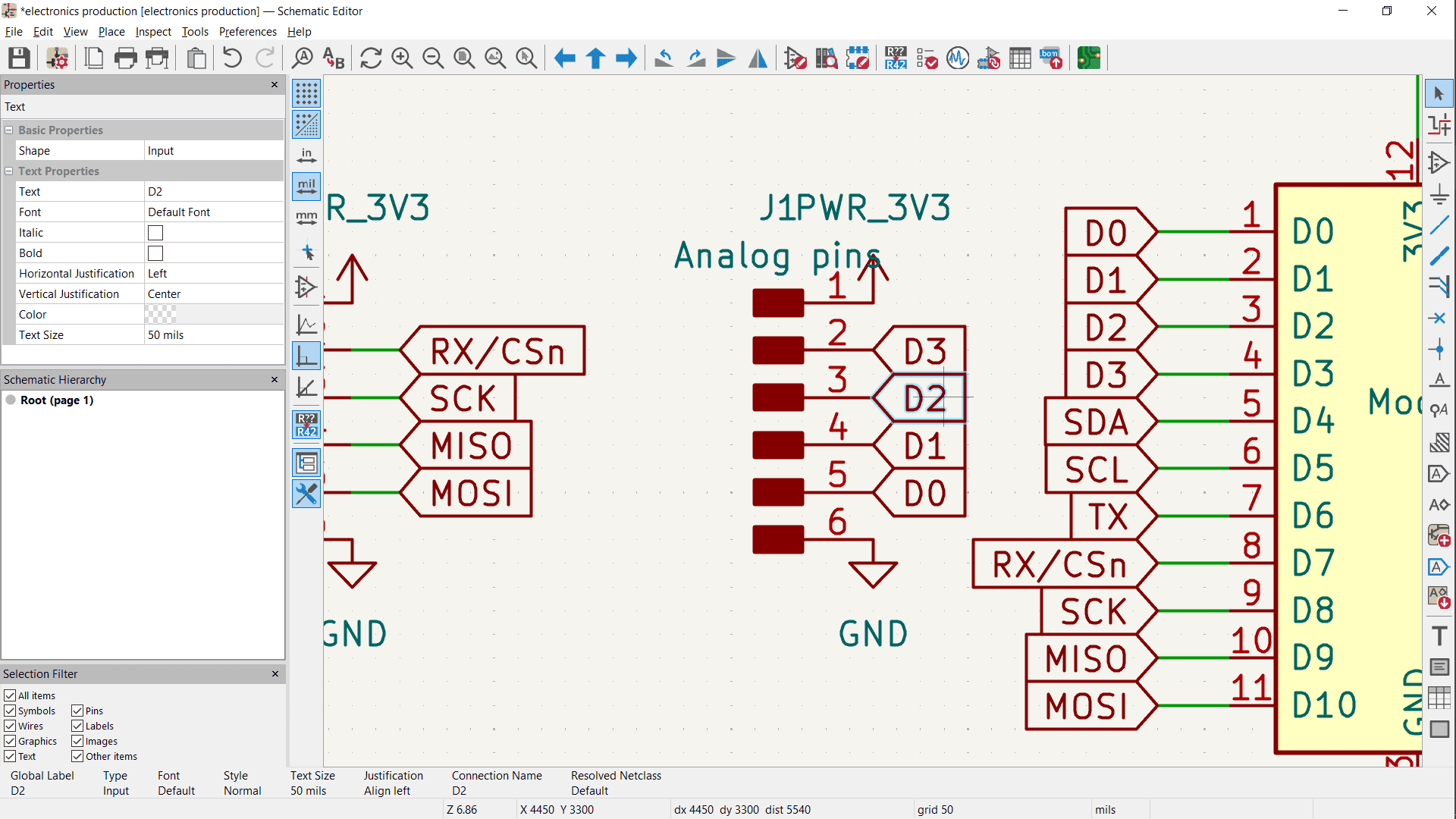
Used the Place Global Labels Tool instead of direct wiring to keep the design clean.
Named pins according to their function.
Before making connections, I extended RP2040 pins into categories: Analog, UART, SPI and I2C plus power pins to each category
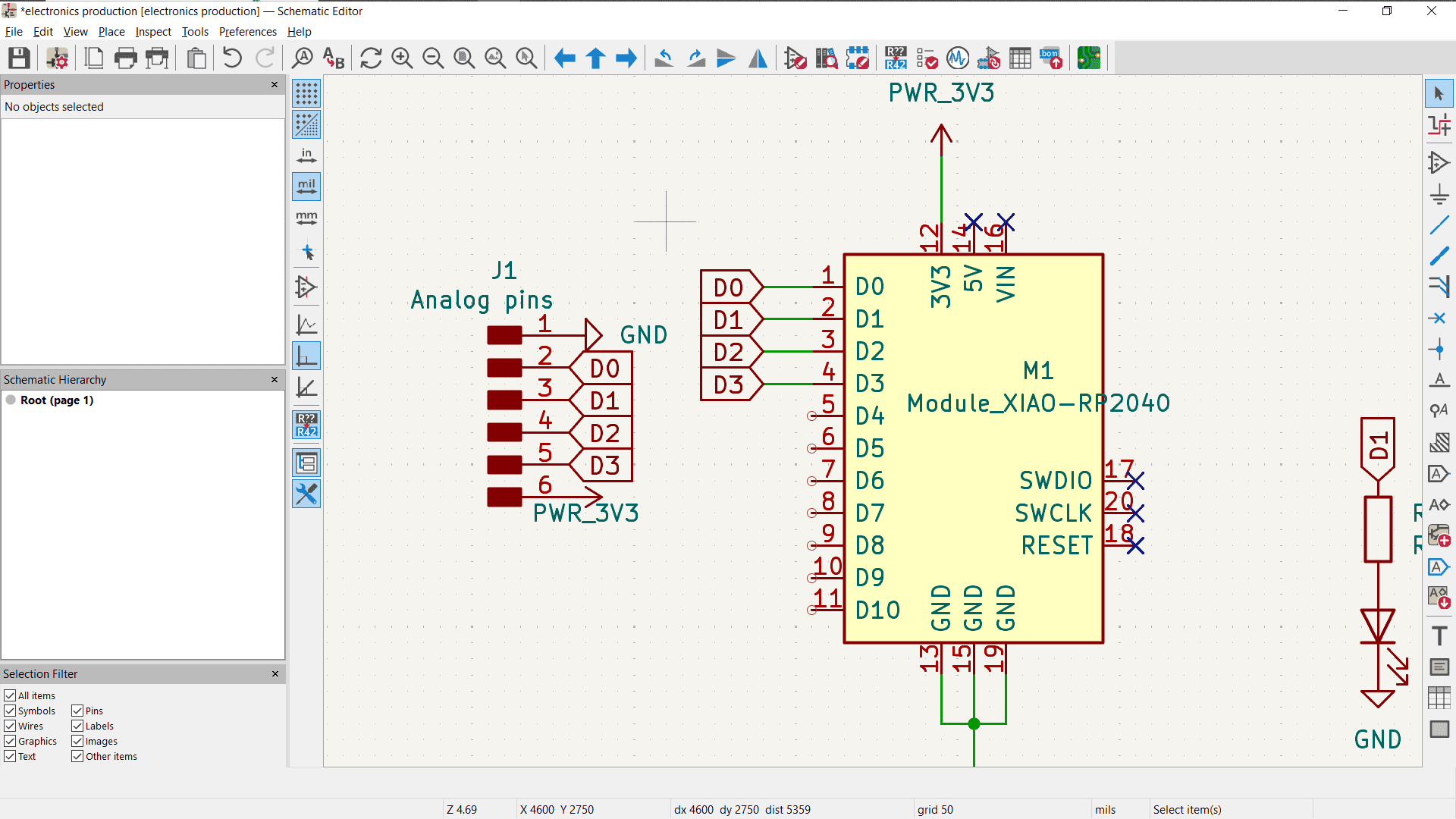
Closed unused pins using the Place No Connect Flag tool.
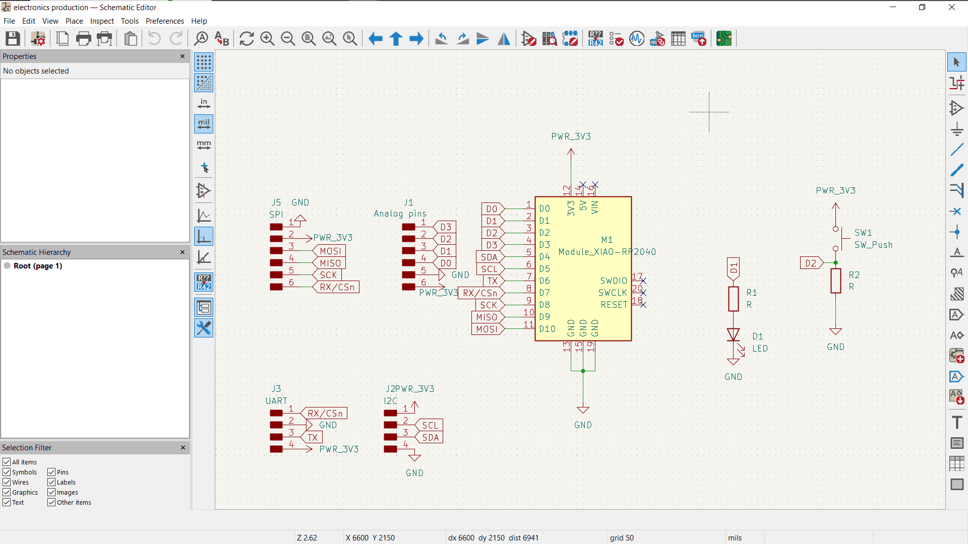
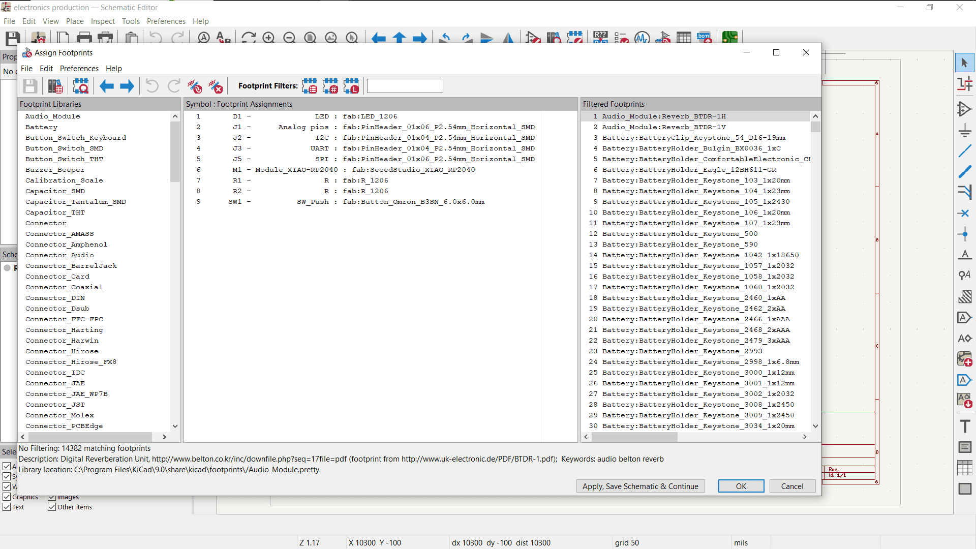
Assigning Foot Prints
Clicked on Assign Footprints.
Verified the assigned footprints in the pop-up window.
If needed, manually selected the correct footprint for each component.
Applied and saved changes: Apply & Save > OK.
Switching to PCB Editor
After foot prints I switched to PCB Editor.
In PCB Editor, I updated the PCB from schematic editor and placed it in editing area.
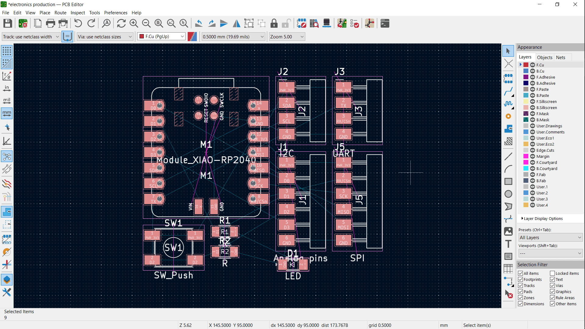
Optimized component placement for better track routing.
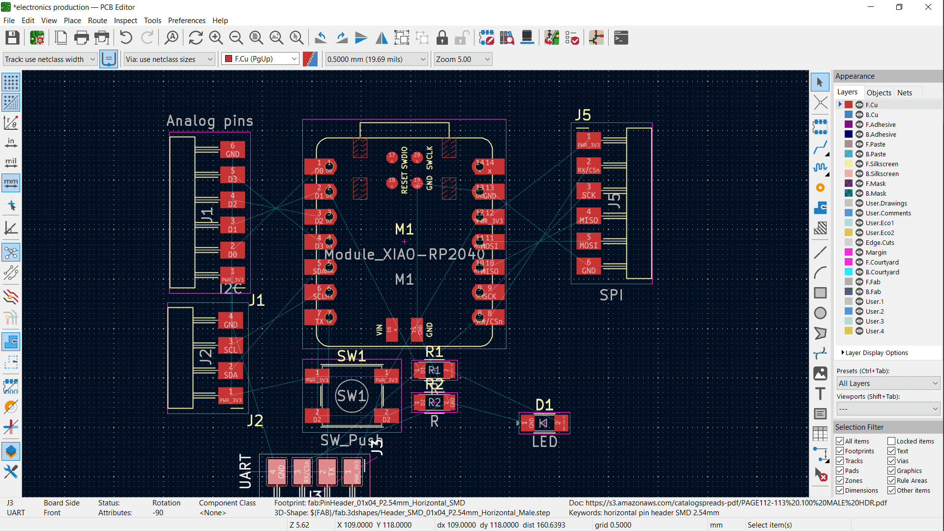
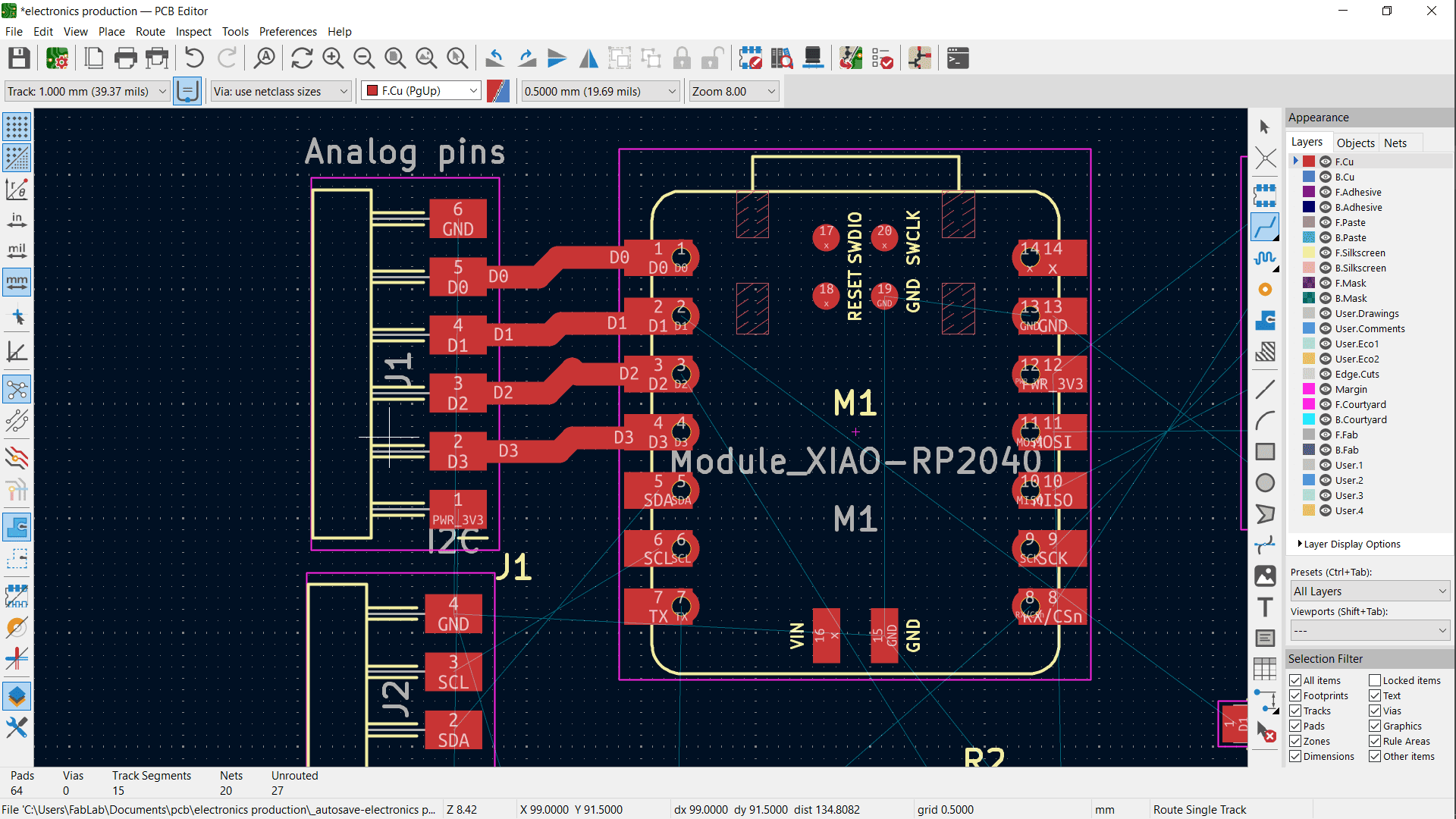
Routing PCB
Set track thickness to 1mm.
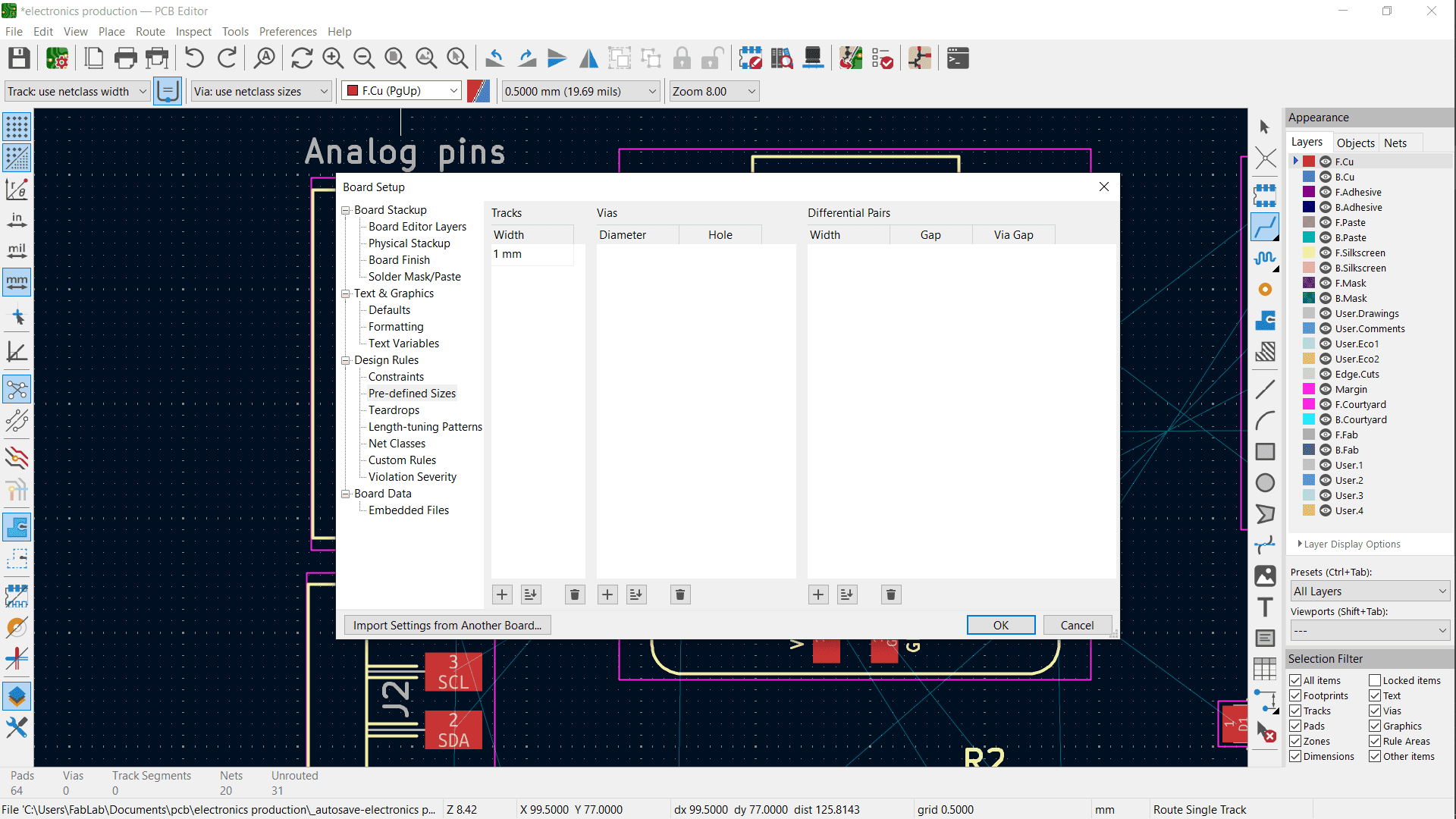
Added tracks carefully, ensuring minimal crossover.
When necessary, returned to Schematic Editor to realign pins for better routing.
Every update in the schematic required updating PCB in PCB Editor before applying changes.
After completing track routing, added edge cuts to define the PCB shape.
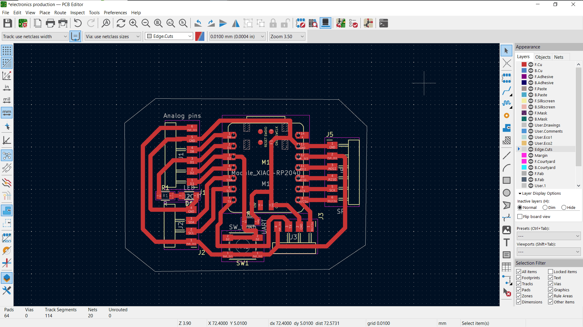
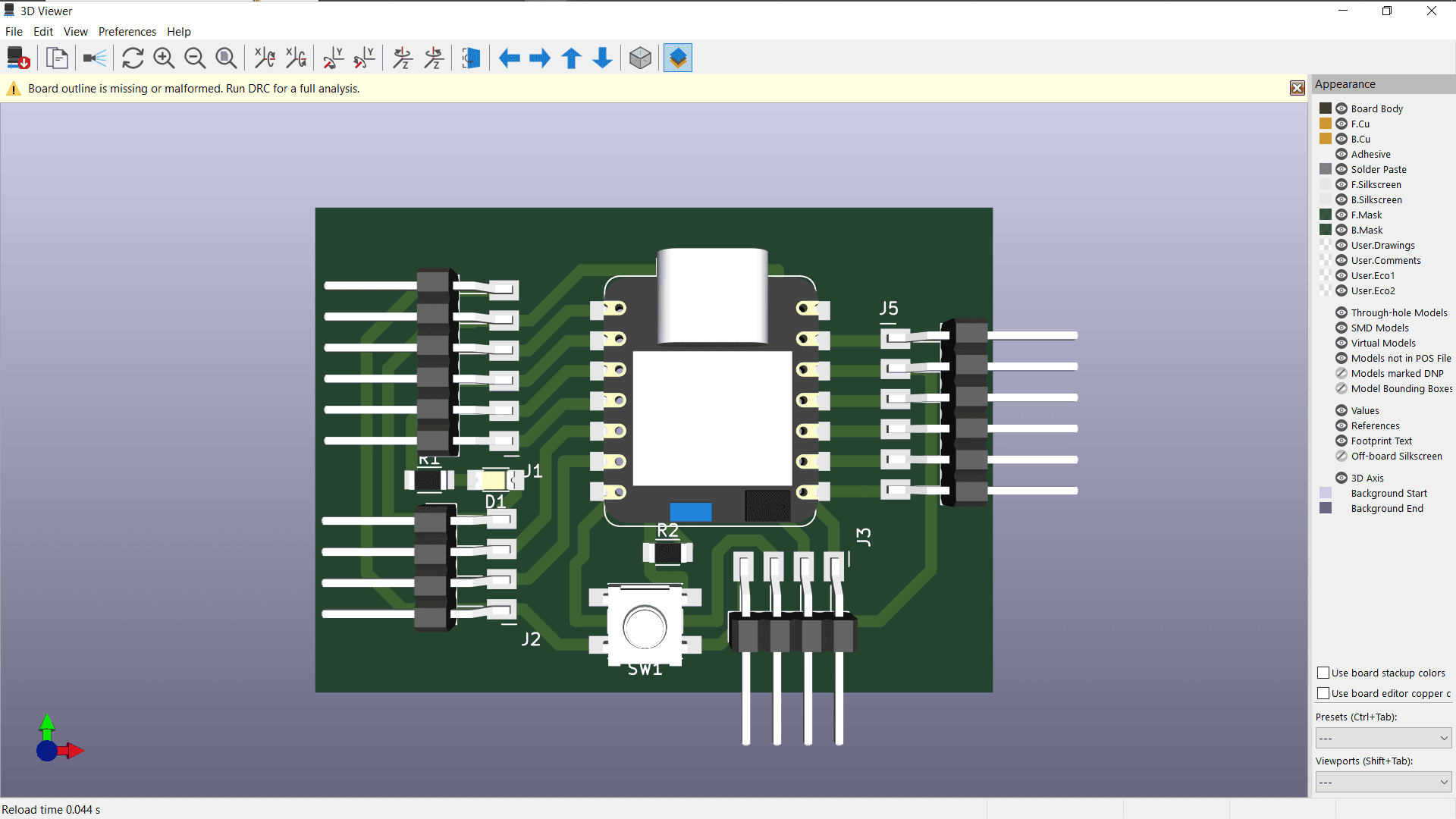
Viewed the final PCB design in 3D mode to check for any improvements.
