Electronics Design
Here's a summary about what you'll see next:
- 1) Group Assignment:
-
- Multimeter
- Oscilloscope
- Virtual Logic Analyser
- 2) Individual Assignment:
-
- Schematic and ERC
- Footprint and DRC
- 3D model and Final Layout
- 3) Original Files
1) Group Assignment:
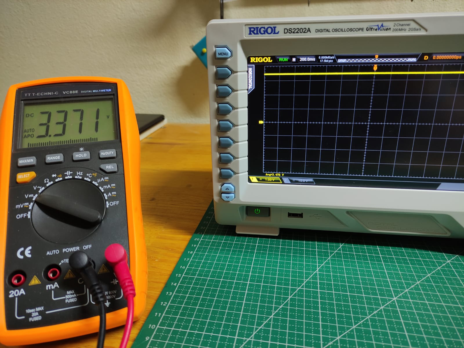
For this week we dived a little deeper in the electronics world and learned more about test equipments for circuit boards. If you have a LED that doesn't blink, a reading that doeasn't show on your LCD and don't know where is the problem? is it the sensor not reading or is it the LCD? bad wire maybe? Test Equipments are the solution.
1. Multimeter
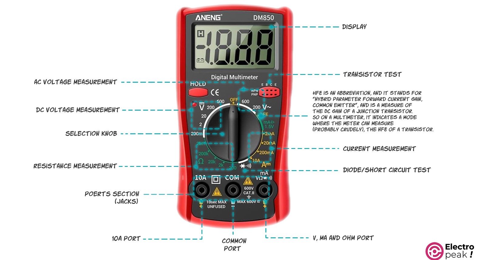
We had the UNI-T multimeter in our lab. It's a device that measures voltage, current, and resistance. It's used to measure the voltage of a battery, the current in a circuit, and the resistance of a resistor. It can also be used to check if a wire is broken. Here's a good resource to know more about it. We used the multimeter to test a simple blinking code but the delay was small so the multimeter was confused going up and down.
2. Oscilloscope
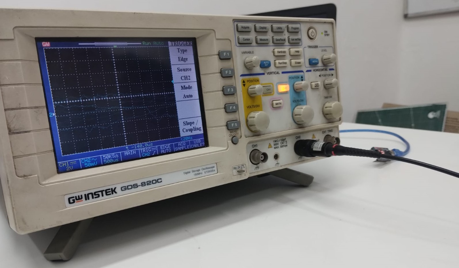
We had this old-fashioned Oscilloscope that gives 90's vibes. It is used to test and display the behavior of a signal over time. It gives you more details about how your circuit behaves. This one has 2 channels to connect probs on and the volt shows on the vertical axis and the timing on the horizontal axis. When you play with the many buttons and don't know how to get back just press the Auto set button. 😅
We tested simple circuits using it to understand how it works and what some of the buttons do and what they mean. Here in the video it was showing a fade code on a led.
3. Virtual Logic Analyser
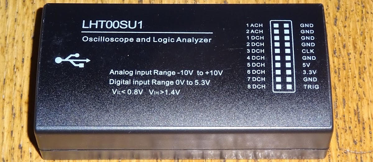
For another test equipment we had the LHT00SU1 Digital Oscilloscope and Logic Analyzer. This one should be connected to your PC or Laptop and it shows a looooot of readings on a software. We used PulseView software.
To explore it, we wrote a simple code that should send a Hello World message. The program showed the message in details. 😵
2) Individual Assignment:

One of the main reasons I wanted to join the Fab Academy was that I wanted to know more about PCB, how it works, and how to design one myself. So, this is my week. 😎 For the individual assignment we needed to use an EDA tool to design a development board that communicates with an embedded microcontroller.
I wanted to continue working in baby steps on my final project so I decided to start designing the first version of my PCB for it and use the wiring diagram I did in embedded programming week. To prepare for doing the assignment I installed KiCad and followed this KiCad Tutorial.
I also downloaded the Fab Libary and imported them to KiCad by following the installation steps.
1. Schematic and ERC
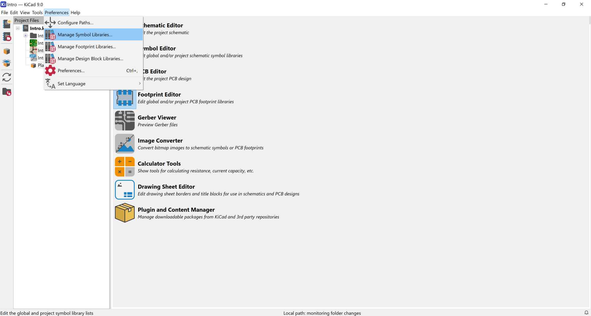
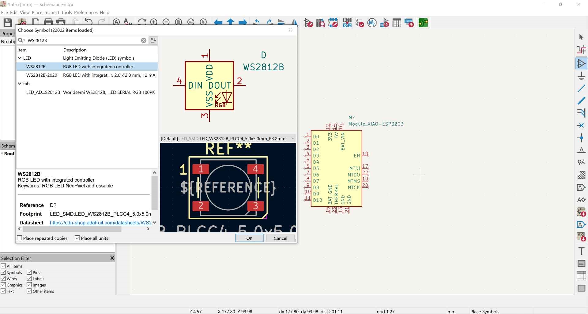
To make a PCB you go through some steps to get to the final output. First, select you components and make sure you have their symbols and footprints and the footprint matches the real component you have. To get these you can search SnapEDA. To add the components to KiCad you click on preferences -> Manage Symbol Libraries -> Add and select the library you downloaded. And also from preferences -> Manage Footprint Libraries -> Add and select the library you downloaded. And you're all set.
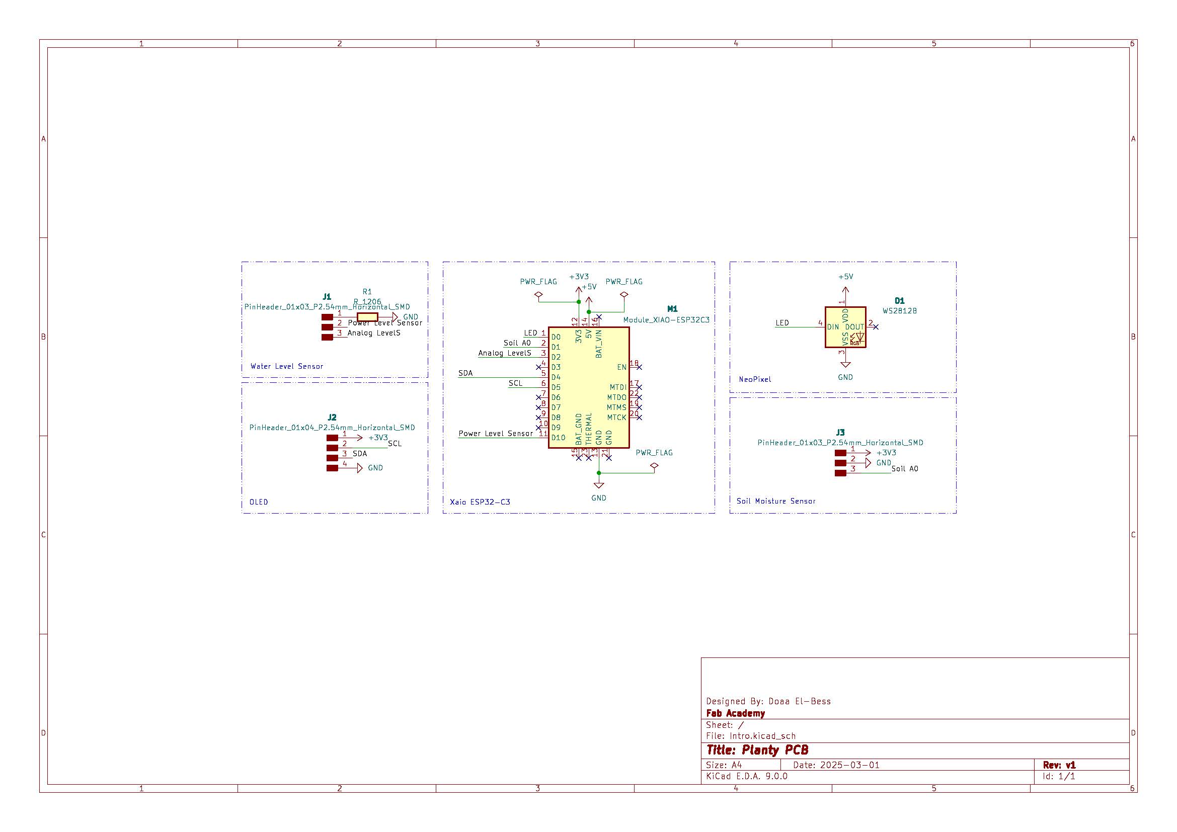
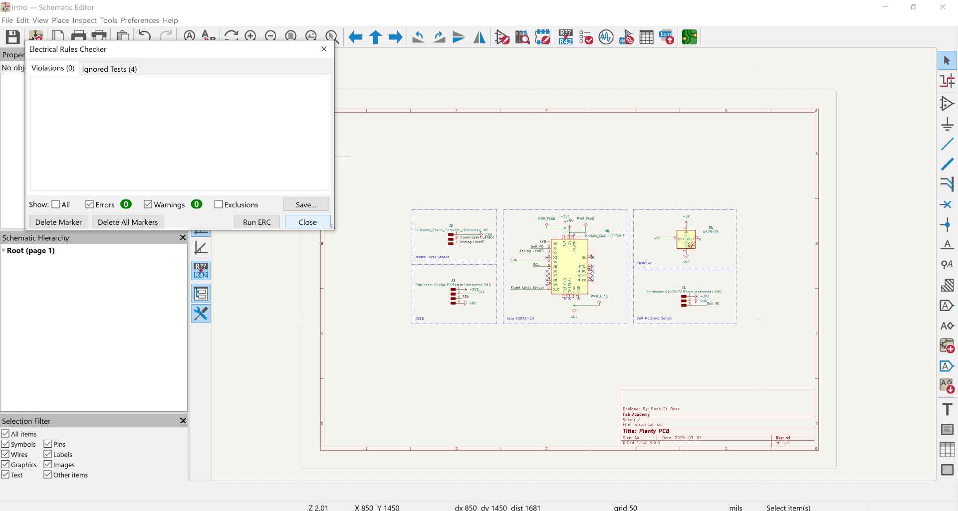
Next, you start with the schematic and connect the wires. I recommend you watch the tutorial I shared above to know how to do it step by step. But here's a brief about how I did it.
2. Footprint and DRC
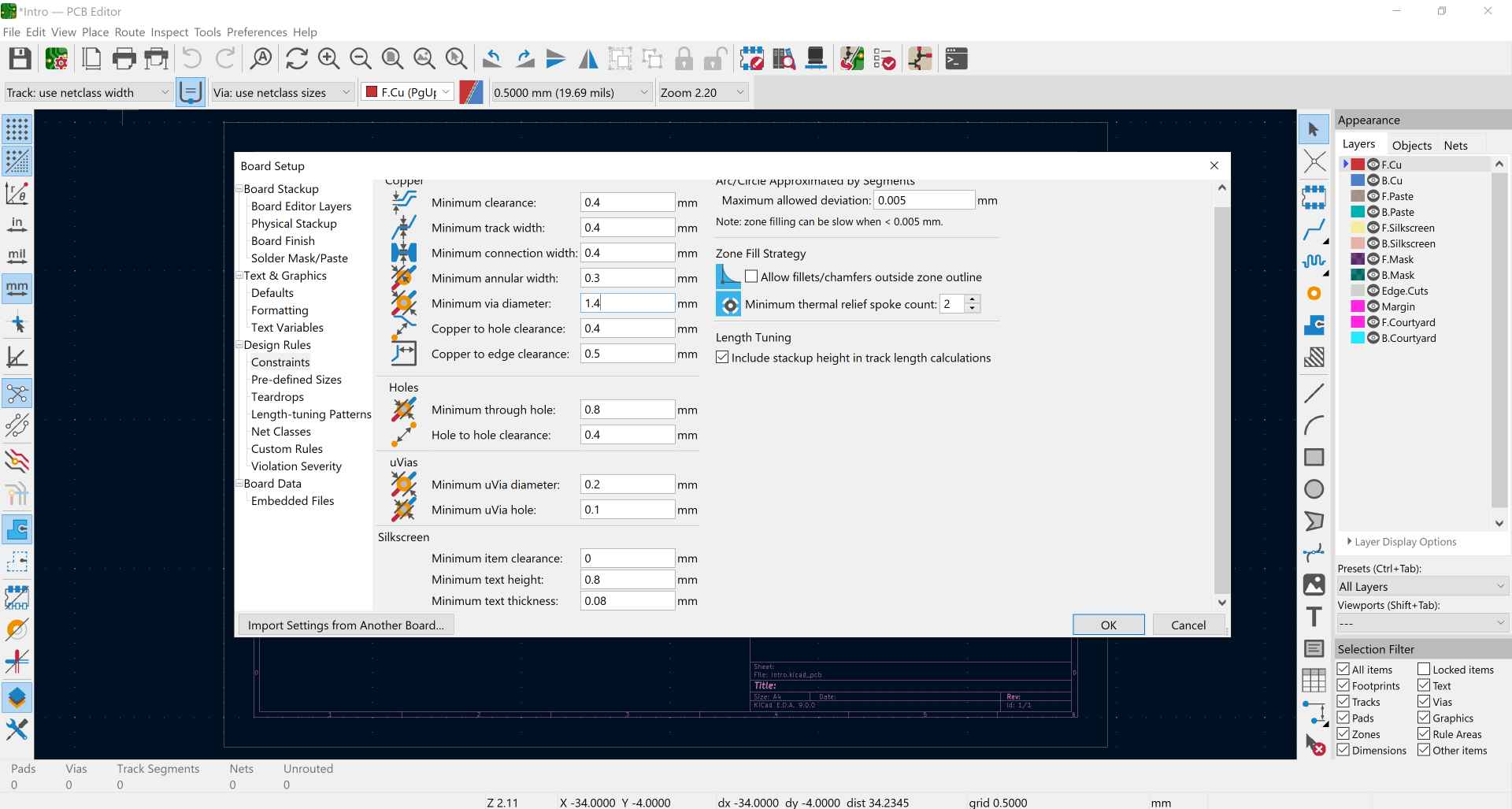
In this step I switched to the PCB Editor and before you start routing you need to go to board setup. This is where you tell the program what layers your PCB will have and set your design rules which will vary based on the machine you're using for fabrication. So, I asked my instructors in the lab and they provided me with the design rules constraints. And the other data I followed the tutorial.
I also assigned net classes for the power and signal wiring and returned to the schematic after that to assign net class for each wire by right click on it then assign net class.
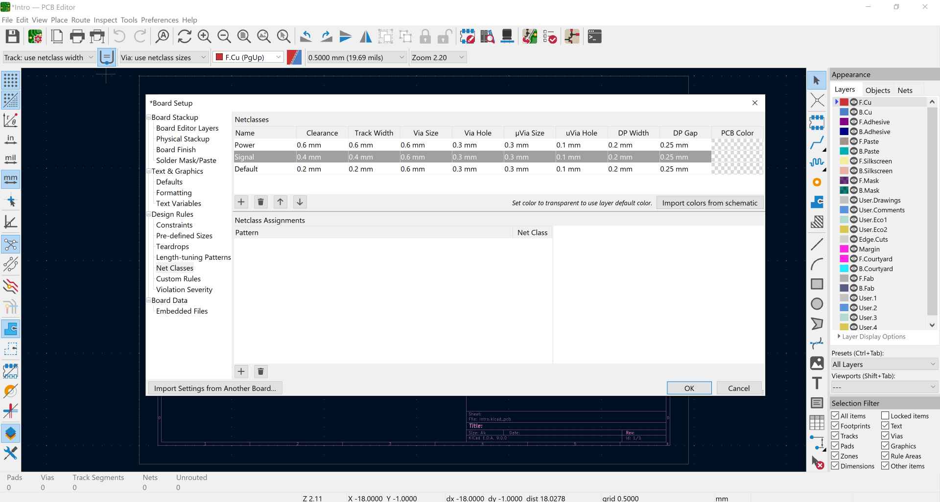
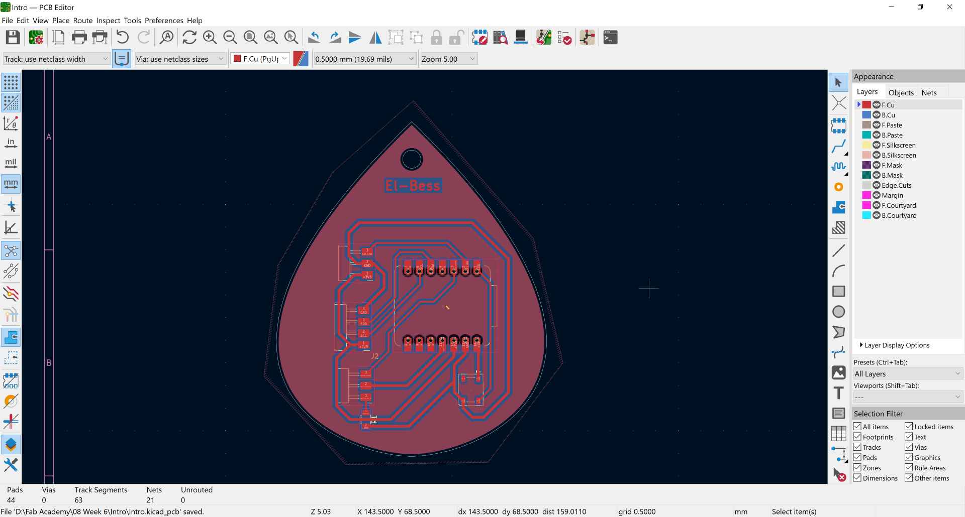
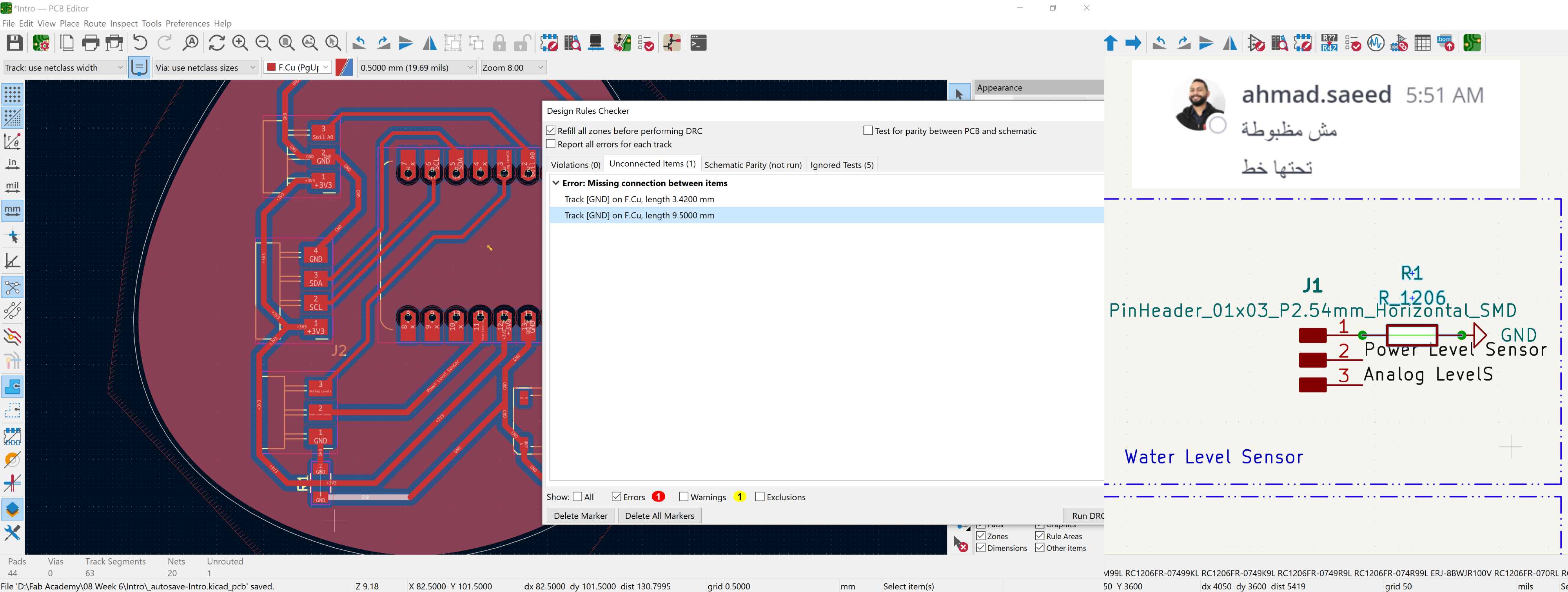
Then I clicked on the Update PCB from Schematic button to import the components to the PCB Editor. I placed the components in the board and started routing the wires. I press X then make my routing. I spent a lot of time trying to make my routing without having to put a 0 ohm resistor but I ended up returning to the schematic and adding the resistor to the only left wire without a way. When I ran a DRC it gave me errors that there are missing connections. I asked my instructor if it's okay or not so he asked me about adding it to the schematic and when I showed it to him he told me that there are another connection under the resistor.
To make the outline of the PCB I selected the edge cuts layer and used the bezier curve to make a shape like a drop of water then locked it and placed my components on it. I also added a circle to make a cut in the shape to hold the PCB from it.
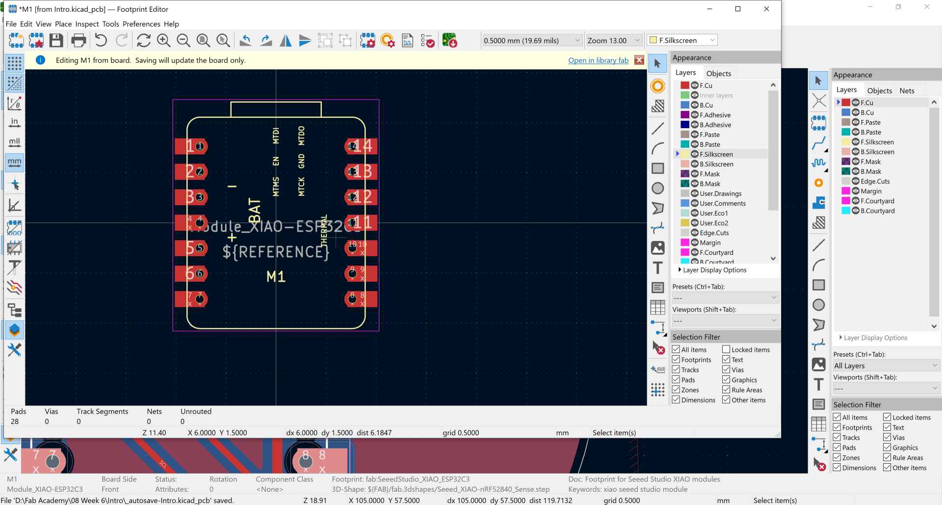
I had a problem with the xiao footprint while routing because it had some areas on the back of it and it stood in the way of my routing 😠. So I decided to get rid of them by right clicking on the xiao then selecting open in footprint editor, and removing all that I don't need as I'll be mounting the Xiao on pin headers after all.
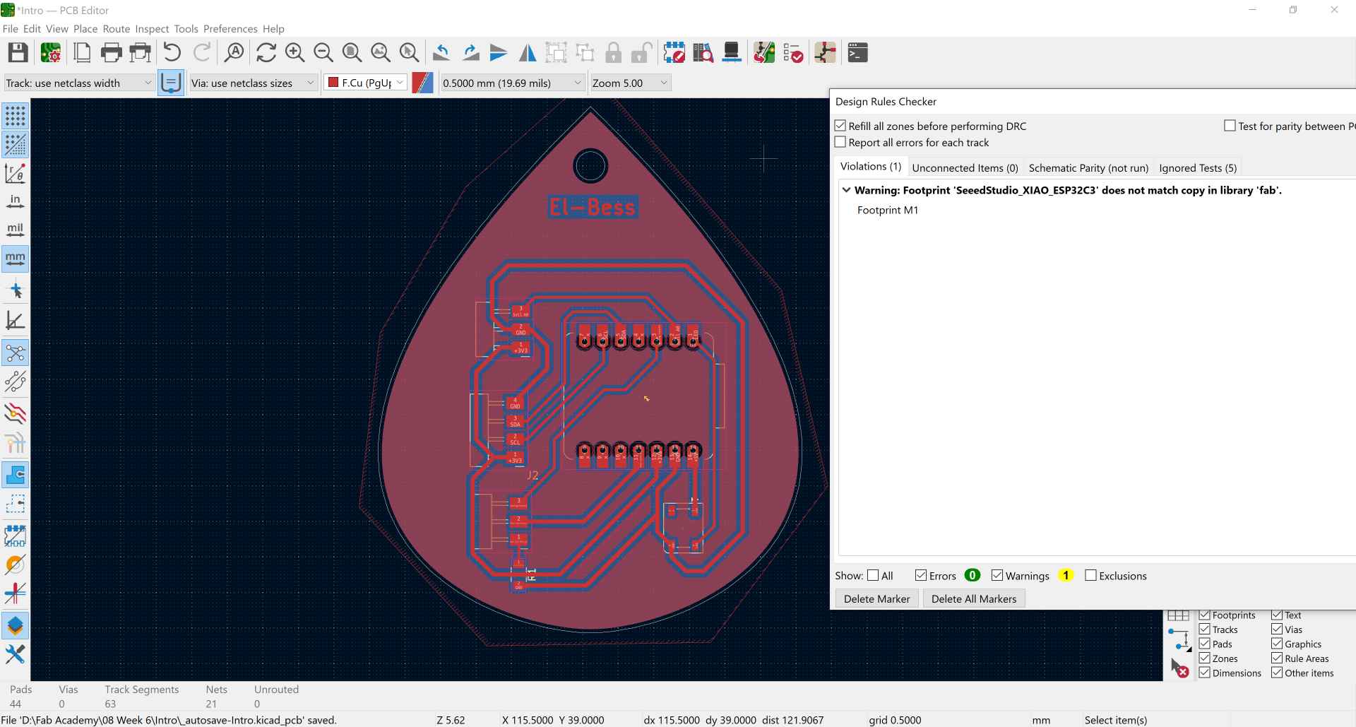
I wanted to add a personalized touch to the board so I used the Text tool to add my family name to the PCB. Finally, it's time for DRC "Design Rules Check" and it only gave me a warning of my changed footprint.
This was my first version of the PCB. As you can see the routing with the light green and all the dark green will be removed. To prevent this I used the draw filled zones tool and drew a boundary around my PCB. This makes like a stroke around each route to seperate them from each other and that stroke is the one that will be removed.
3. 3D model and Final Layout

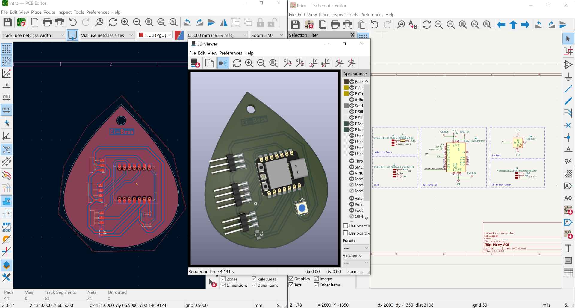
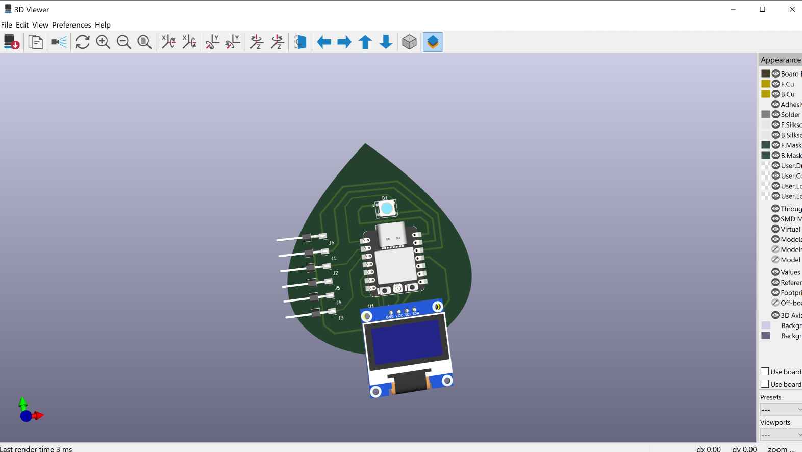
After making sure everything is good and passed ERC, DRC, and SaeedRC, I opened the 3D viewer window to render an image for my final look of the Planty PCB. I believe there will be improvements on this version in the following weeks but it was a great start for me.
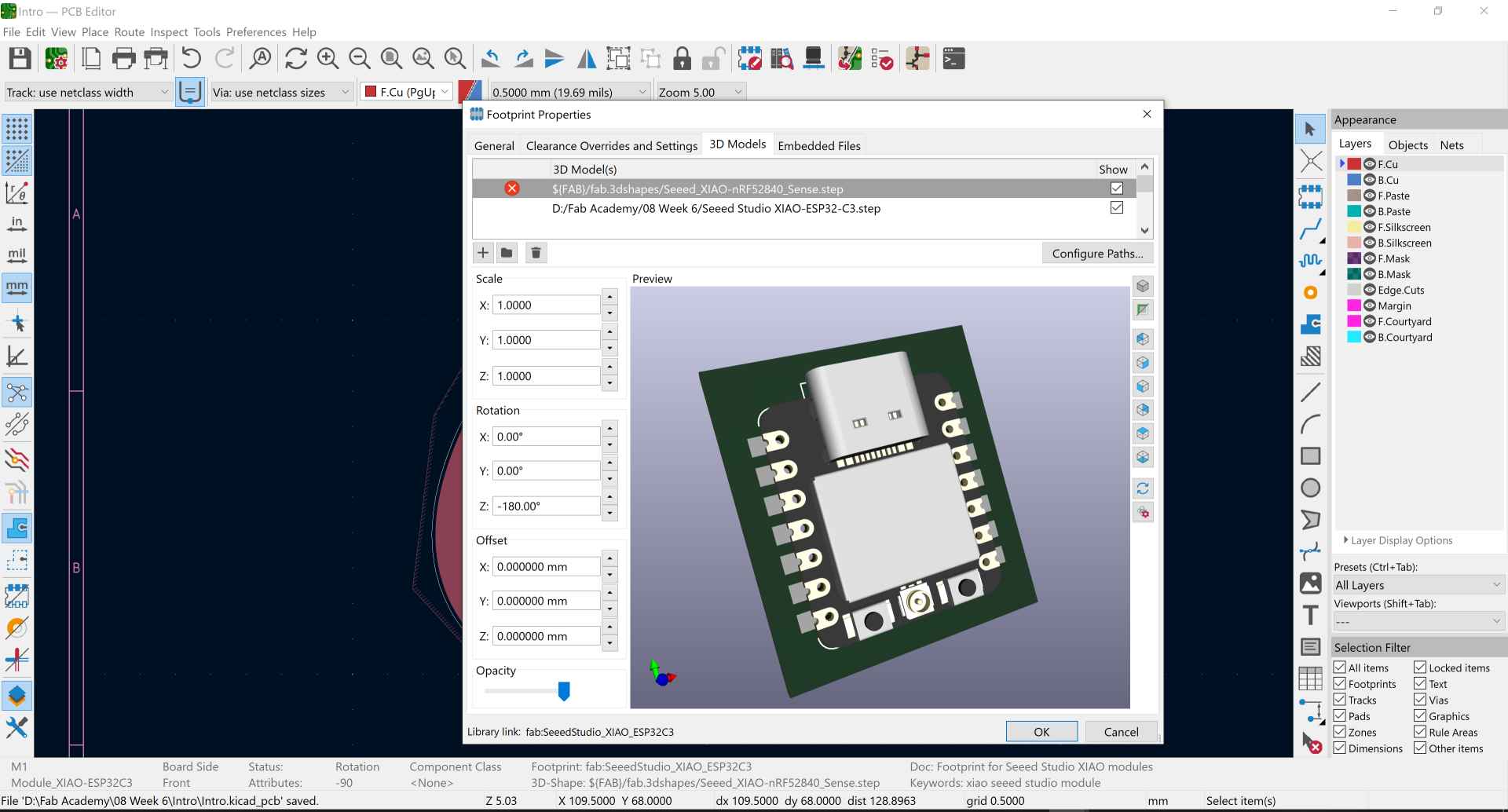
If there were any missing 3D model you can search for it on GrabCAD or any other website then right click on the components --> Properties --> 3D Model, and import the step file and position it correctly.
