Week 06. Electronics Design
From blinking LEDs to borderline wizardry - here goes one week of electronics design! 🚀✨
Assignments
Group Assignment(link):
use the test equipment in your lab to observe the operation
of a microcontroller circuit board
link to group assignment.
We learned how to use teh various tools in the lab to be able to check our boards.
individual assignment:
use an EDA tool to design a development boardthat uses parts from the inventory to interact
and communicate with an embedded microcontroller
extra credit: try another design workflow
extra credit: simulate your design
extra credit: design a case around your design
Electronics Design
I decided to use Eagle in Autodesk Fusion as ny EDA tool of choice as I already have it installed on my computer.
this weeks reading list
Getting started with electronics by Forrest M. Mims, III.
Eagle Tutorial I found this tutorial on Bo Heather Bowmans site in the electronis design week section.
I decided to keep working in Autodesk Fusion as I already had it installed and know the user interface –
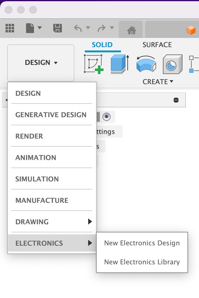
even though I know this will be on a whole new level!! Eagle is what electronics design was/is known as inside Autodesk Fusion – Fusion is always being updated so some of the older tutorial videos linked below things may be in different places but it still should work the same – for example Electronics design can now be accessed from the workspace menu in Autodesk Fusion – this just happened in a recent update.

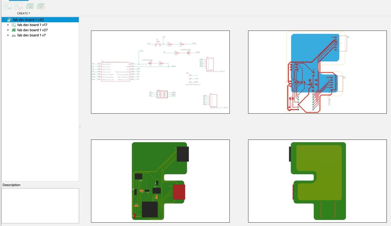
I made a variation of Adrian Torres Fab XIAO dev board as I will be working with the XIAO-RP2040 or the XIAO - ESP32 C3 in my final project – not sure which yet!! But also because I needed something to follow as I'm not really sure how to design a PCB… I need something to follow.
My first attempt.
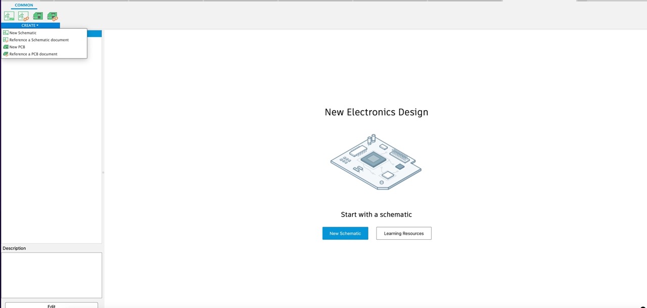
Open Autodesk Fusion – from the workspace drop down select >Electronics > New Electronics design.
 Select New Schematic
 A few new tabs will open up – I clicked new PCB in the top left.
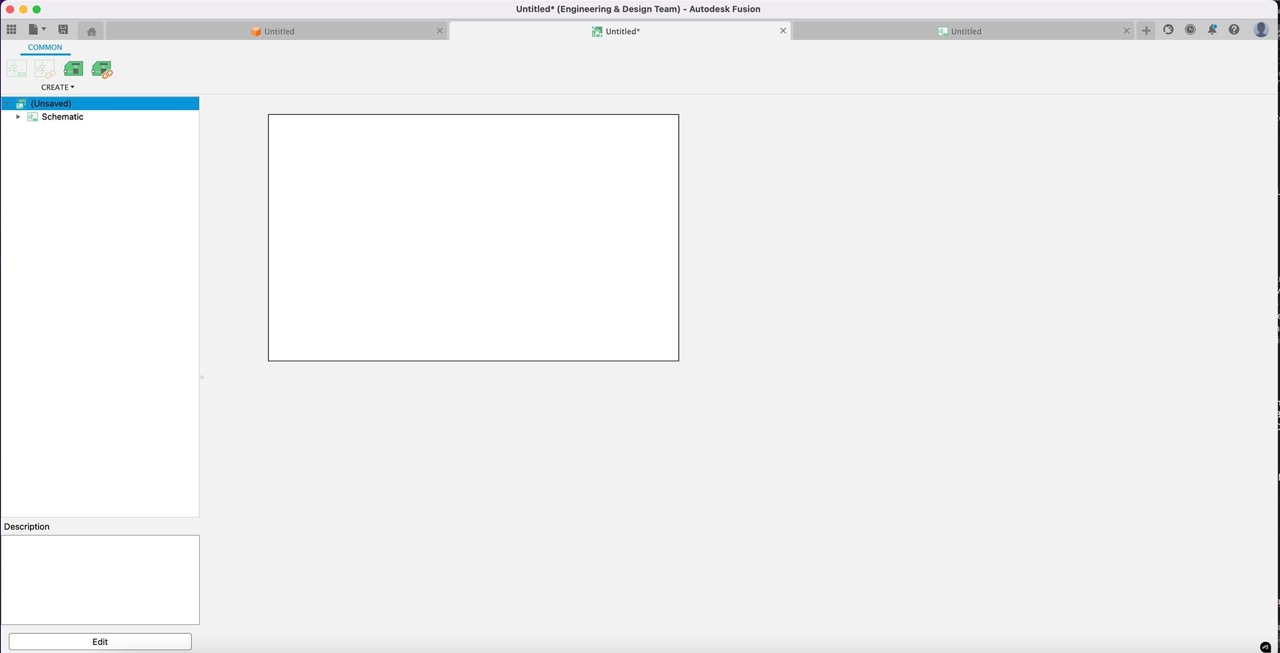
This will bring you into a new Tab – there will be a lot of jumping between tabs here and it can get a little frustrating..
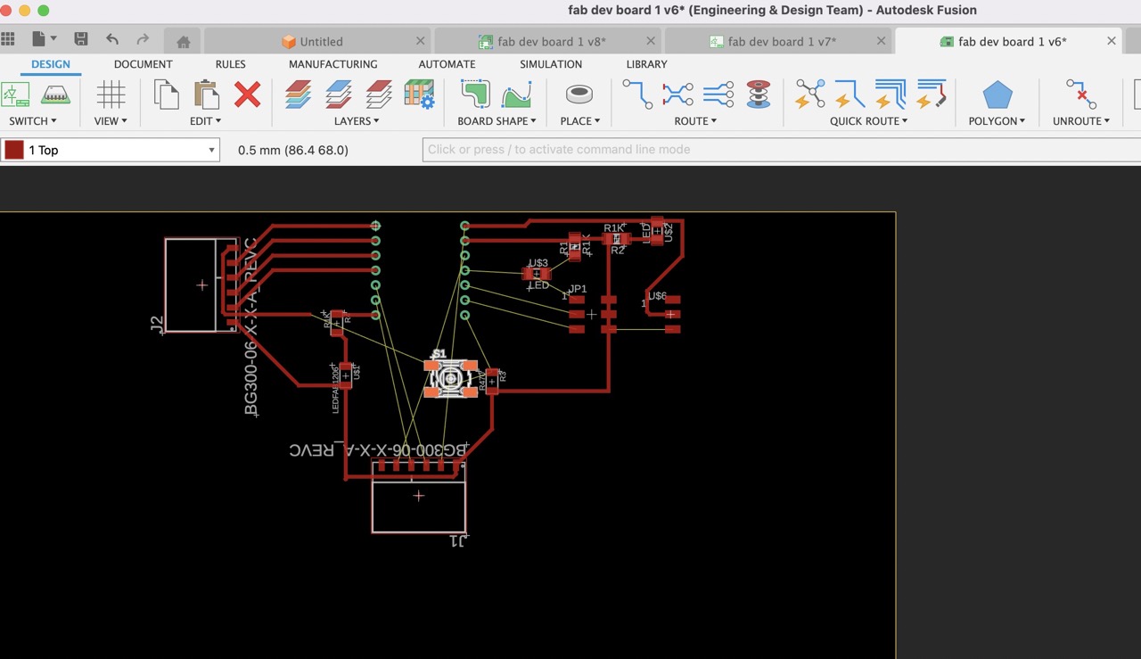
 With the Fab Library, I started adding components to the schematic and came up with the following – note you don’t need to join each net – naming them will associate them in the PCB layout. This is handy to keep the schematic neat however, it dose lead to an absolute rats nest that needs to be figured out later…
 TIP - If using the grid when placing the name annotations on the net, use the option key (on Mac) to use the finer grid snapping so the annotation sits nicely on the line.
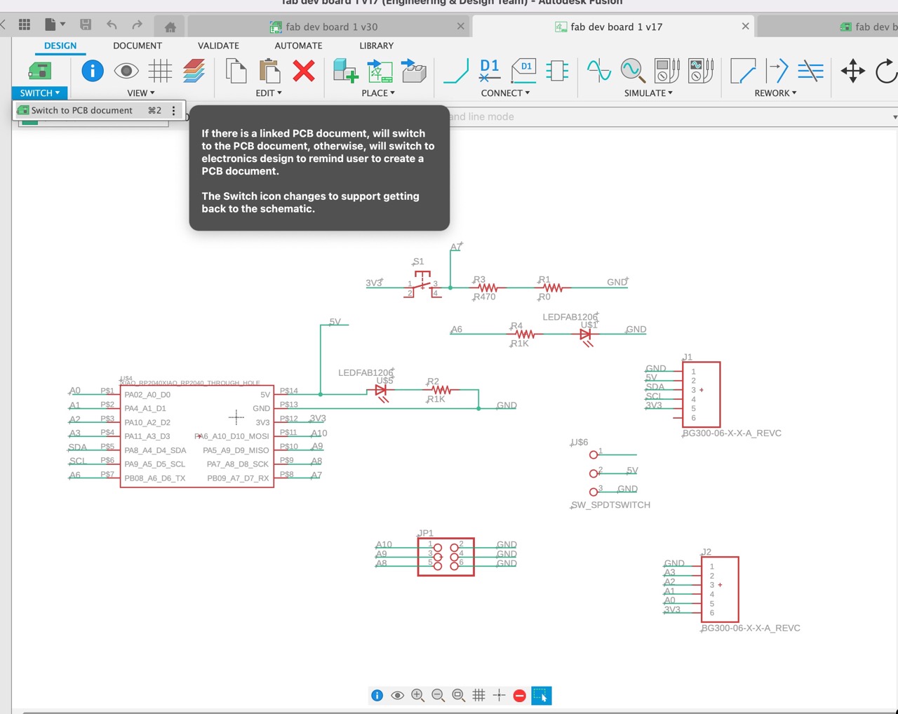
Click on switch in the top left to PCB Document to sort this rats’ nest out.
TIP - If using the grid when placing the name annotations on the net, use the option key (on Mac) to use the finer grid snapping so the annotation sits nicely on the line.
Click on switch in the top left to PCB Document to sort this rats’ nest out.
 I started putting some kind of order on parts copying Adrians layout
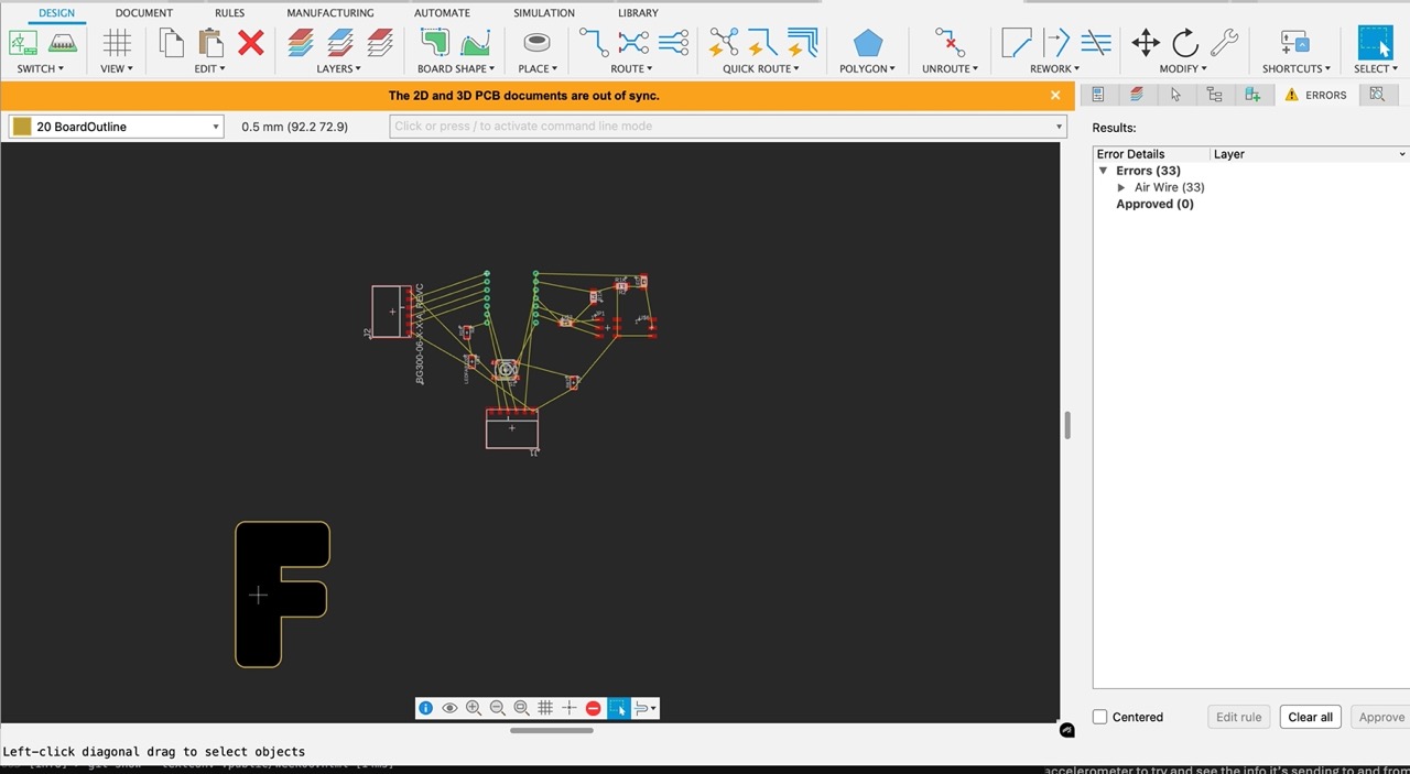
 I had the electronics bit done and routed as best I could, but there were still some unconnected routing wires. But - not wanting to copy Adrian's board completely. I did want to create a custom shape. I went with an F for Fab, so I'll call this my Fab board.
I drew an F in a new design workspace tab.
I had the electronics bit done and routed as best I could, but there were still some unconnected routing wires. But - not wanting to copy Adrian's board completely. I did want to create a custom shape. I went with an F for Fab, so I'll call this my Fab board.
I drew an F in a new design workspace tab.
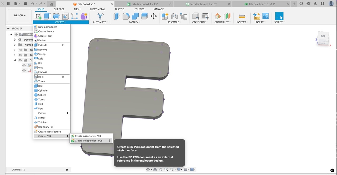
After creating the PCB design workspace, in the Create tap, select Create PCB – I think I selected Create associative PCB – Select the design you want it associated with, and it will then push it to the electronics design tabs.
 So after lots of futtering about trying to get the routing sorted I decided I should give up making a one sided board and go for a full plate of ground on the bottom face – this would save a lot time trying to route traces… and loads of 0k resistors to pass under…
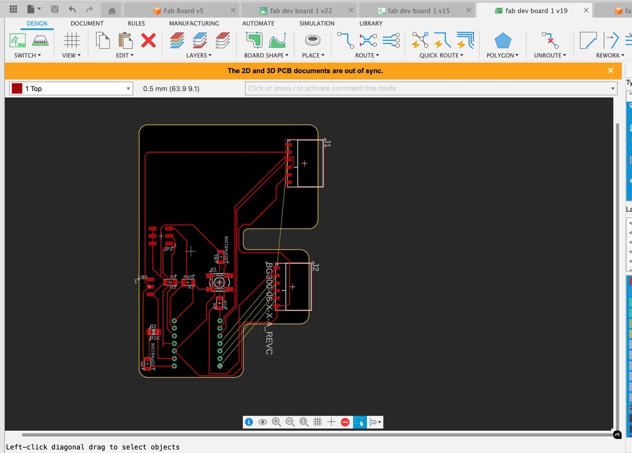 Just need to figure this out now….
I need to add a polygon on the back layer making it the GND signal.
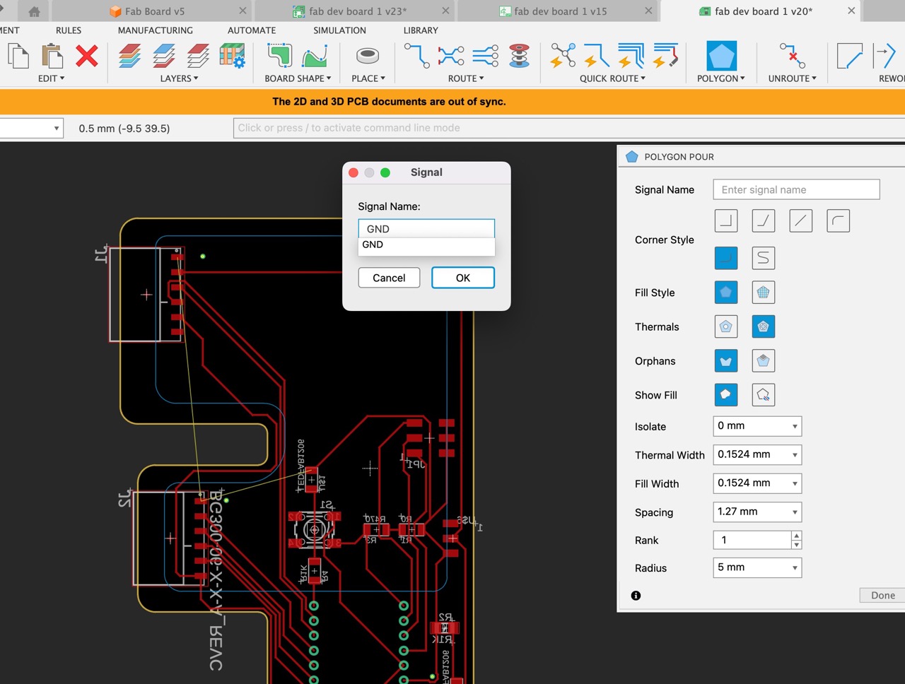
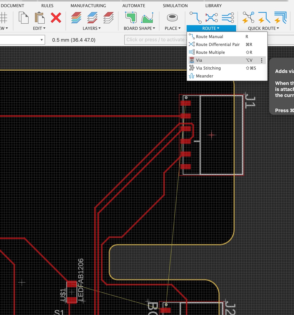
When adding a Via make sure you select a single name, in this case, GND. Otherwise, the via will be isolated from the ground net on the bottom plane.
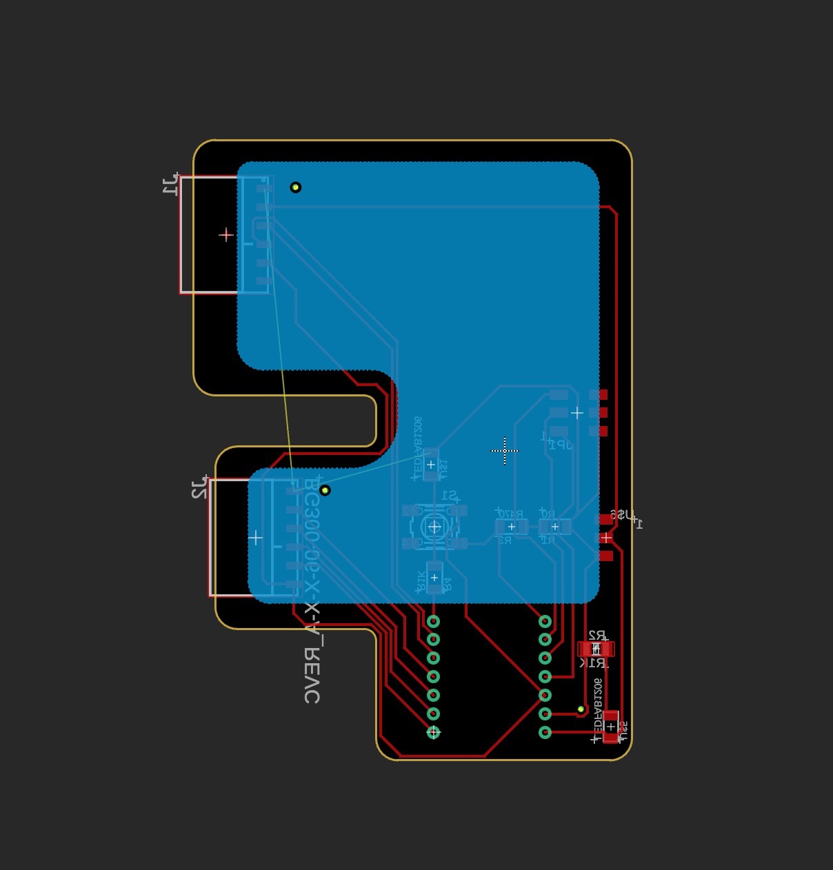
 Hopefully, this is now ready to test.
Just need to quick-route the last of the rat nest wires
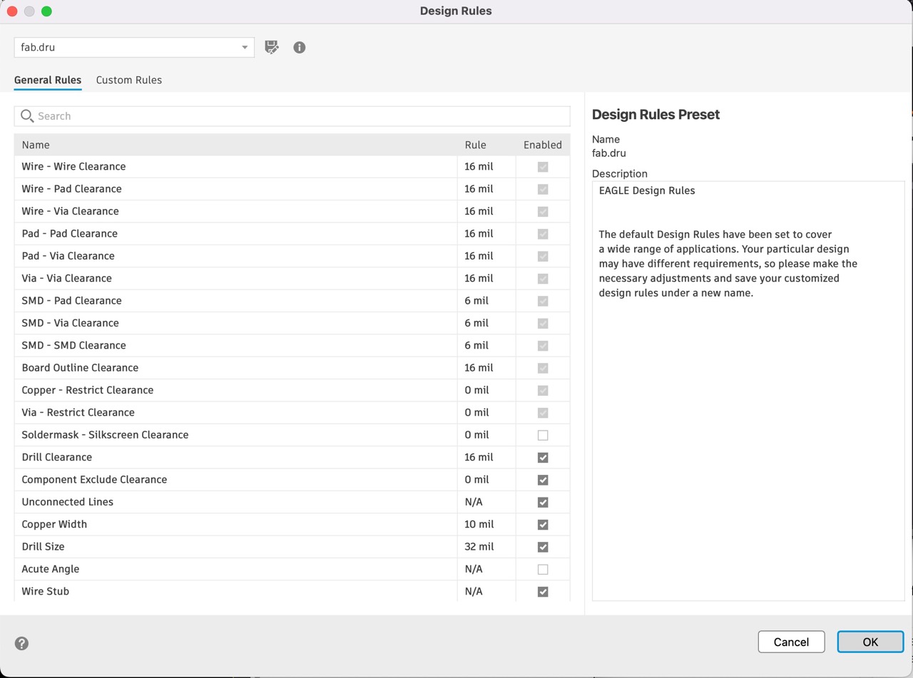
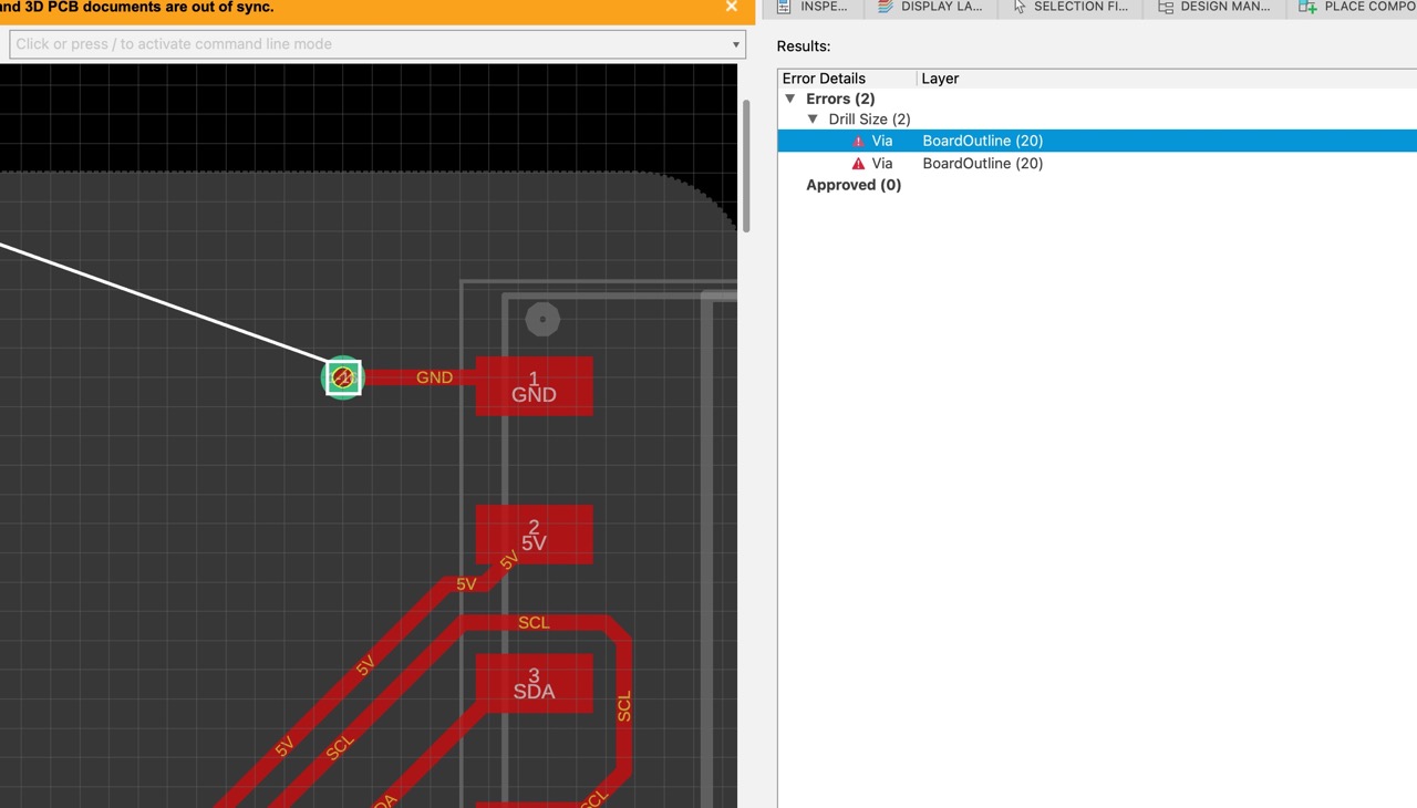
Found some errors relating to the Via holes – these did not conform to our design rules
Hopefully, this is now ready to test.
Just need to quick-route the last of the rat nest wires
Found some errors relating to the Via holes – these did not conform to our design rules
 These had to be adjusted – right-click on the component and select properties.
Change to through hole to 8.5mm in order to comply with our design rules.
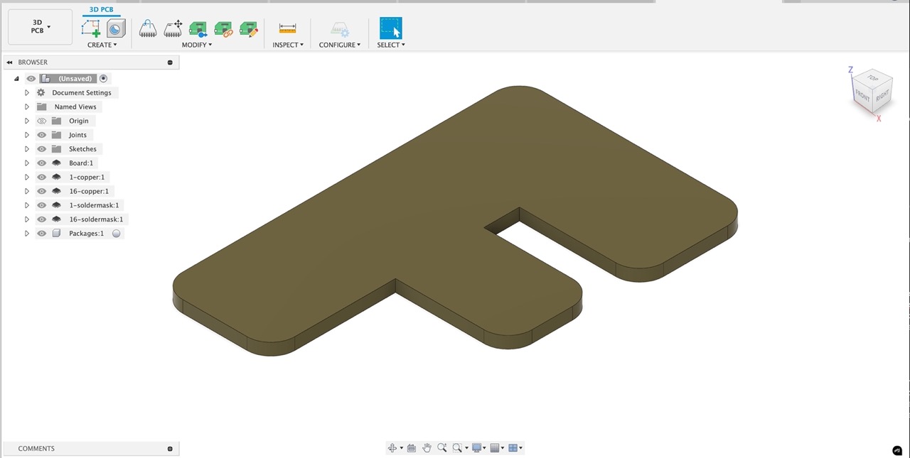
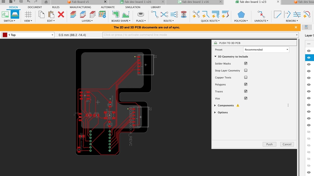
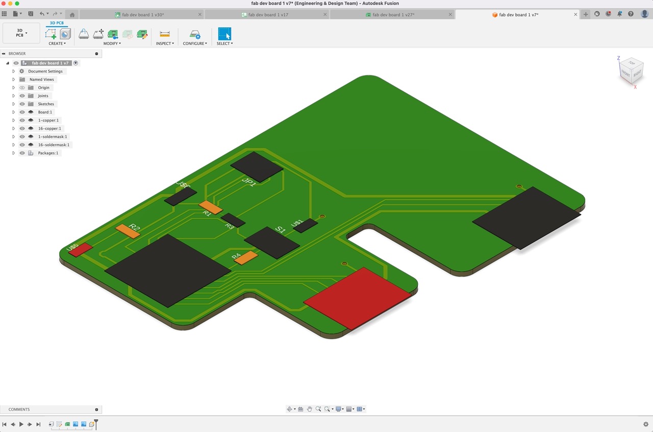
I could now push the model to 3d PCB in the top left – don’t forget to save!!
These had to be adjusted – right-click on the component and select properties.
Change to through hole to 8.5mm in order to comply with our design rules.
I could now push the model to 3d PCB in the top left – don’t forget to save!!
 I also realised that the traces are very thin – so I upped them a little larger for the Power than the others.
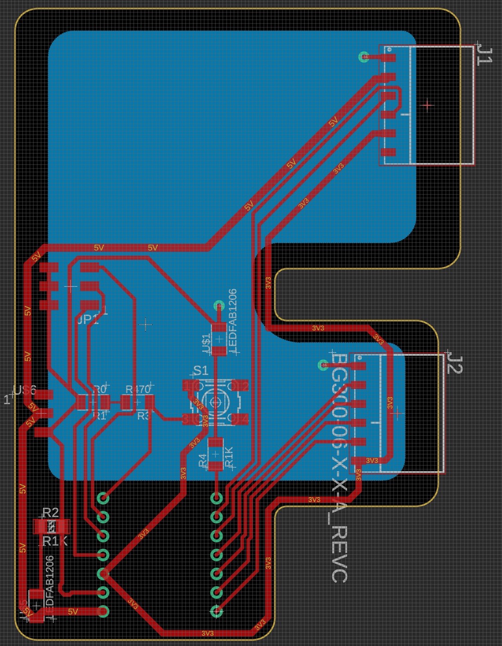 I used Cmd + Shift on Mac to select all the traces I wanted, then adjusted the thickness. ( in fairness, this will probably need to change again)
I pushed to 3d PCB board but
I seem to be missing the 3d models for the design library – this appears when pushing the from the 2d PCB to the 3D PCB.
I used Cmd + Shift on Mac to select all the traces I wanted, then adjusted the thickness. ( in fairness, this will probably need to change again)
I pushed to 3d PCB board but
I seem to be missing the 3d models for the design library – this appears when pushing the from the 2d PCB to the 3D PCB.
 Let’s fix that…
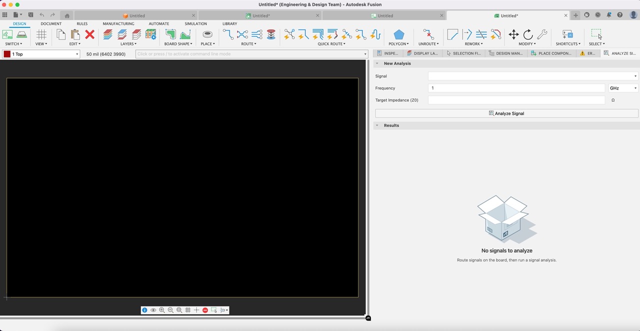
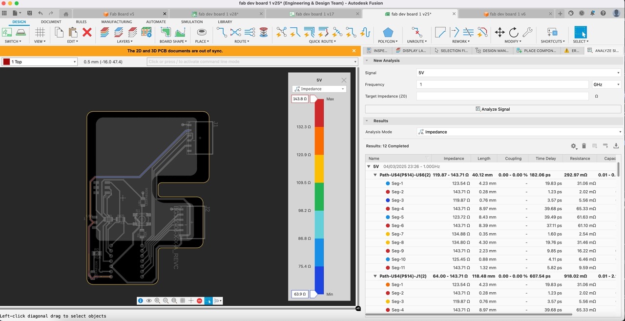
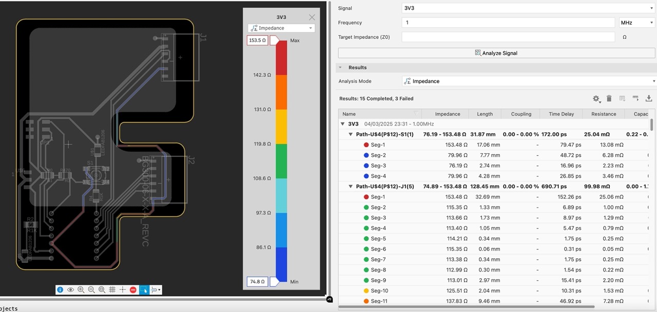
But first, I tried to run some simulations – looks like it’s just signal analysis in fusion – honestly, I have no idea what I'm doing here but here are some initial screen shots… I’ll figure this out over the coming weeks I guess, after I’ve caught up on everything else that I'm falling behind on
Let’s fix that…
But first, I tried to run some simulations – looks like it’s just signal analysis in fusion – honestly, I have no idea what I'm doing here but here are some initial screen shots… I’ll figure this out over the coming weeks I guess, after I’ve caught up on everything else that I'm falling behind on

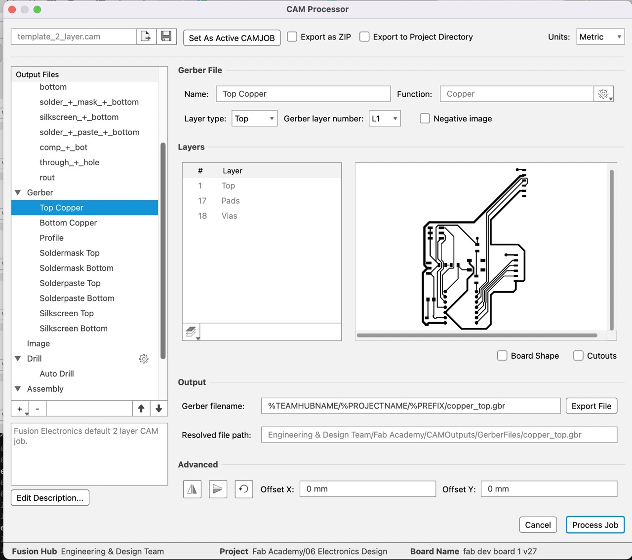
Exporting the Gruber files for milling… let’s try to figure this out!!
Selected the manufacture tab (within 2d PCB layout) Select1. the cam preview button
2. then select each button at the bottom 2, 3, and 4 first two export DXF and PNG respectively the CAM button will be
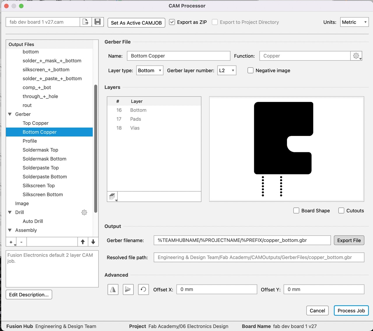
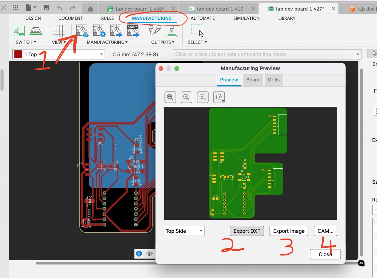 1. Under the CAM section, we can export the Gerber files that are needed –
You can select each of the parts.
1. Under the CAM section, we can export the Gerber files that are needed –
You can select each of the parts.
 And hit save job as in the to left
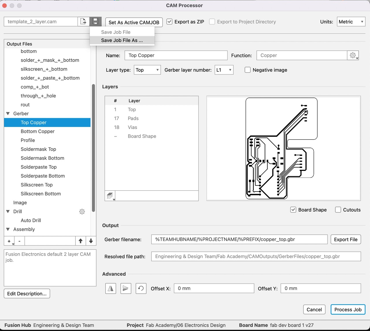
That didn’t work so I selected export in the bottom right
Think that will export separate files.
 But to get the entire archive in zip format (make sure zip is ticked at the top
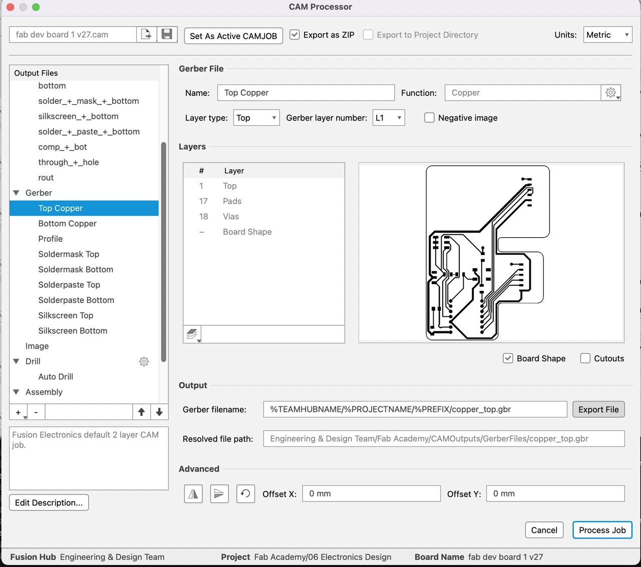
Select the upper Level Gerber
And press process in the bottom right.
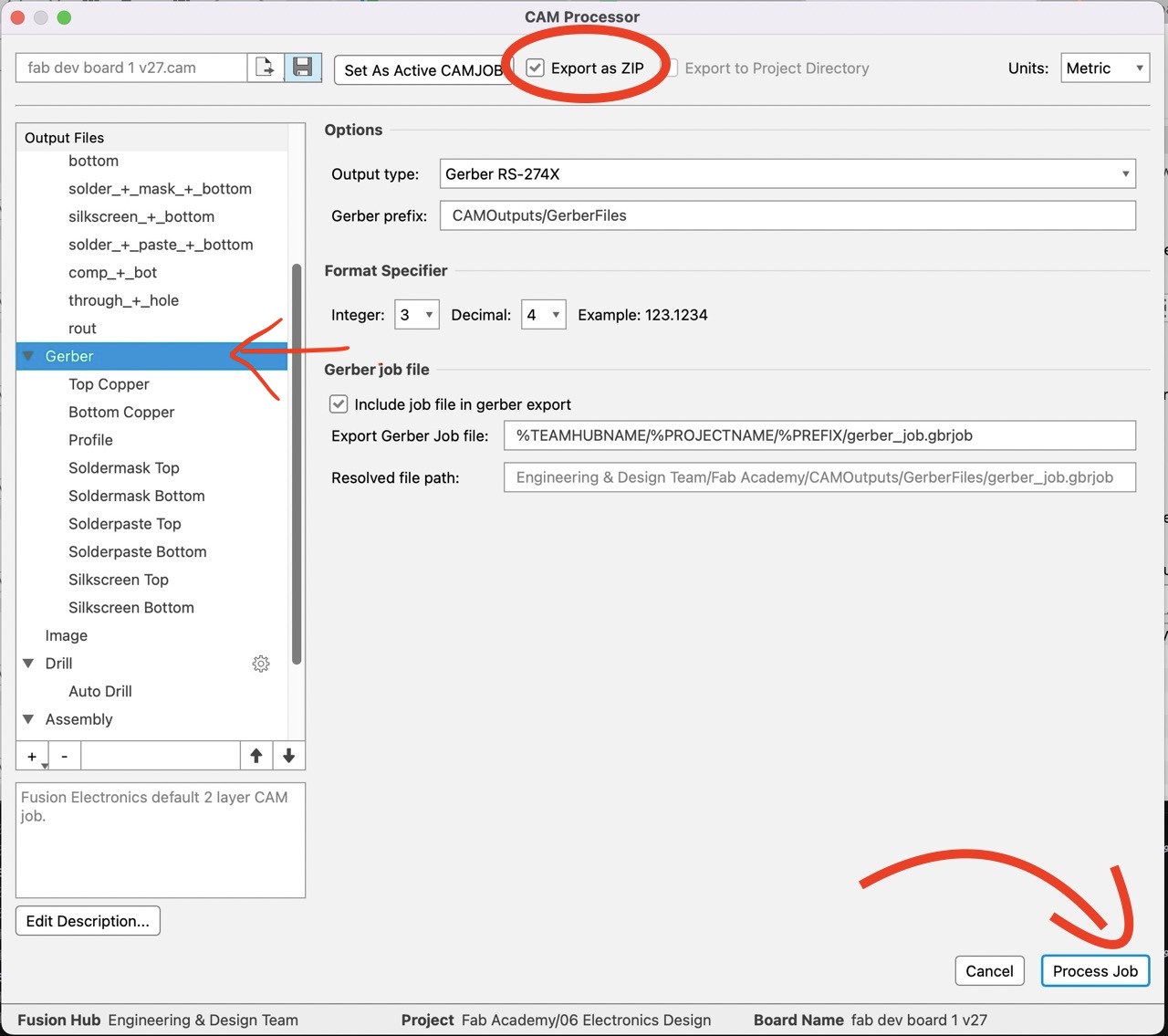
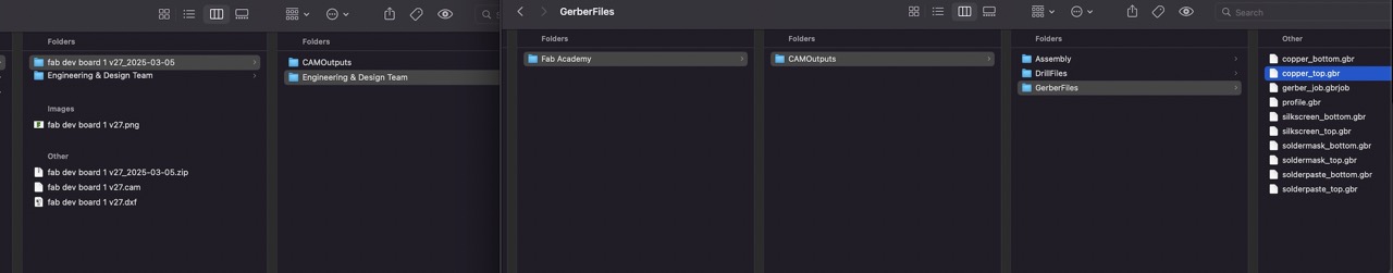
Zip archive will be saved to the selected folder – I must have selected this earlier – make sure it is going somewhere you can find it – Fusion has a habit of sending files to some buried folder you might never find…
Issues I’ve encountered
AGHHHHH
Too many to mention….Very frustrating getting the hang of electronics design with a lot of jumping between tabs, - 2d and 3d views and pushing parts to and from these.
There is a significant amount of information overload in the various menus that can make it difficult to find things – persistence is key. It’s quite rewarding when you figure something out for yourself is quite key!!.
Learning Outcomes
a lot about PCB design and how to use Eagle to design a PCB.