Weekly assignments
- week 1. Project Management
- week 2. Computer Aided Design
- week 3. Computer Controlled Cutting
- week 4. Electronics Production
- week 5. 3D Scanning and Printing
- week 6. Embeded Programming
- week 7. Computer Controlled Machining
- week 8. Electronics Design
- week 9. Output Devices
- week 10. Mechanical design & Machine Design
- week 11. Break & Midterm Review
- week 12. Input devices
- week 13. Moulding and Casting
- week 14. Networking and communications
- week 15. Interface and application programming
- week 16. Wildcard week
- week 17. Applications And implications
- week 18. Project Development
- week 19. Invention, Intellectual Property and Income
Week08. Electronic Design
Group assignment:
Individual assignment:
an embedded microcontroller, produce it, and test it
Research
PCB Design Softwares
1. Altium Designer:
Altium Designer is a comprehensive PCB design software widely used in the electronics industry.
It offers features like multi-board design, 3D PCB visualization, advanced routing capabilities, and integration with ECAD-MCAD collaboration.
Altium Designer is known for its powerful features and is often used for complex and high-density PCB designs.
2. KiCad:
KiCad is an open-source and cross-platform PCB design software.
It includes tools for schematic capture, PCB layout, 3D visualization, and design rule checking.
KiCad is a popular choice for hobbyists, small businesses, and educational institutions due to its free availability and growing community support.
3. Eagle (Autodesk Eagle):
Eagle (Autodesk Eagle) is a PCB design software known for its user-friendly interface and versatility.
It offers features like schematic capture, PCB layout, and integrated component libraries.
Autodesk Eagle has both free and paid versions, making it accessible to a wide range of users, from hobbyists to professional designers.
4. CircuitMaker:
CircuitMaker is a free, cloud-based PCB design software developed by Altium.
It provides a modern and intuitive user interface, allowing designers to create schematics, design PCBs, and collaborate with others in real-time.
CircuitMaker is a good choice for hobbyists, students, and small teams who want an accessible and feature-rich PCB design tool.
Group Assignment My Part
1. Objective:
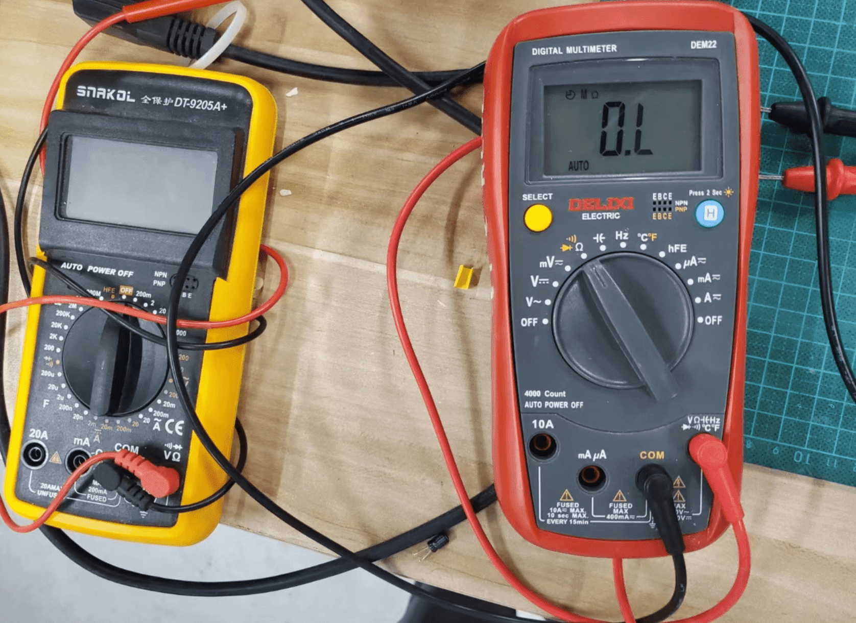
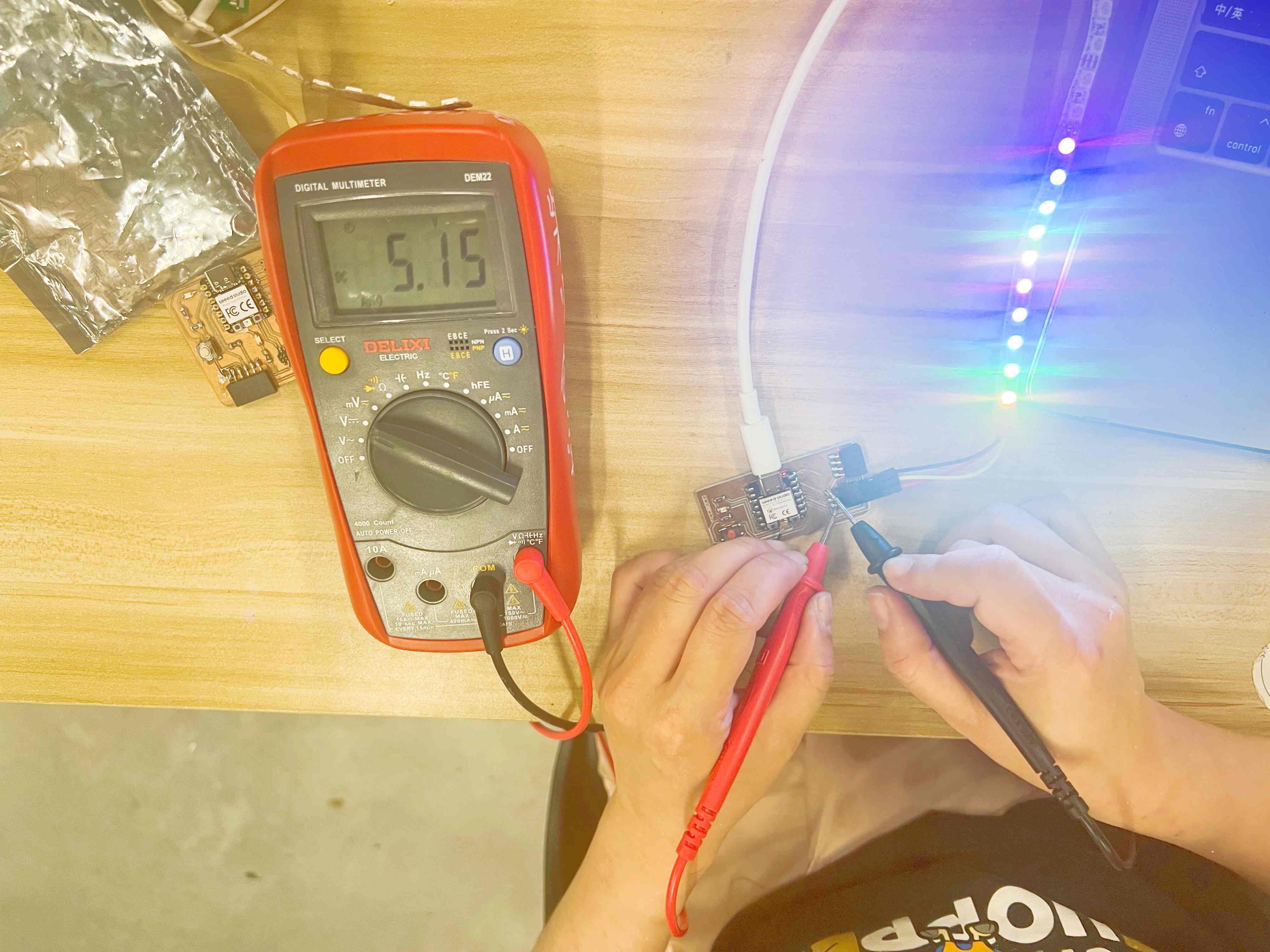
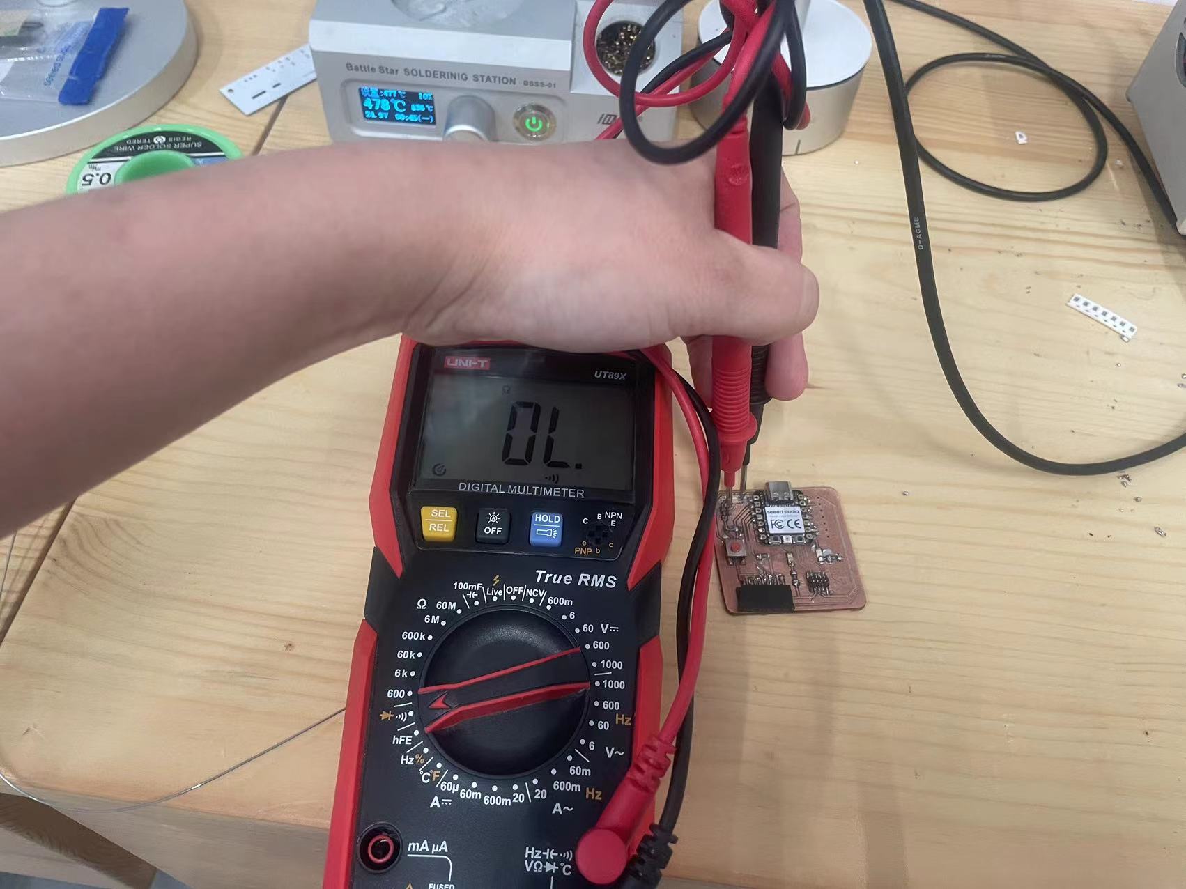
2. Equipment Used:
Multimeter Measurements:
Oscilloscope Observations:
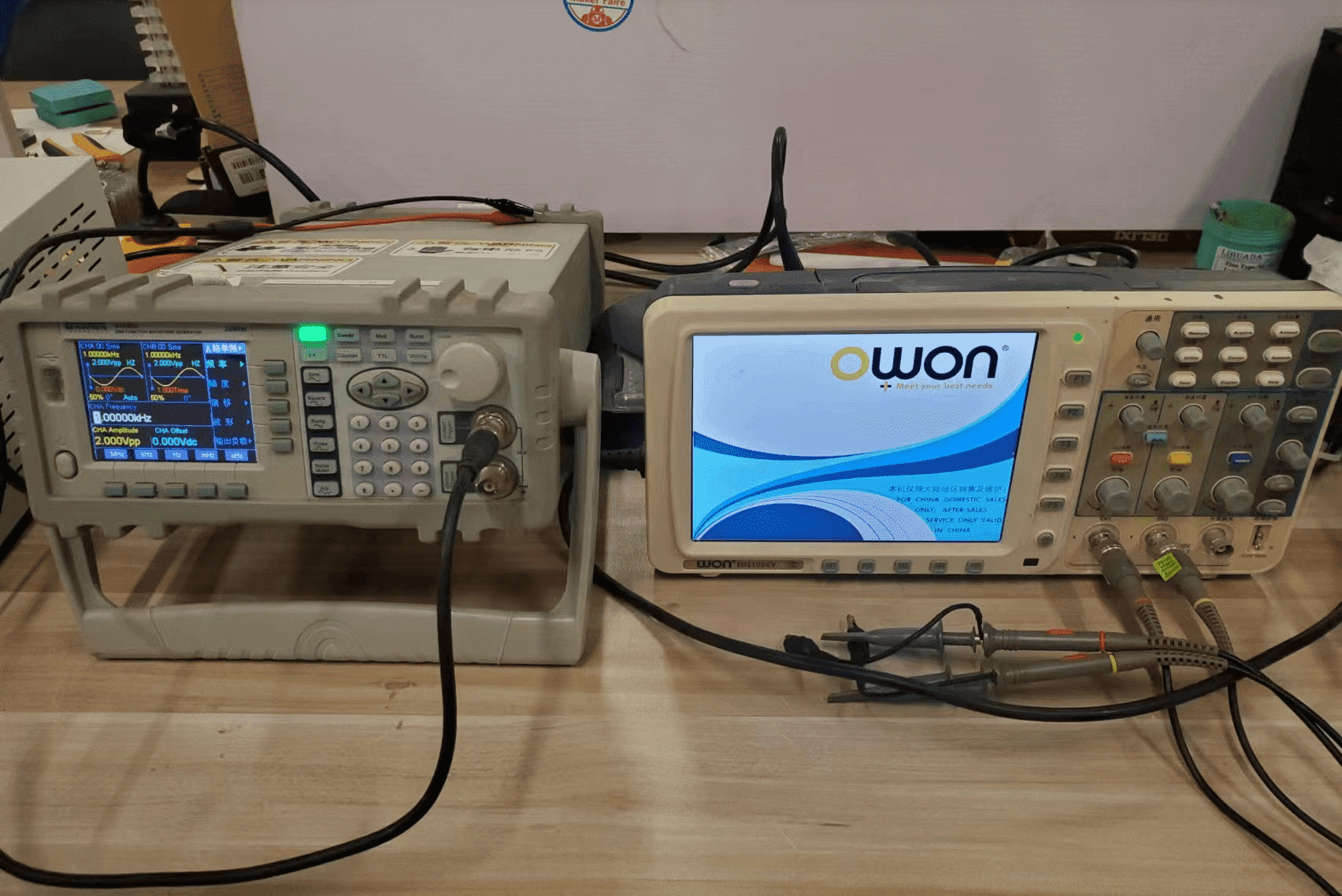
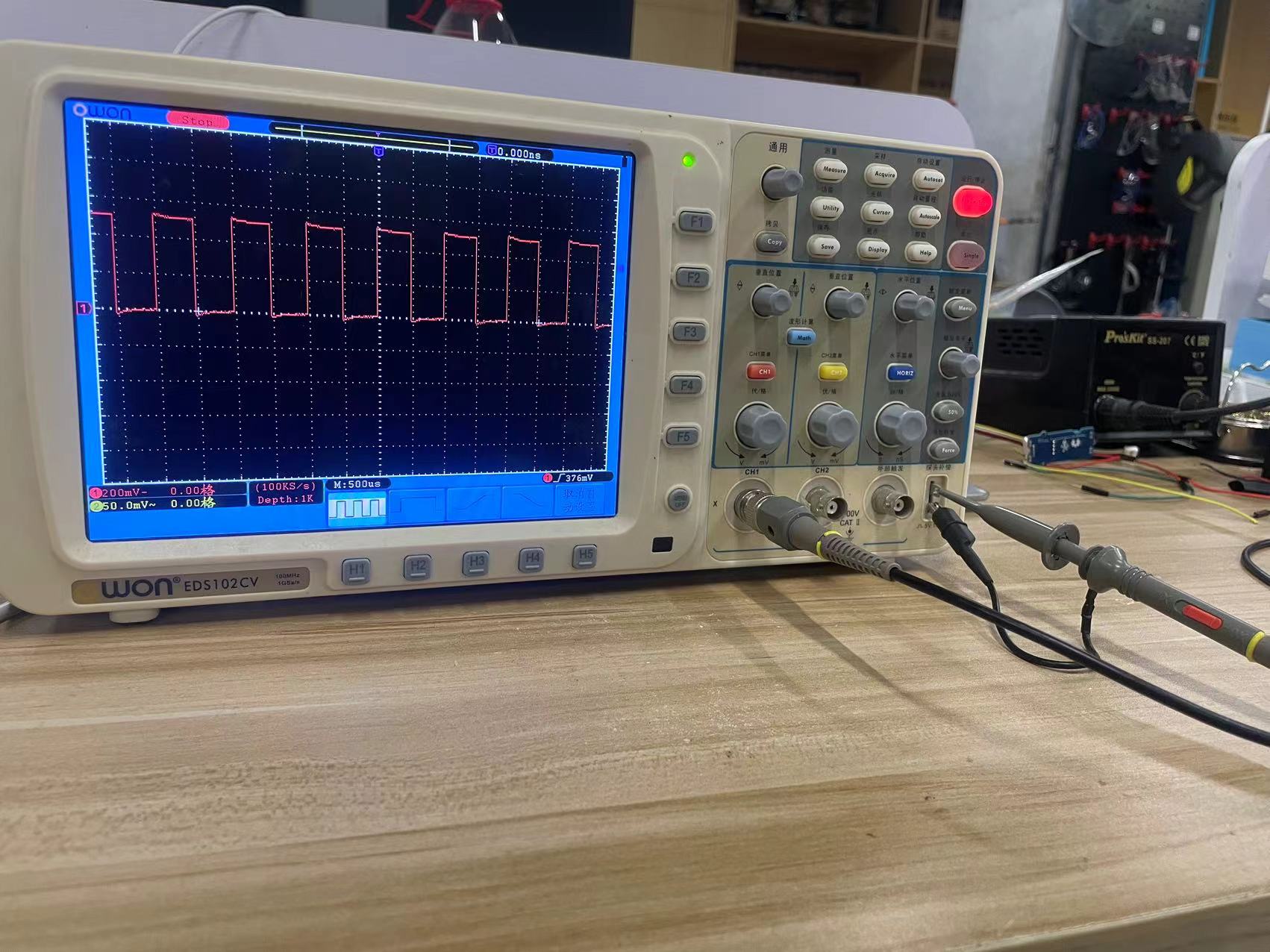
1. The oscilloscope we use is OWON EDS102CV
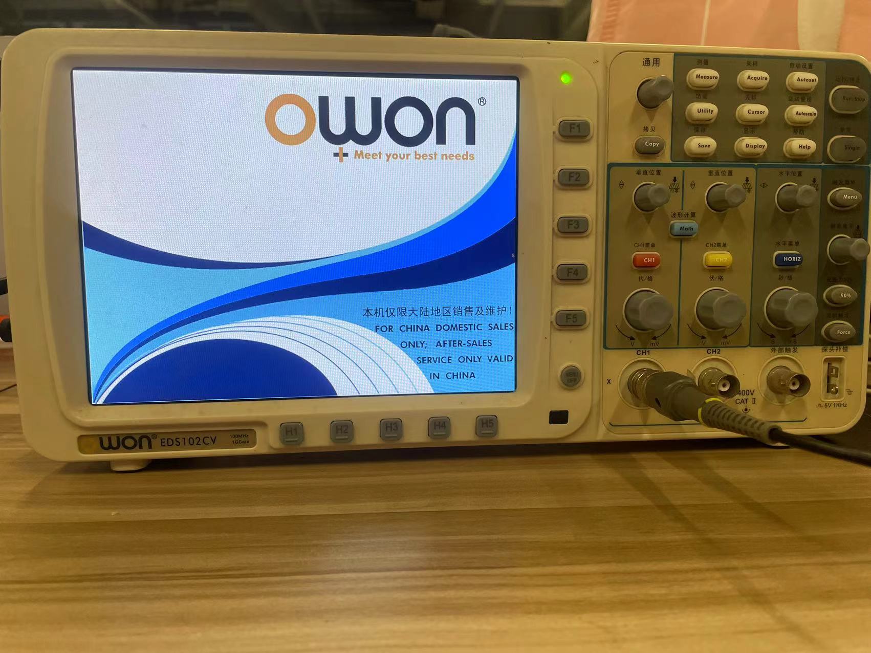
2. I read the instruction manual of this OWON EDS102CV
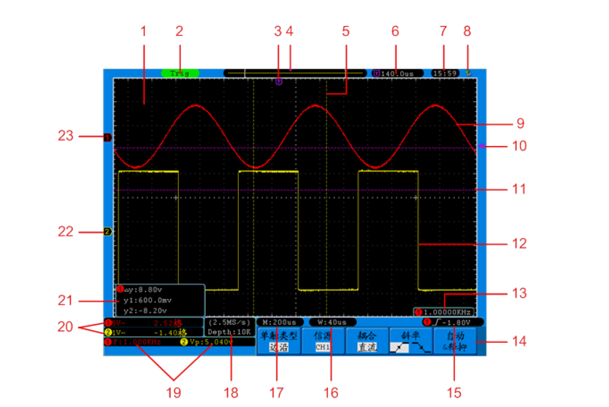
2.1 Font Panel is as below:
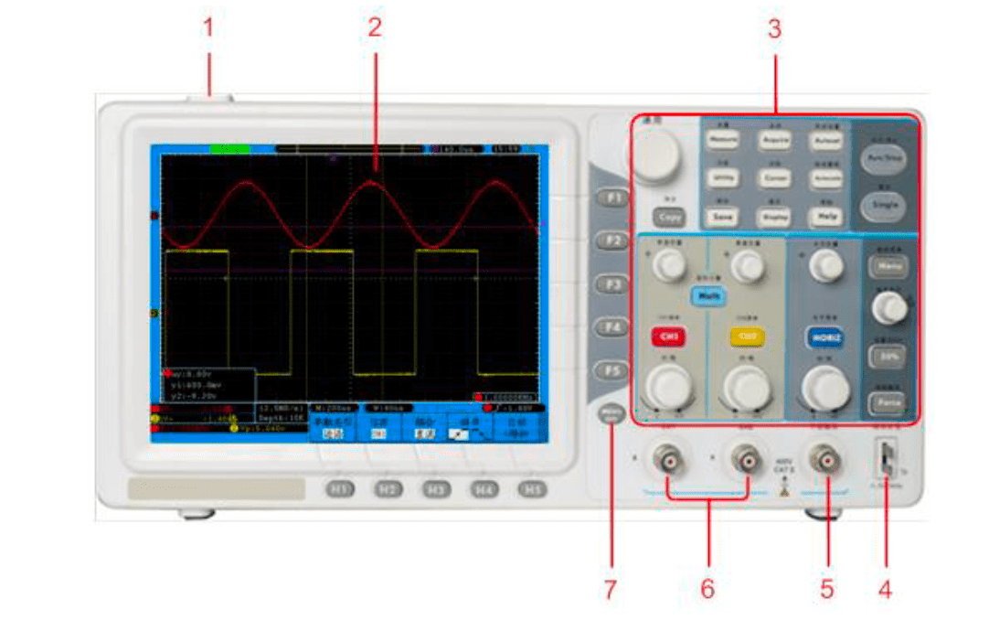
2.2 Key Control Area:
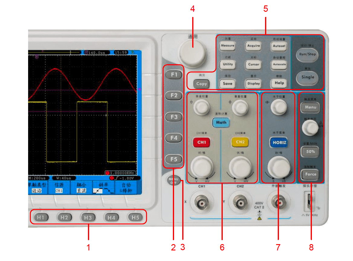
2.3 Preliminary understanding of the oscilloscope user interface
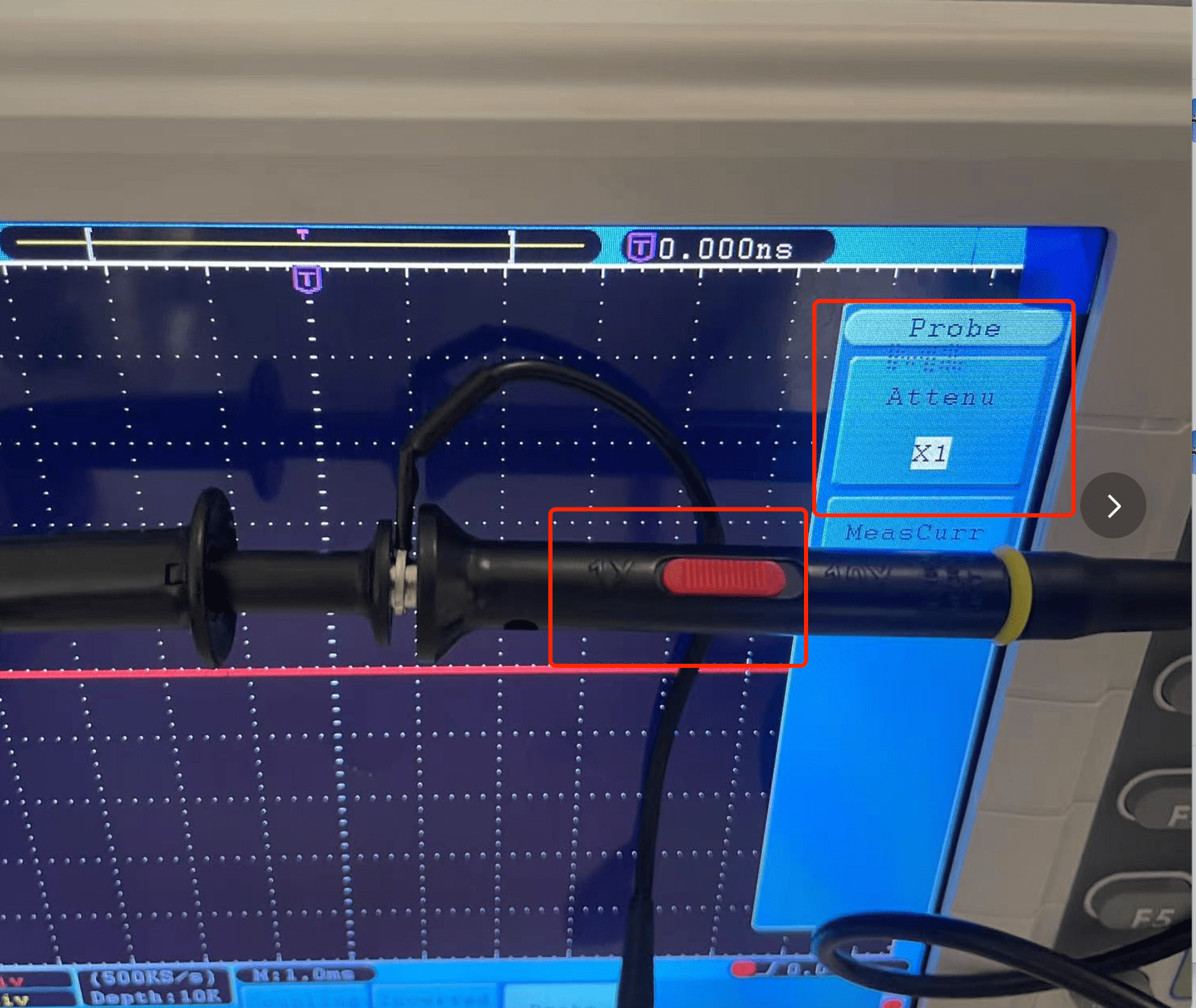
3. Conduct a functional check
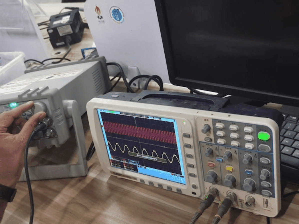
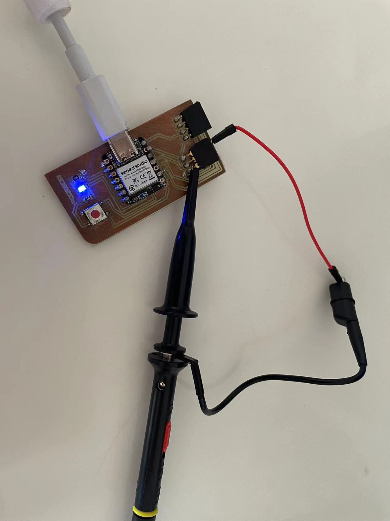
2.4 Observe the operation of a microcontroller circuit board
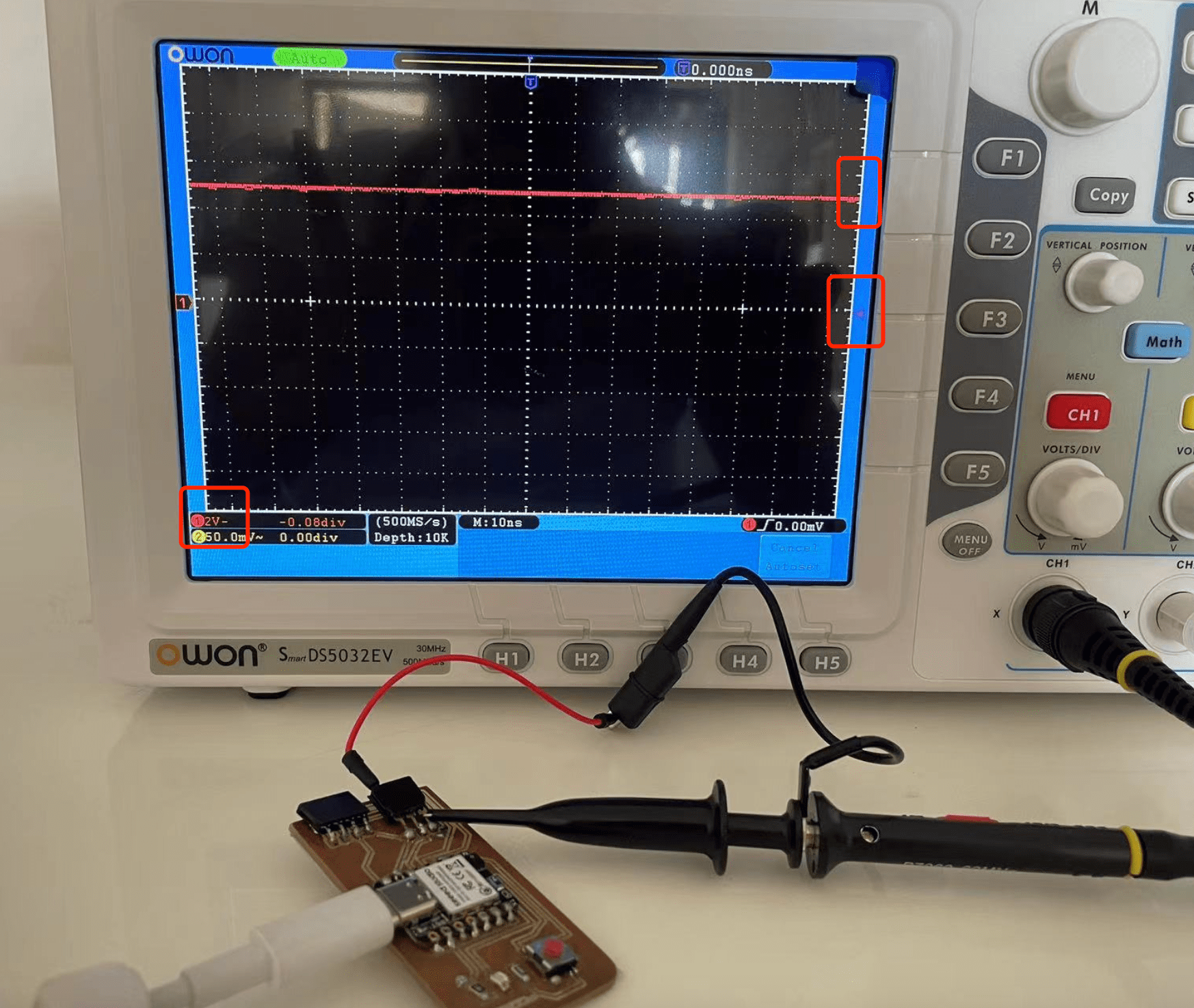
Step1. Conduct a functional check
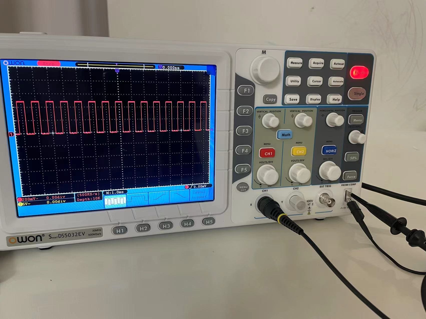
Step1. Press the trigger level button on the panel, and then press CH1 to adjust the trigger level.
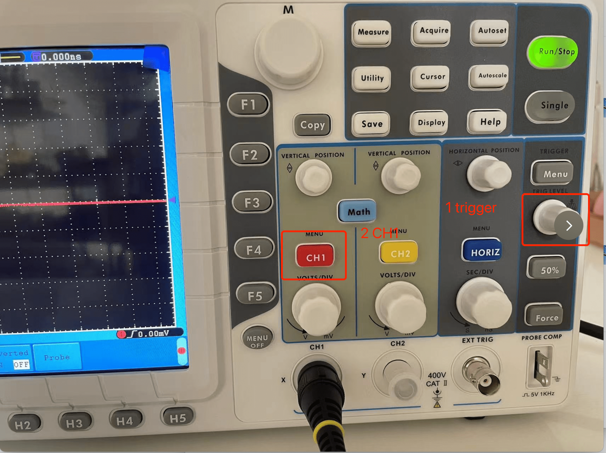
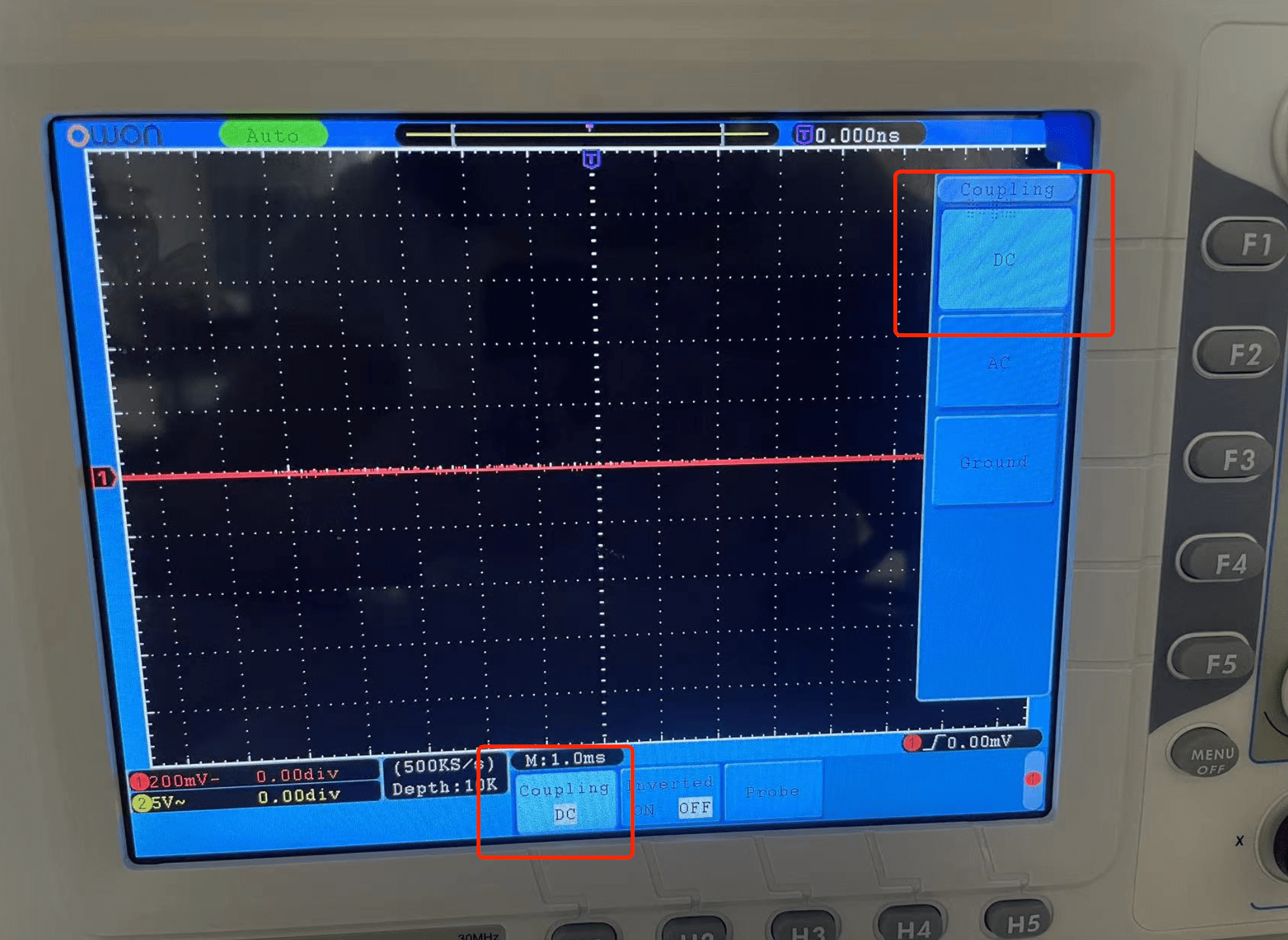
Step2. Adjust all the settings below:
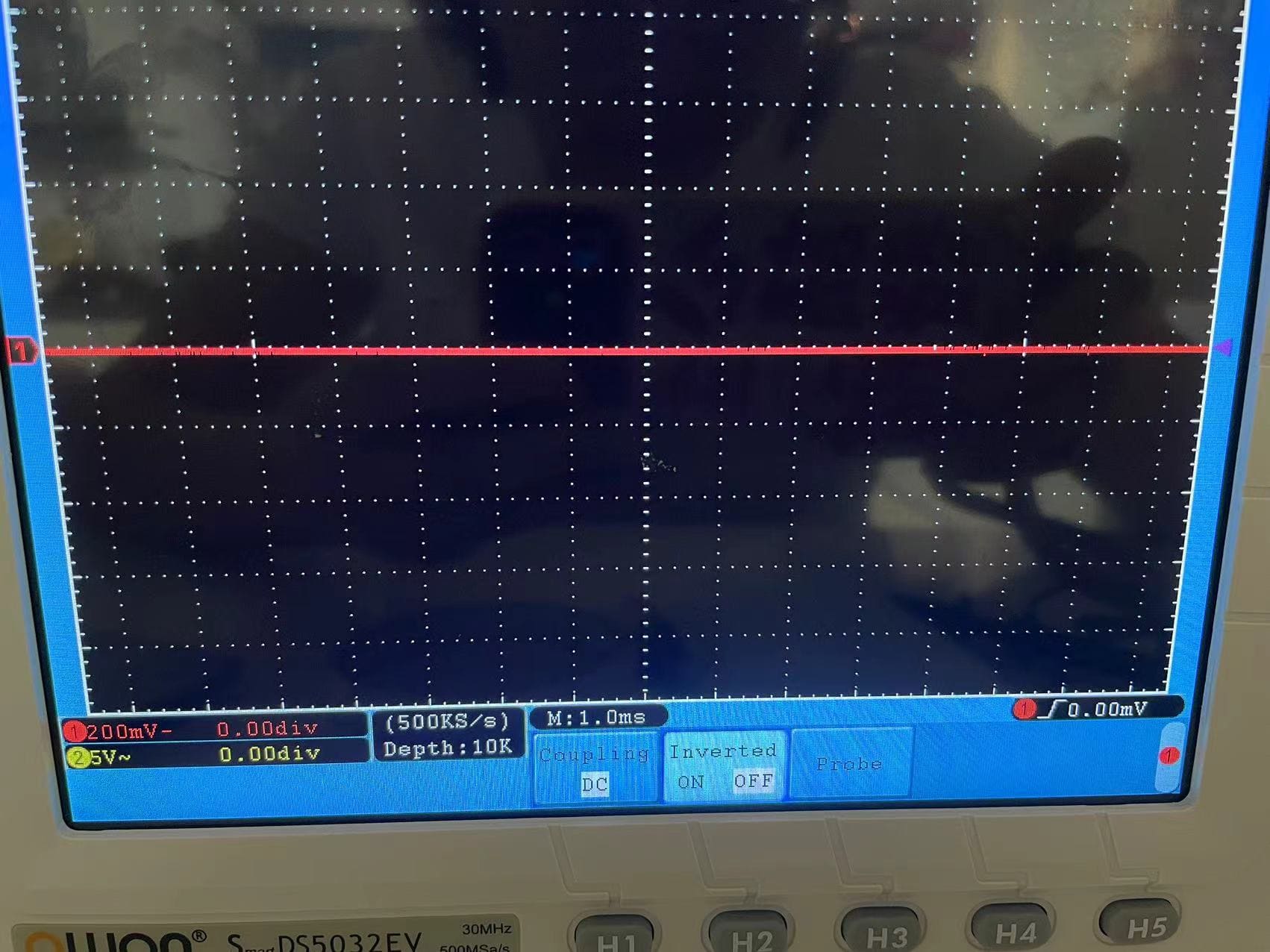
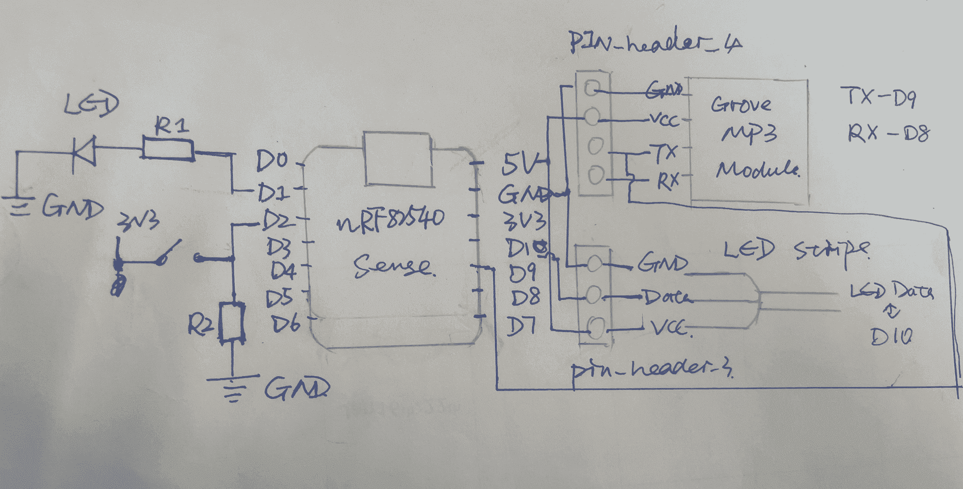
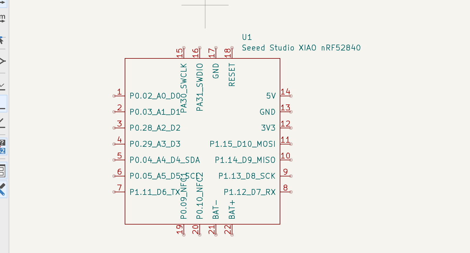
Step3. Clamp the ground wire to the ground wire of the nRF52840. Hook the signal wire to the pinheader port which is connected to nRF52840's VCC port.
Step4. The votage signal is okay!Because one grid is 2V and the voltage line is at two and half grids position above the level line, the voltage is a constant 5V.
IndividualAssignment_My PCB
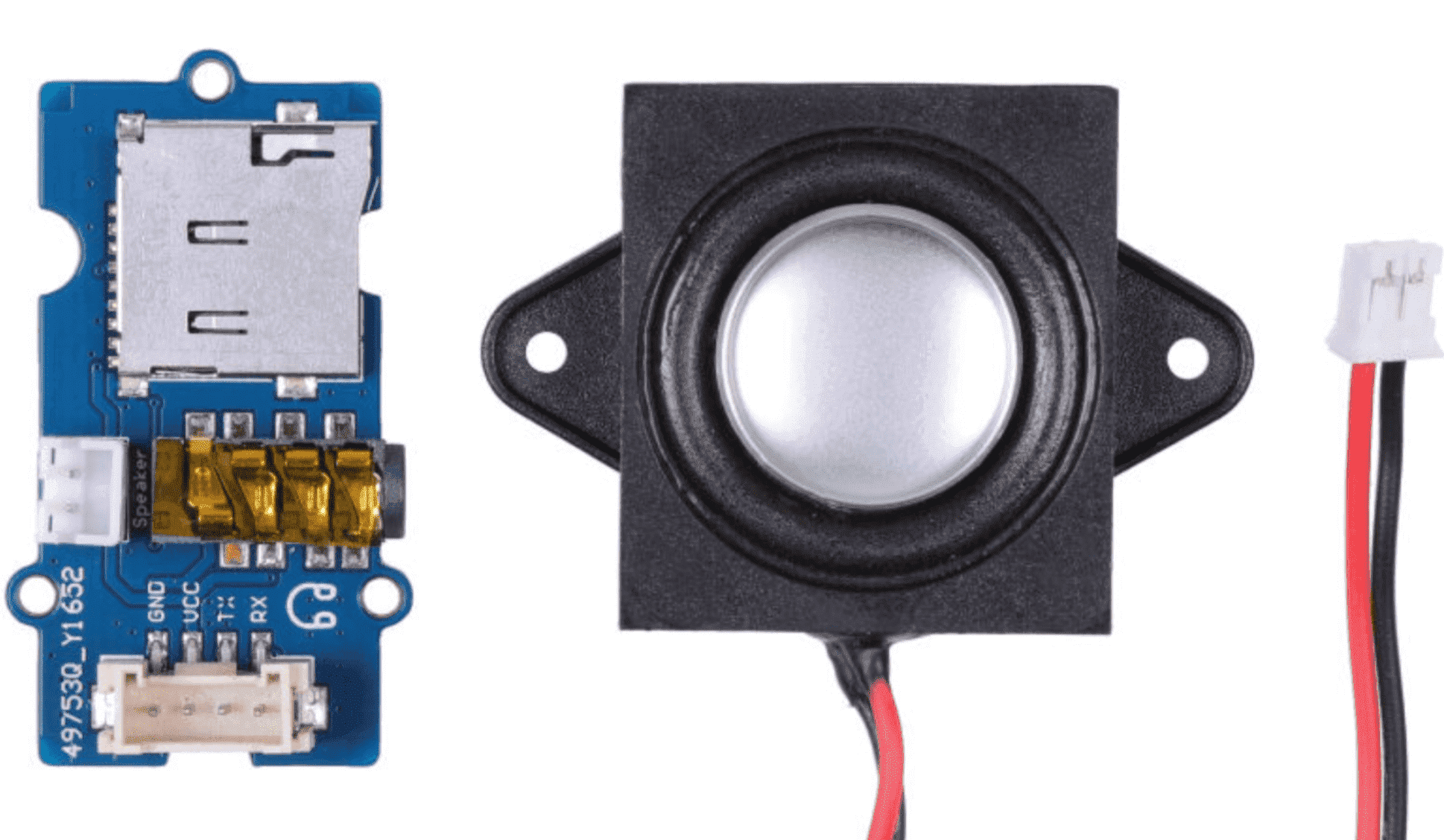
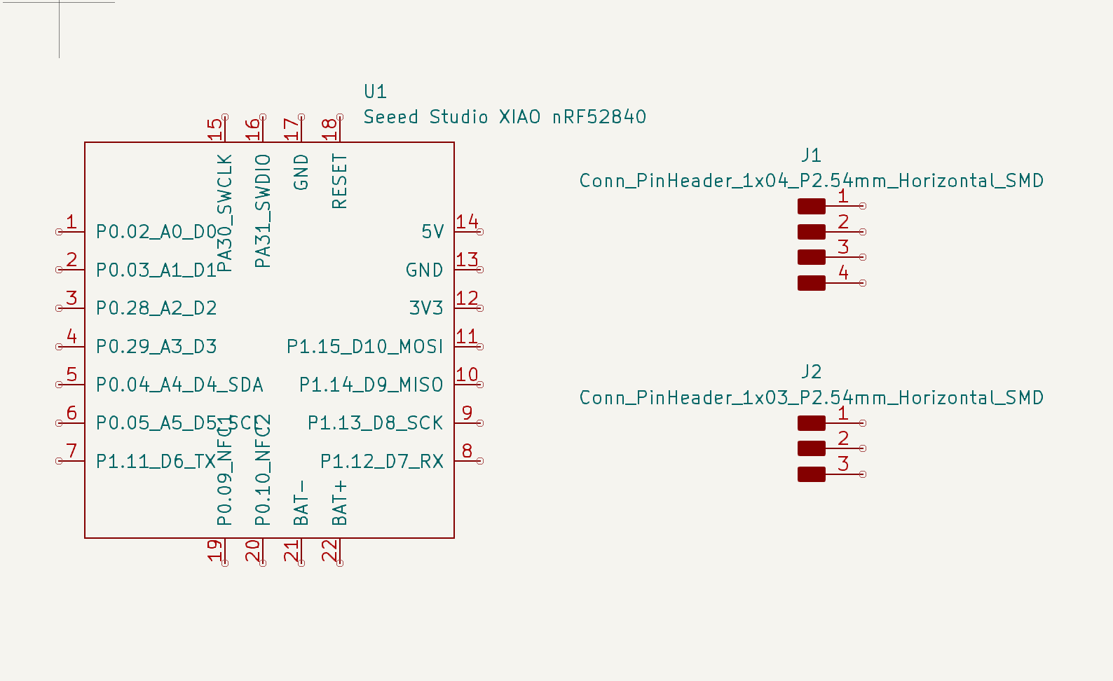
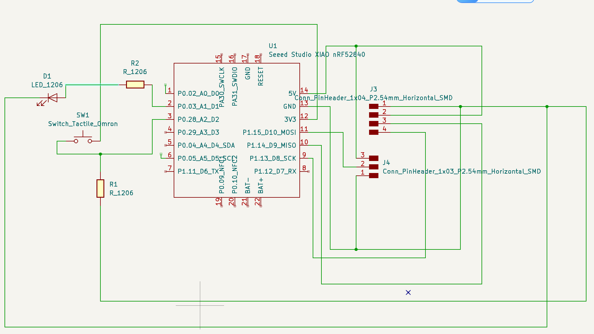
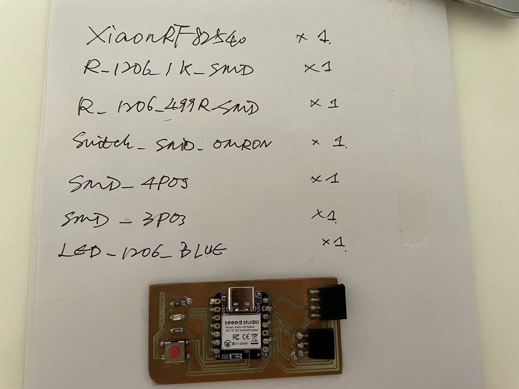
My PCB is going to use the nRF52840 chip with an IMU embedded in it, so the extra components I will use are a LED strip and a sound module in potential. It is also always helpful to add a switch and LED on your PCB for basic testing.
It is better to decide the pin connections before design of PCB schematic.
PCB Design Procedures
The basic steps of producing a PCB are: 1. Create Schematic 2. Create Board Design 3. Generate Gerber 4. Convert Gerber to PNG 5. Convert PNG to GCode 6. CNC Mill the board
Step1 Read the datasheet of the components And make a circuit Design
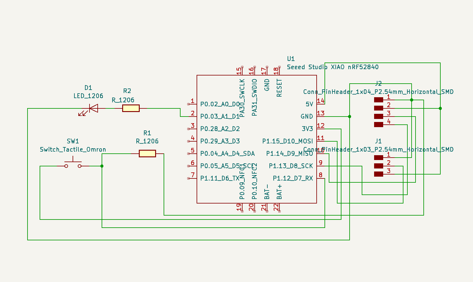
For my PCB, I will include the nRF52840 chip, a LED strip, and a Grove - MP3 Module V4.0 as peripherals, as well as a switch and an LED for basic testing.
Step2 Use KiCad to Create Schematic
First, create a project by clicking File->CreateNewProject
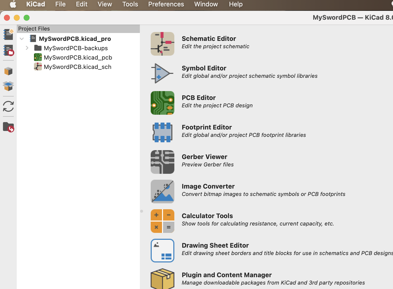
Second, click on the "***.sch" file to start editing your schematic
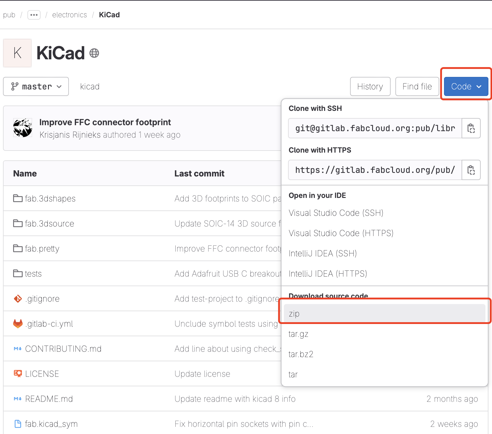
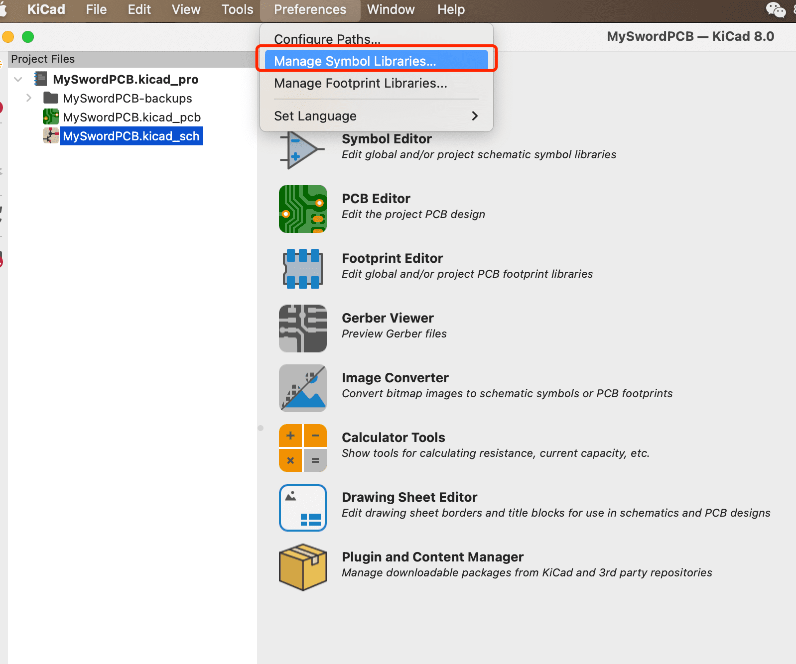
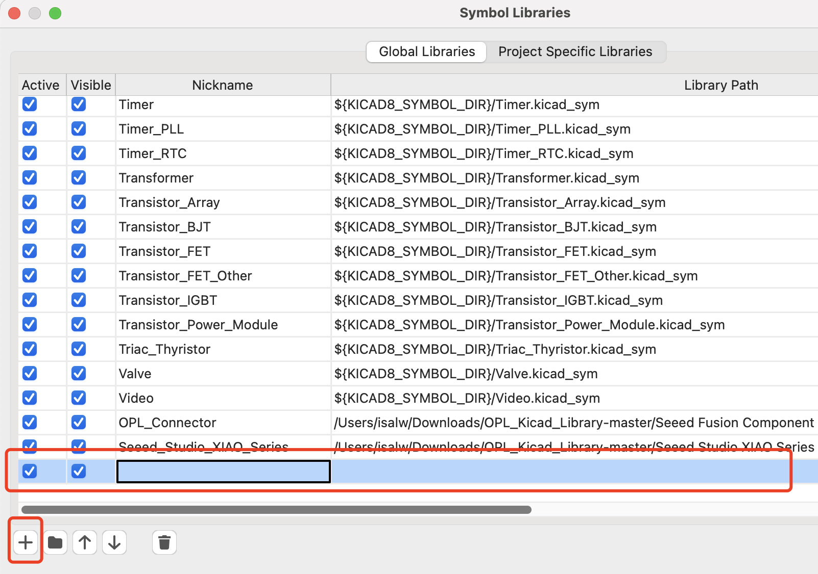
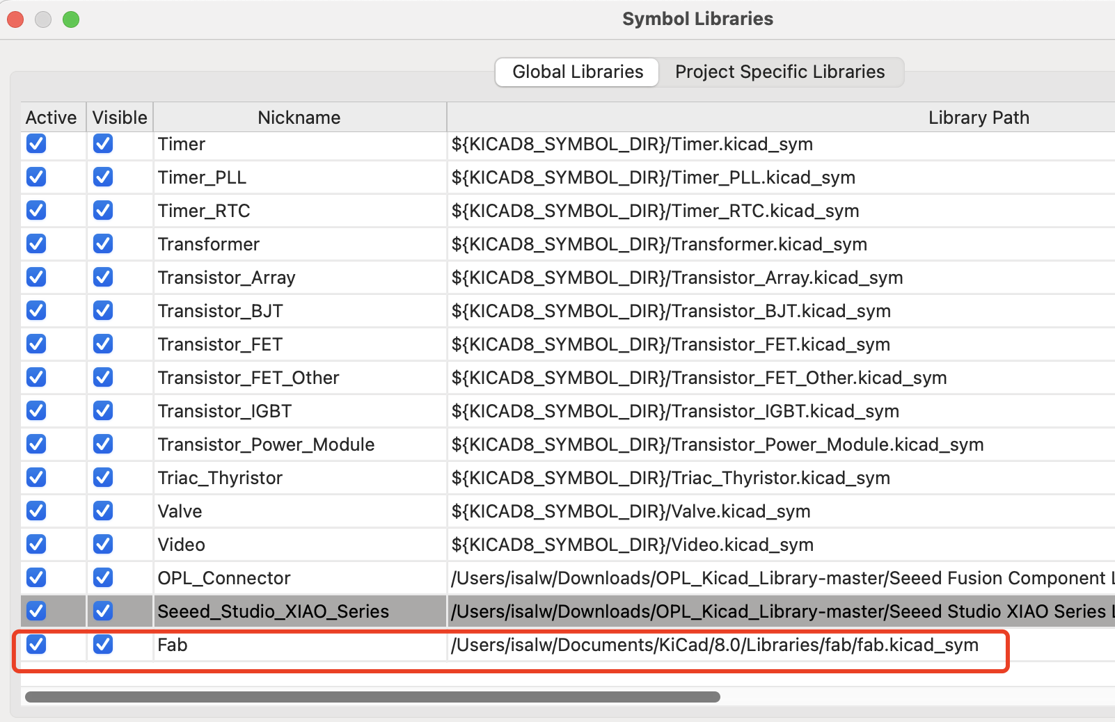
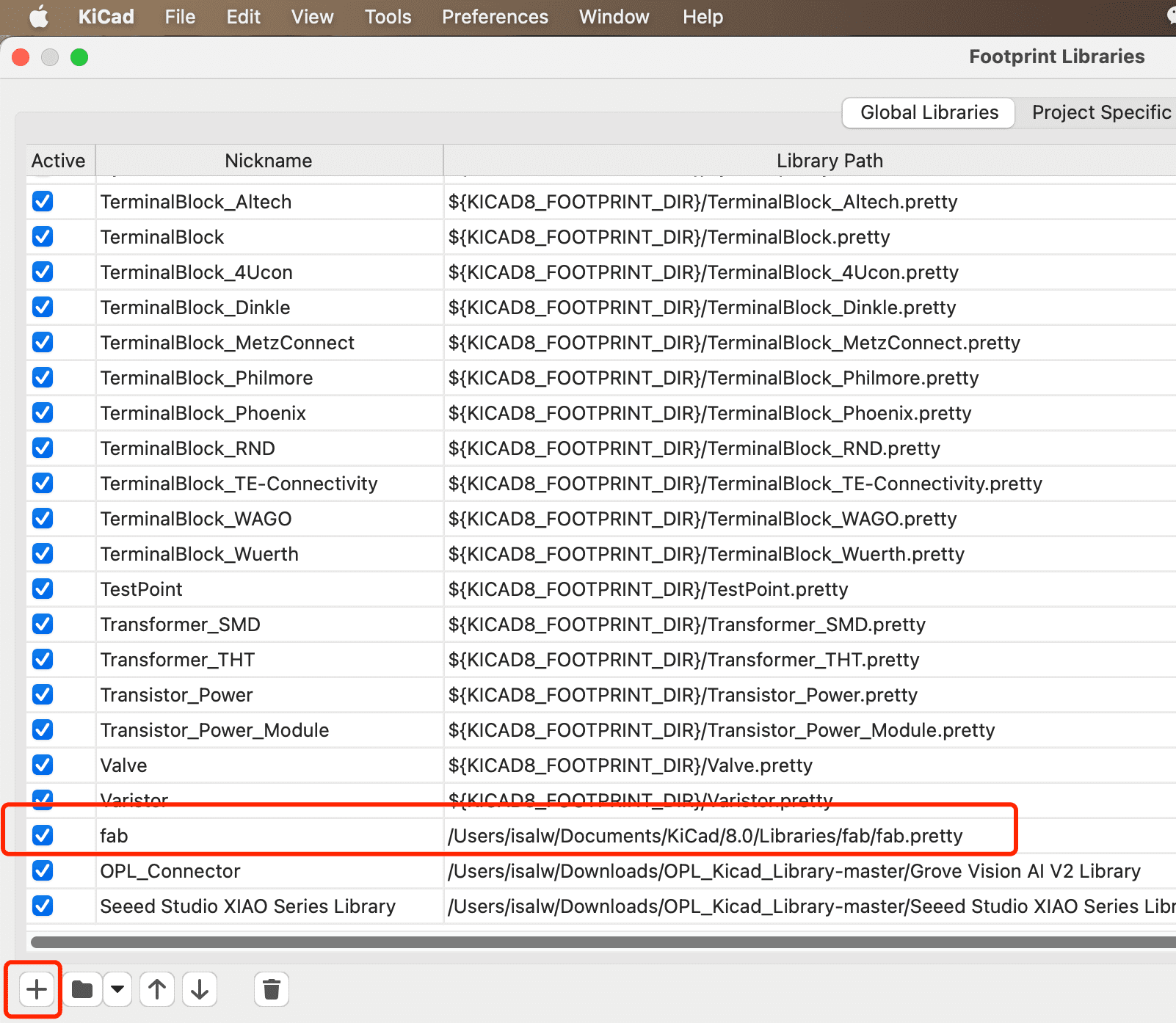
Before adding electronic components to your schematic, the libraries of the components from fabacademy needs to be installed first. You can use following link to download the libaries and follow the steps to add the libaries into your KiCad.
Link to the fabacademy libraries!
Now we can begin the design the schematic: First click "Add Symbol" button on the right side panel.
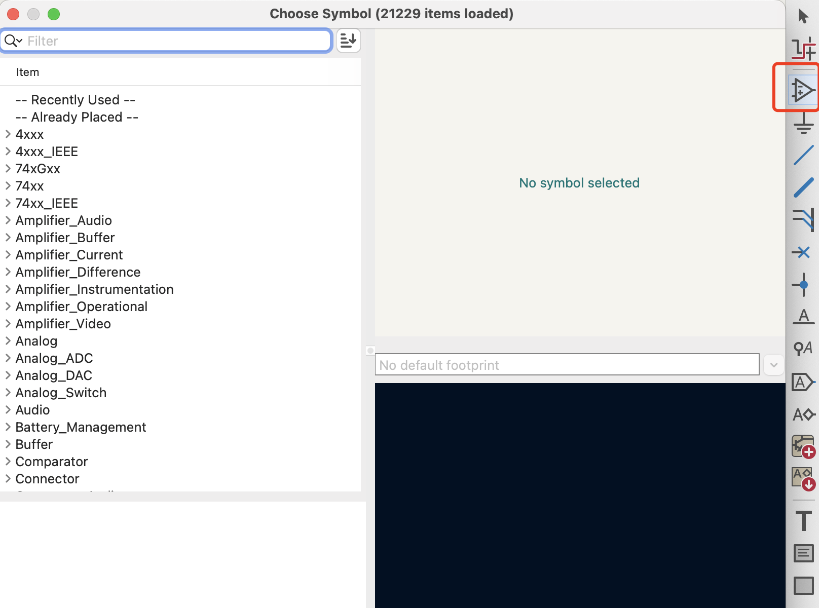
When selecting the compontent, you can search for the required components in the library, and once you click on the component's name, you can see both the schematic and PCB view of the componentsent needed in the libary and you can see both the schematic and PCB view of your components once click on the component's name.

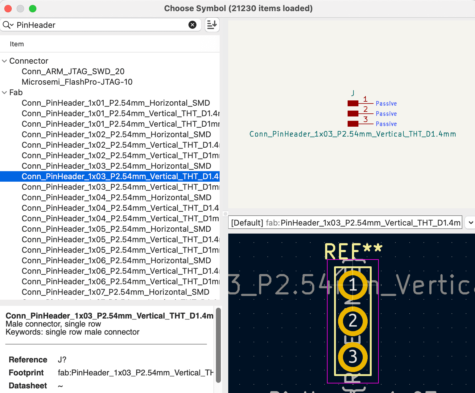
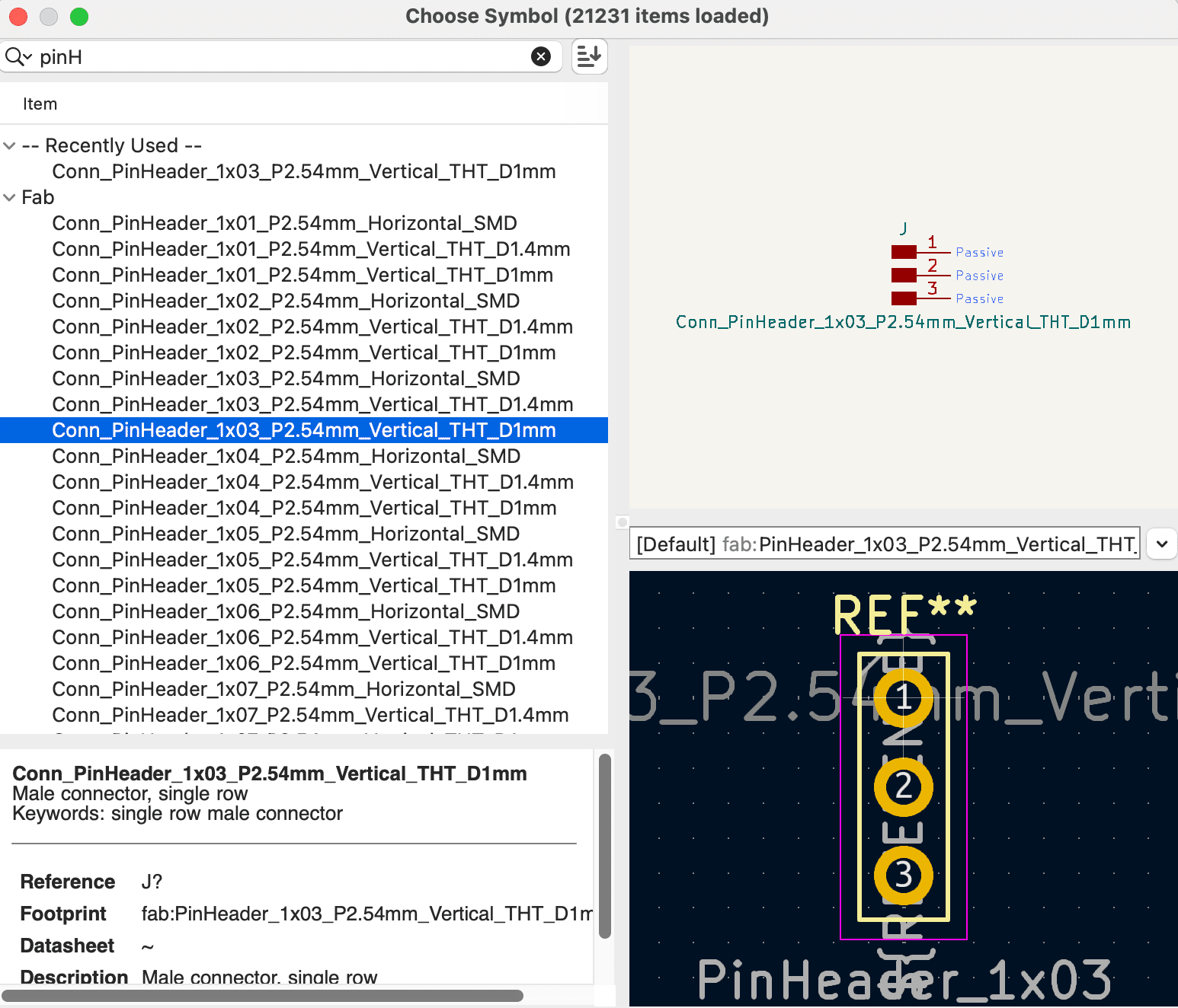
After the main component is placed on the schematic, we can continue to add more electronic components based on your design. Since my design will have the LED strip and a grove mp3 module potentially, so I need a group of three pin_header and a group of four pin_header. There are three different types of 1*3 pin_header, and you can tell the differences in the PCB view of the component: Take Conn_PinHeader_1x04_P2.54mm_Vertical_THT_D1mm as an example: - "Conn_PinHeader" indicates that this is a connector with a pin header. - "1x04" indicates that the pin header has 1 row with 4 pins. - "P2.54mm" means the pin pitch (spacing) is 2.54mm. - "Vertical" means the pin header is oriented vertically. - "THT" stands for Through-Hole Technology, meaning the pins are meant to be inserted through holes in a printed circuit board. - "D1mm" specifies that the diameter of the pins is 1mm.
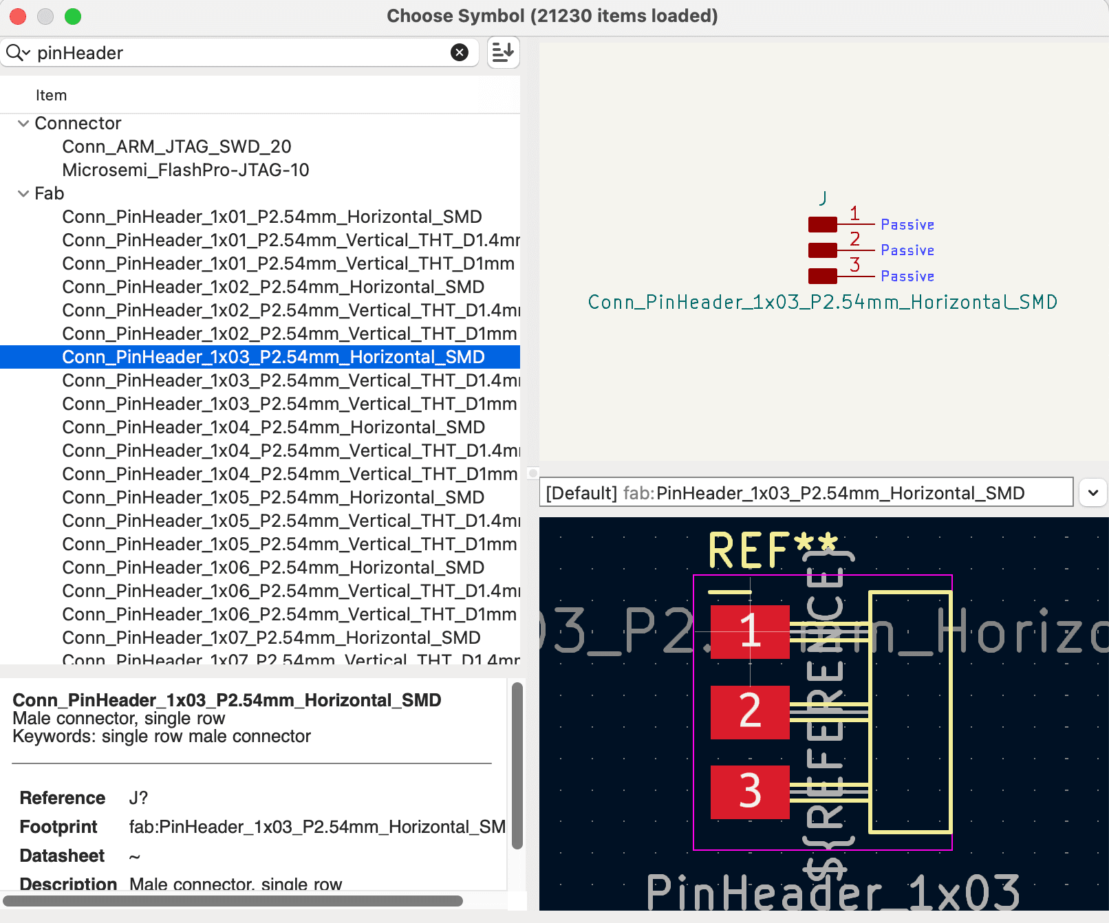
For my case, my choice is the Conn_PinHeader_1x03_P2.54mm_Horizontal_SMD
For the rest part, I just followed the pre-designed circuit design and drew lines connecting the components to the corresponding pins of the nRF52840.
Step 3 Update PCB from Schematic and Finish PCB Layout: First, click on component panel and choose the compontent you will use
When selecting the compontent, you can search for the required components in the library, and once you click on the component's name, you can see both the schematic and PCB view of the componentsent needed in the libary and you can see both the schematic and PCB view of your components once click on the component's name.
After the main component is placed on the schematic, we can continue to add more electronic components based on your design.
Since my design will have the LED strip and a grove mp3 module potentially, so I need a group of three pin_header and a group of four pin_header.
There are three different types of 1*3 pin_header, and you can tell the differences in the PCB view of the component:
Take Conn_PinHeader_1x04_P2.54mm_Vertical_THT_D1mm as an example:
- "Conn_PinHeader" indicates that this is a connector with a pin header.
- "1x04" indicates that the pin header has 1 row with 4 pins.
- "P2.54mm" means the pin pitch (spacing) is 2.54mm.
- "Vertical" means the pin header is oriented vertically.
- "THT" stands for Through-Hole Technology, meaning the pins are meant to be inserted through holes in a printed circuit board.
- "D1mm" specifies that the diameter of the pins is 1mm.
For my case, my choice is the Conn_PinHeader_1x03_P2.54mm_Horizontal_SMD
For the rest part, I just followed the pre-designed circuit design and drew lines connecting the components to the corresponding pins of the nRF52840.
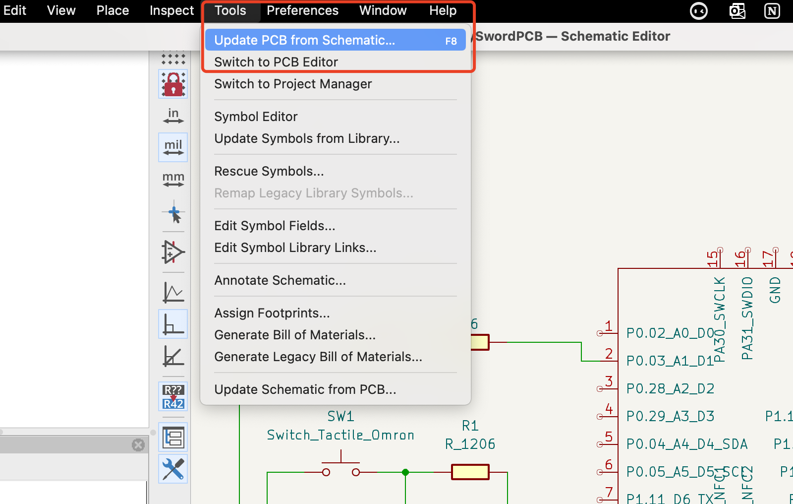
Step 4 Update Schematic to PCB
First go tools then click "update Schematic to PCB"
Then you will have the first view of your PCB
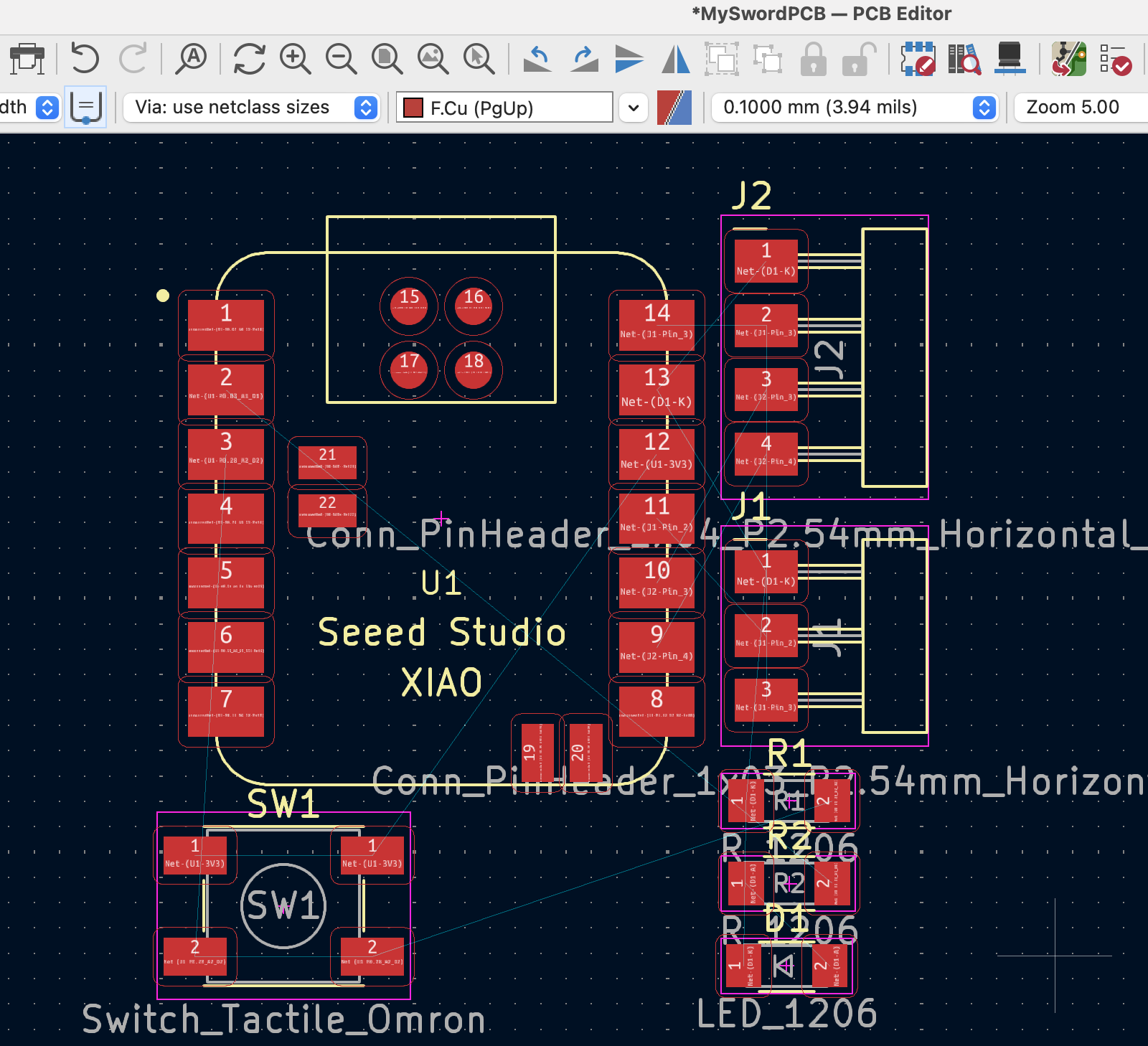
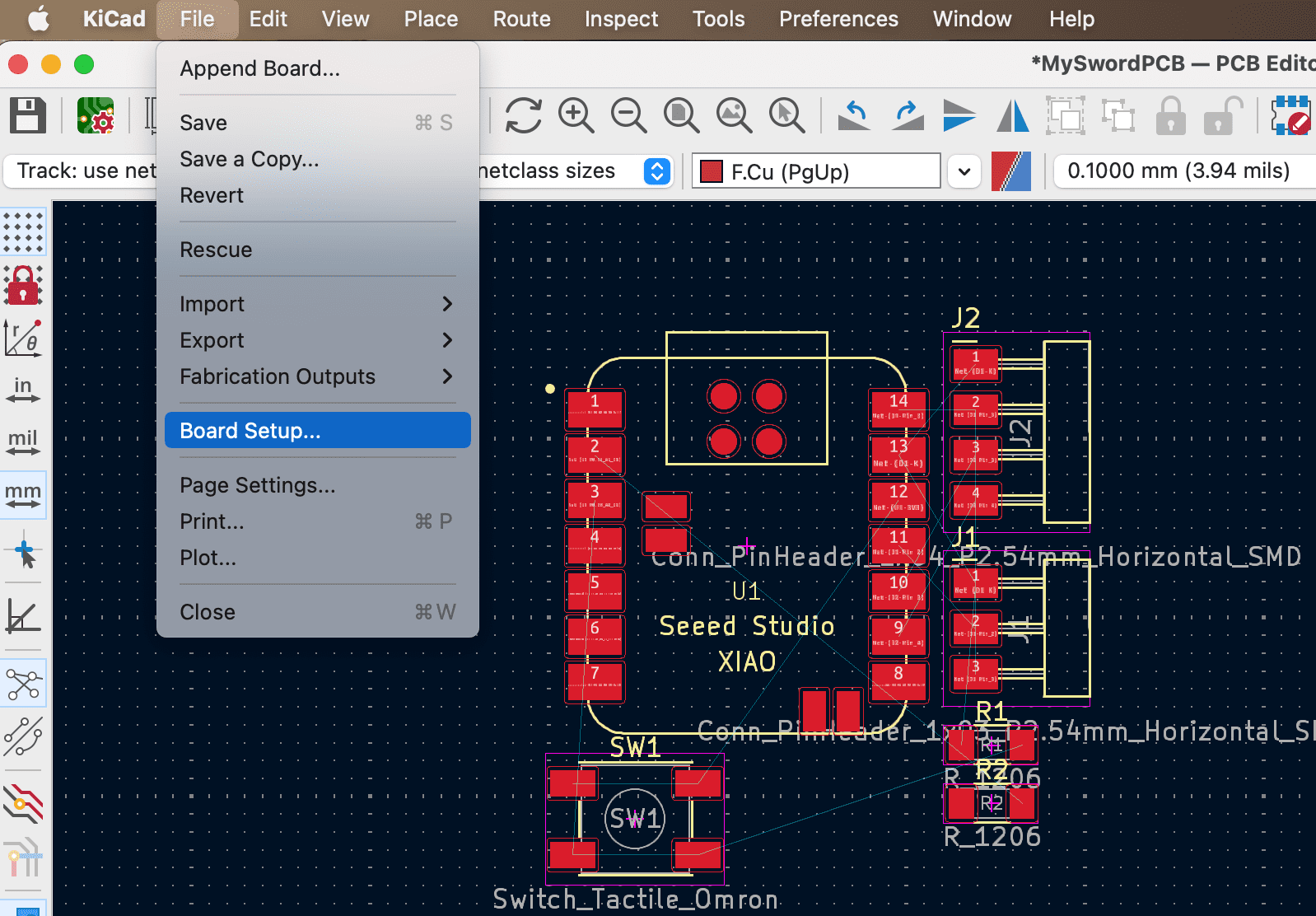
Secondly, set up the PCB rules for your PCB traces

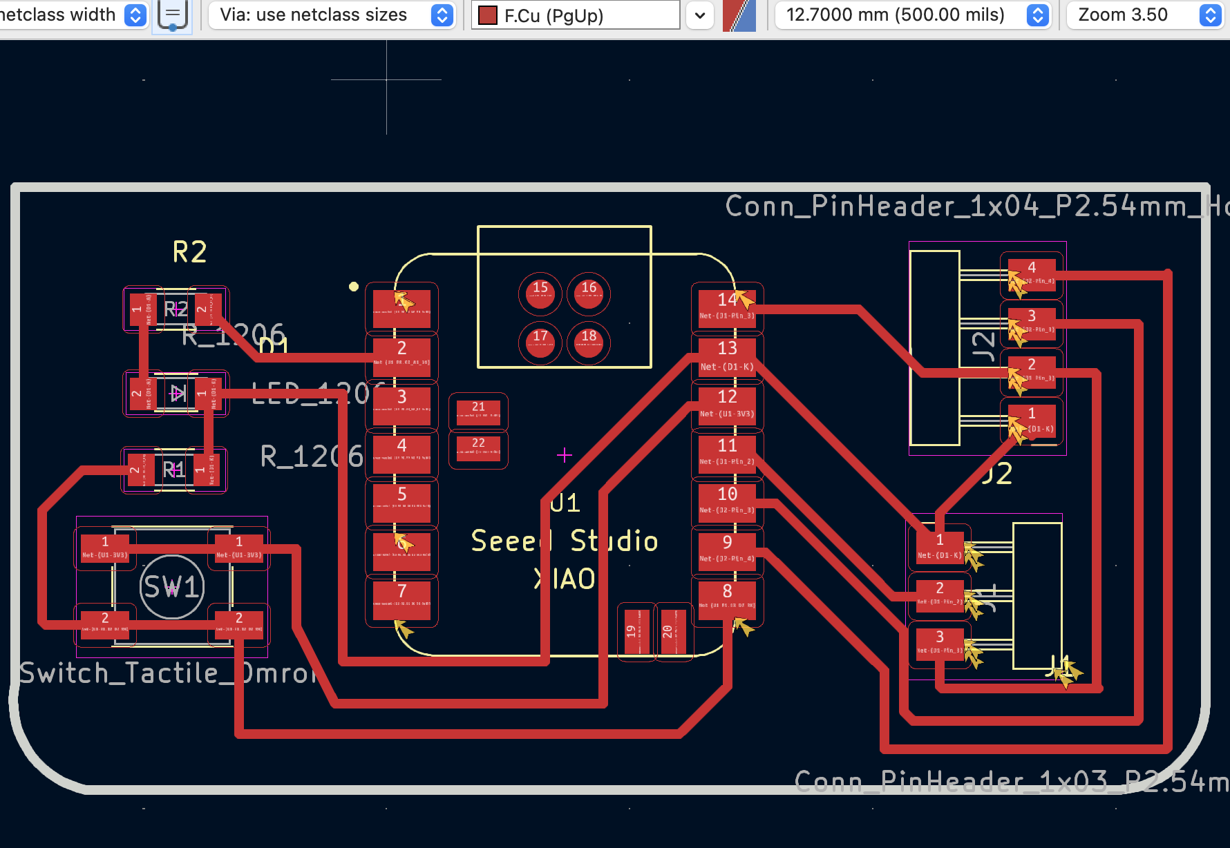
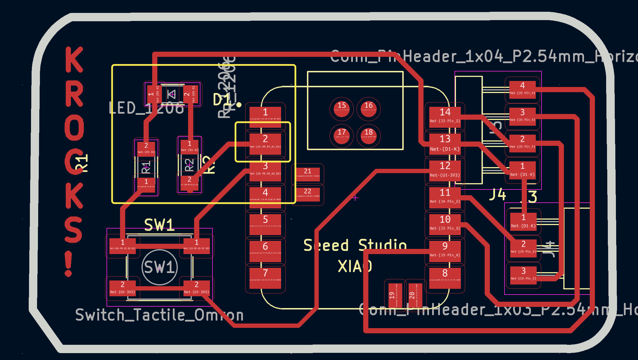
Now we can start to rearrange the compontents, the most important thing is to try to replace all the thin blue lines with PCB traces, and make sure there are no crossed points. If you see blue lines crossed as shown below, one option is to rotate the component positions to remove the crossing points.
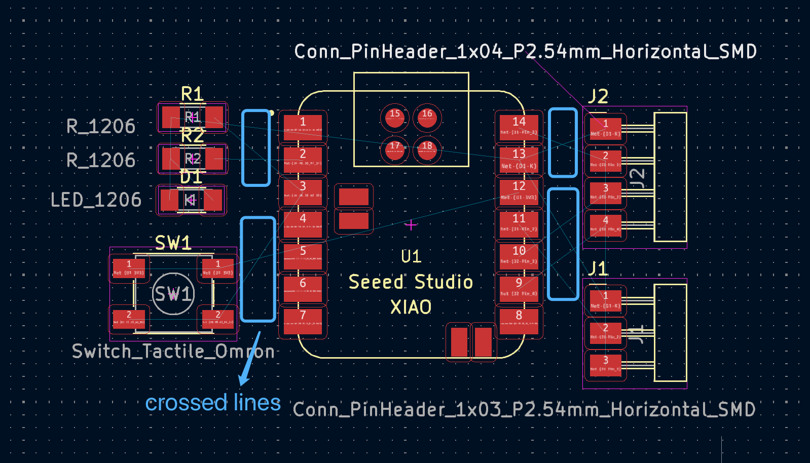

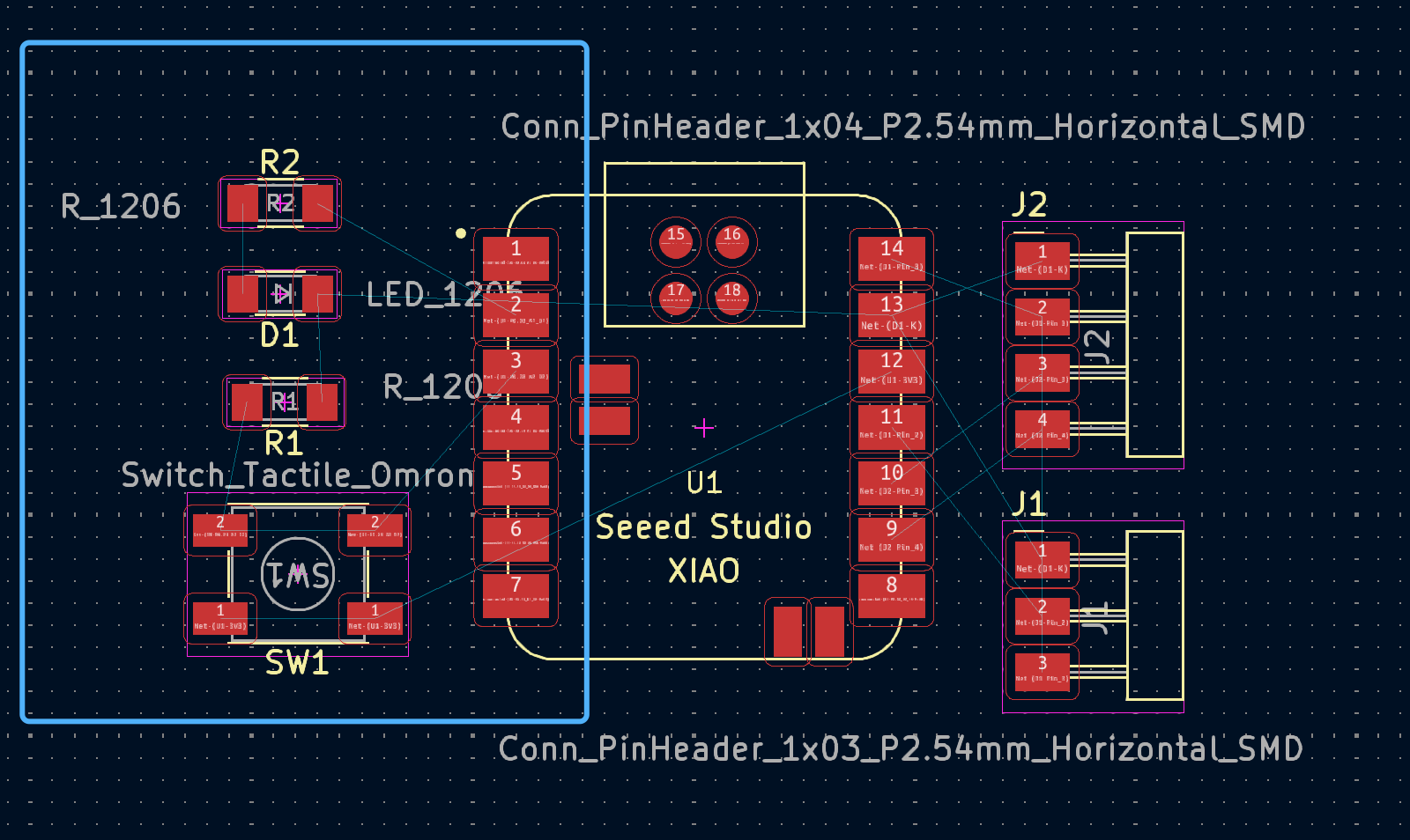
If you see blue lines crossed as shown in the 'crossed lines type2' example, the rotation method won't work. Instead, you can route one line inside and the other outside to avoid the crossing.
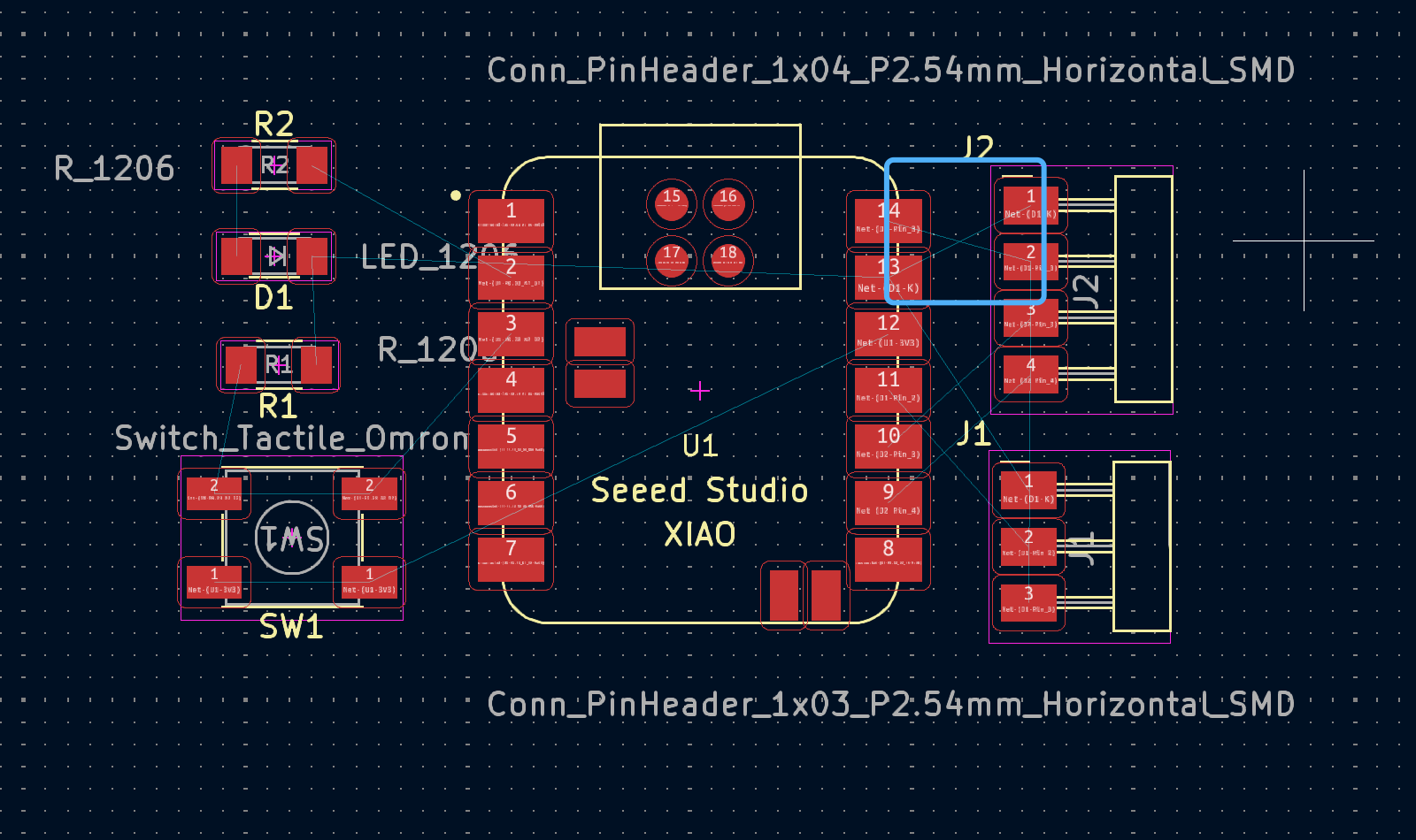
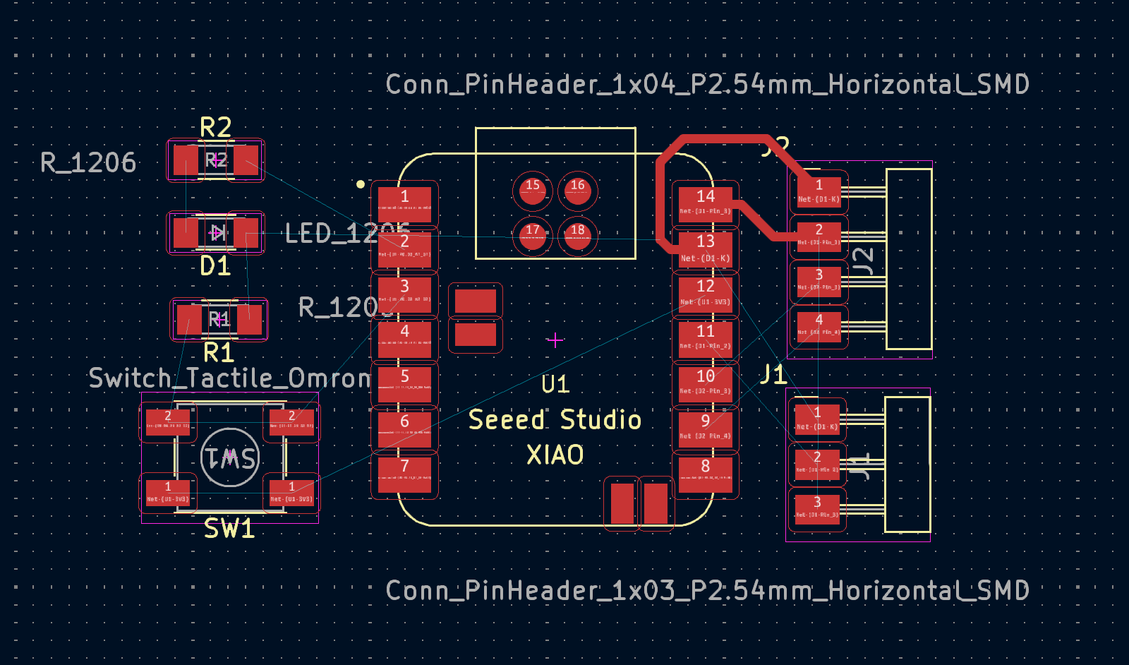
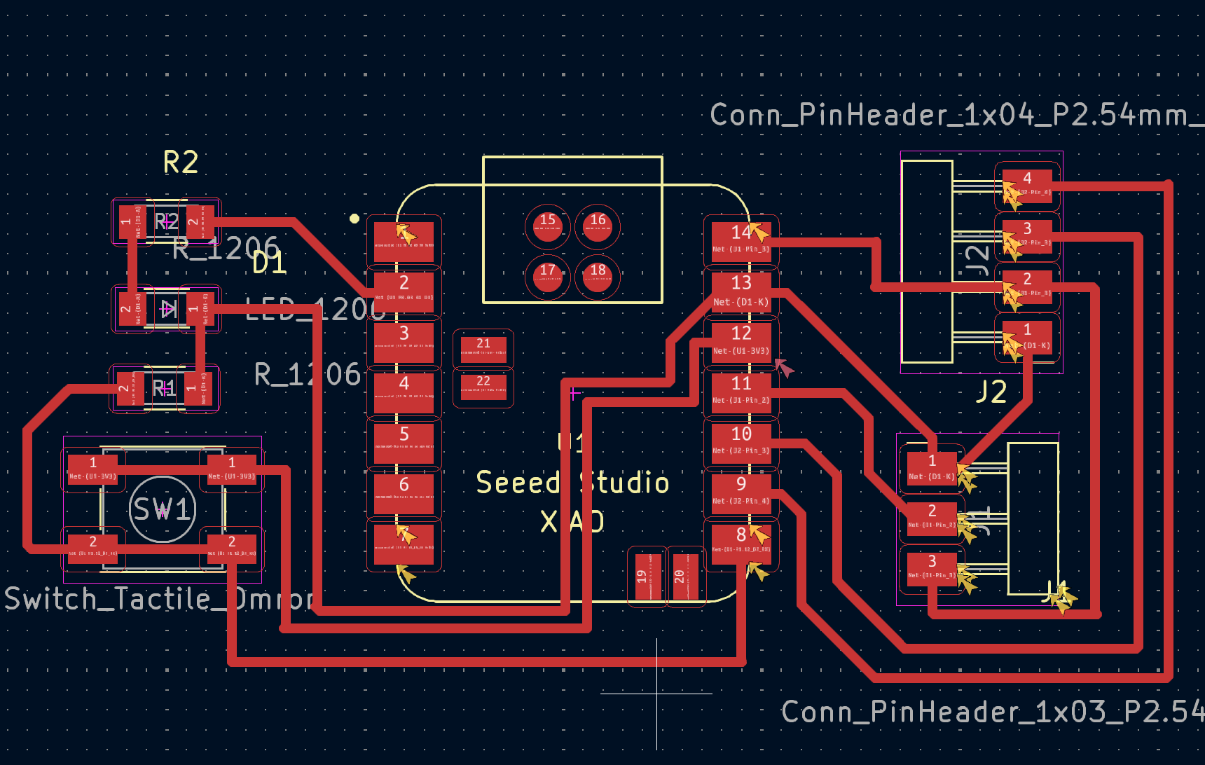
So basically, you will keep rotating the components and try all the angles to ensure there are no crossed lines. It is also recommended that you draw the circuit layout on paper first to get a better view. So after several rotations and changes to the positions of the components, the PCB is finally done without crossed lines. I even changed the connection pin of my switch from D2 to D8 to make the PCB layout easier.
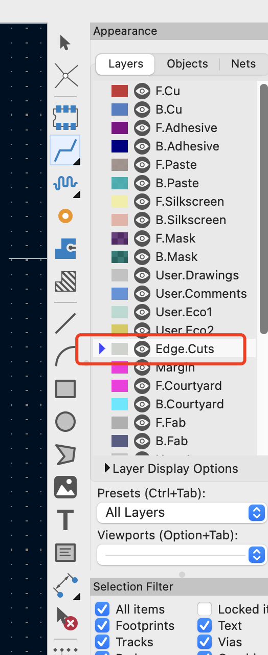
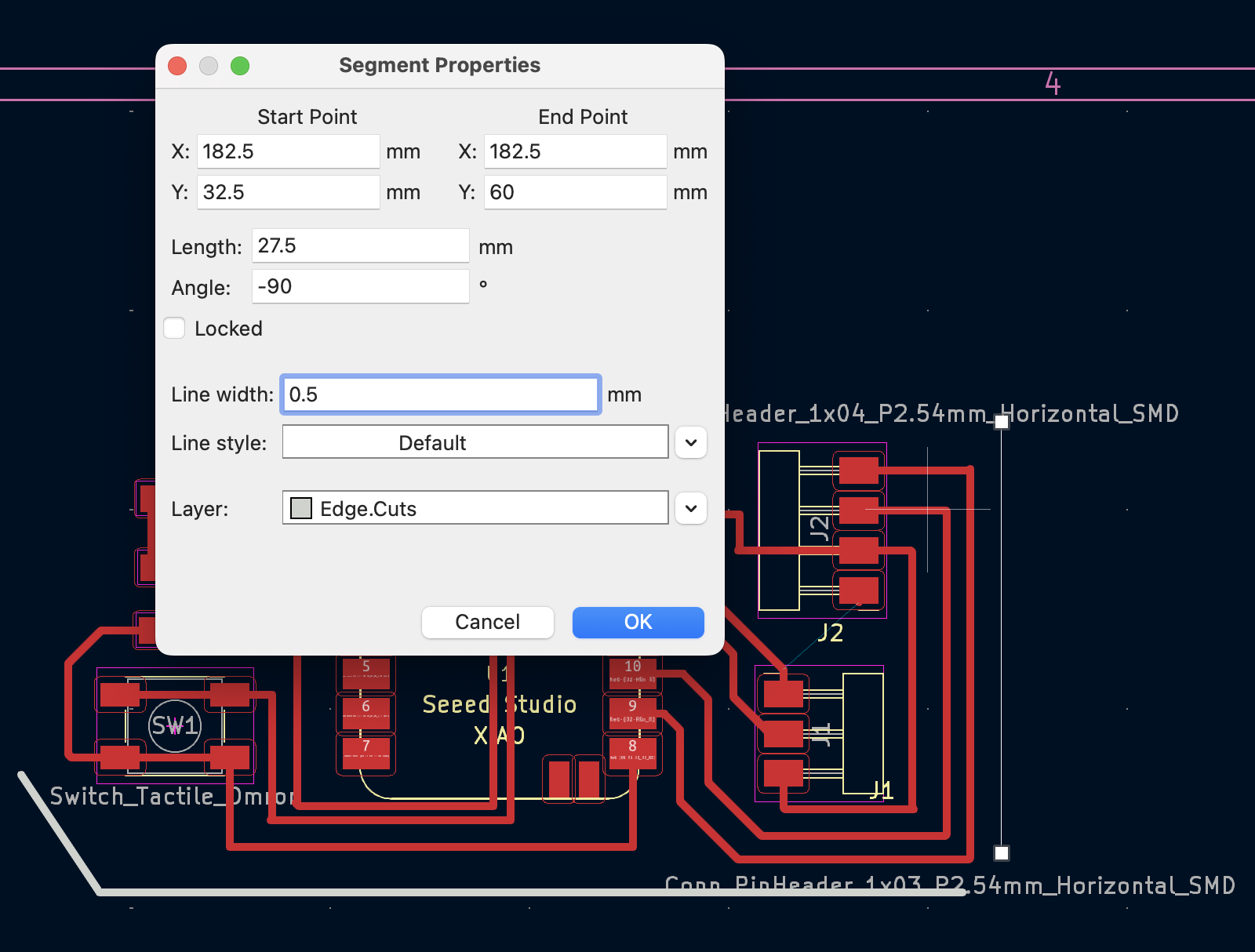
After this part is finished, the next step is the edge part of the PCB for the final outer layout of the whole PCB. For this step, switch to the edge layer first by selecting edge on the right side of the panel
 |
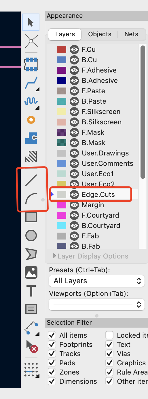 |
If the white line is too thin, double-click on the line and set the parameters about the thickness and position of the line. Additionally, the positions of the lines are a very important parameter, which can ensure the lines are properly connected to each other and save you trouble later.
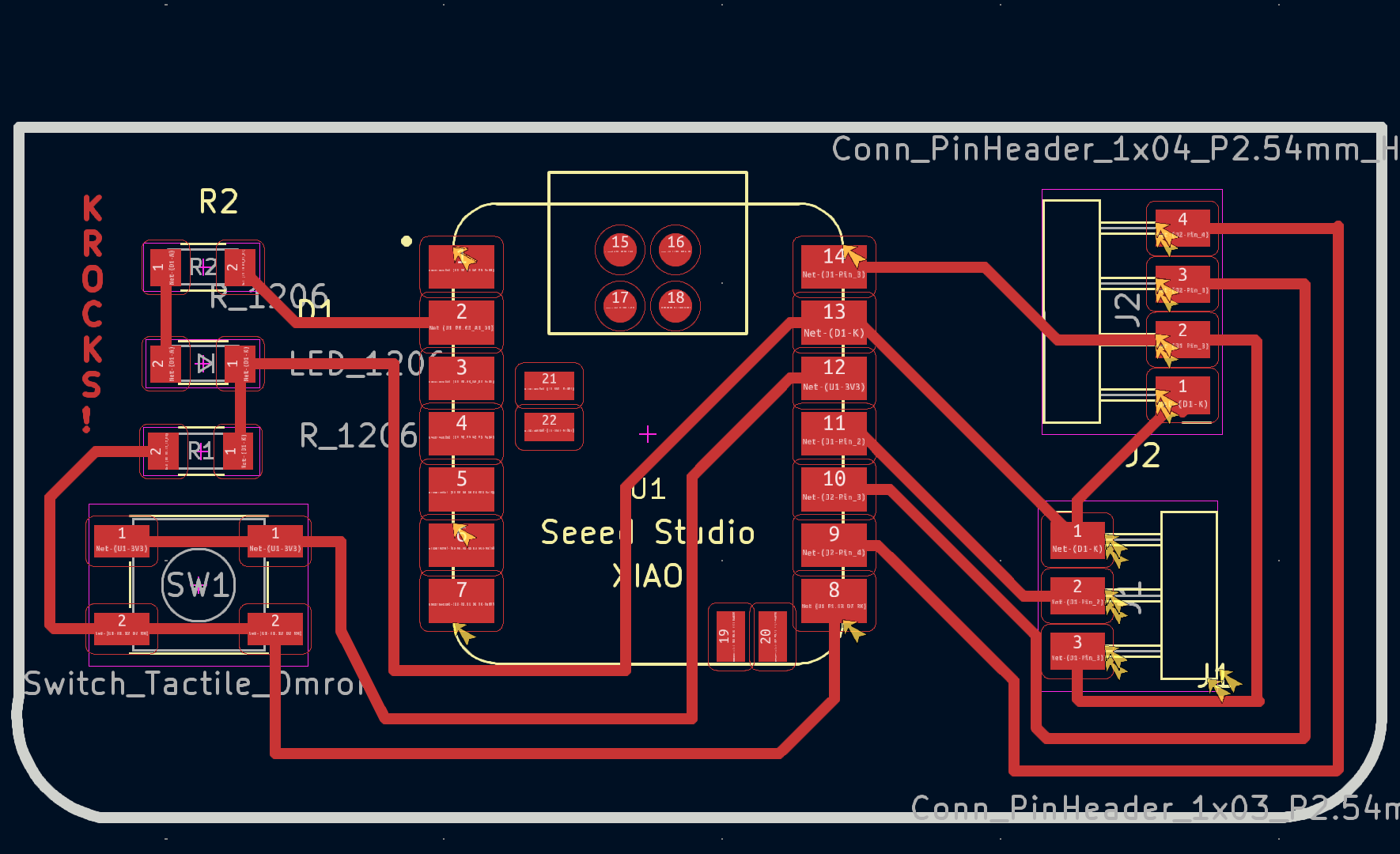
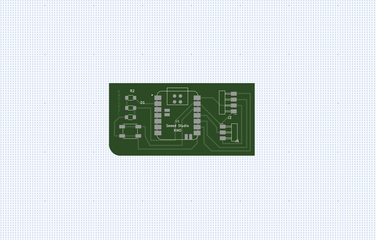
Finally, I finished my PCB as below:
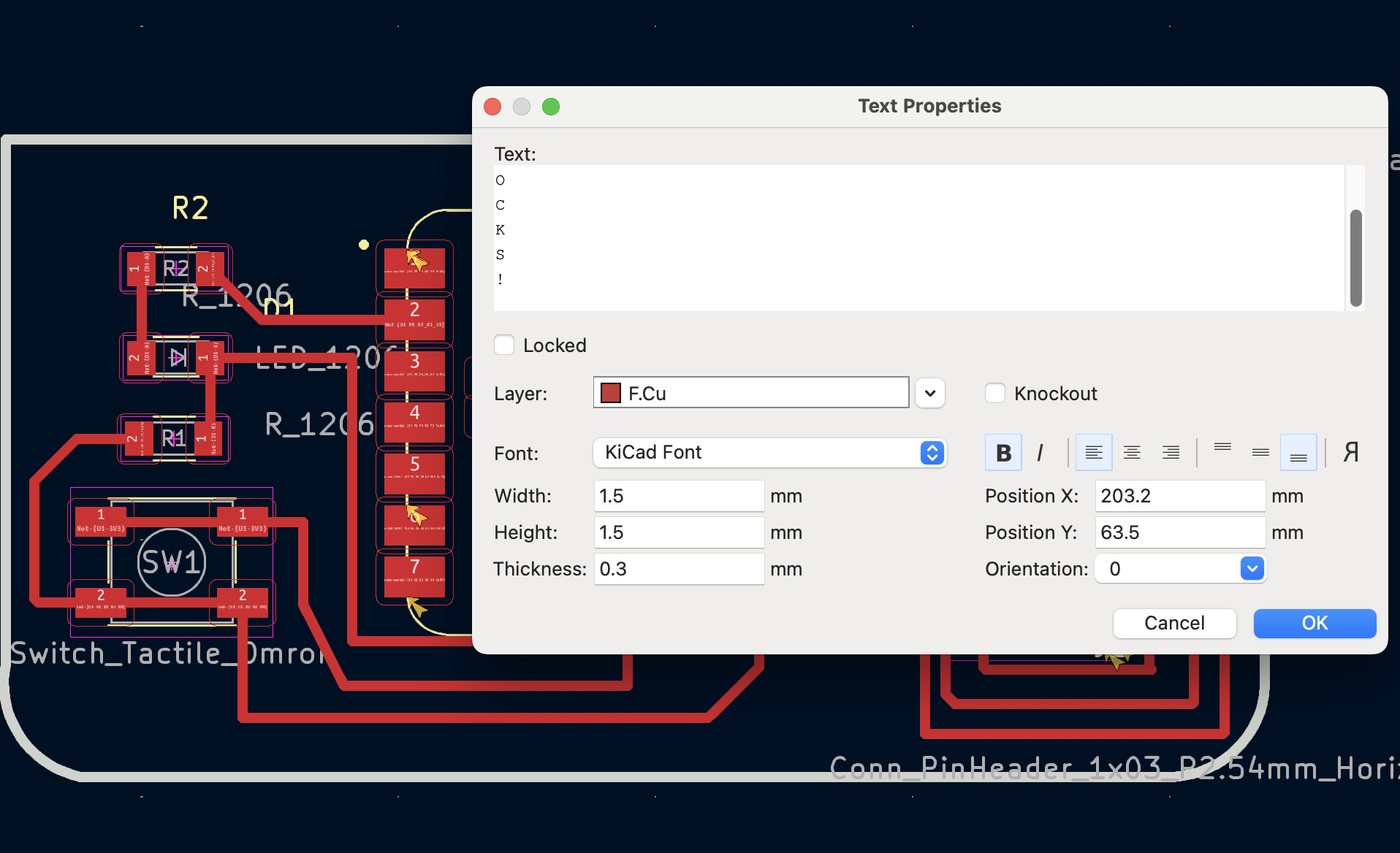
It is also fun to add some cute text on the board by using the text tool, but make sure it is placed on the F.Cu (Front Copper) layer.
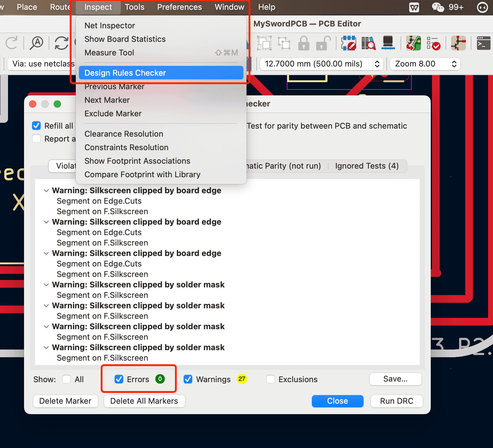
For the last step, run the inspection tool to fix all the errors until 0 errors are achieved.
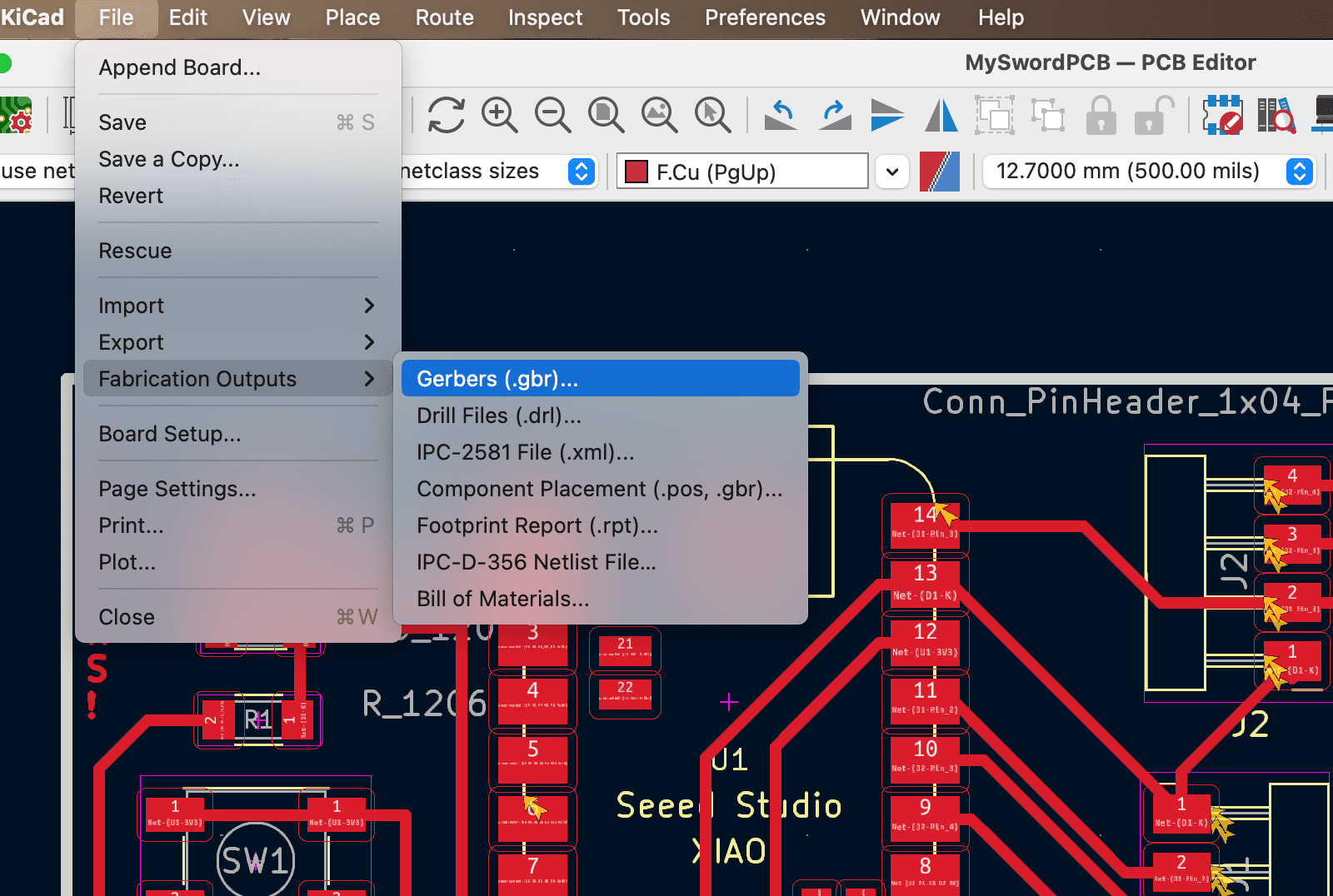
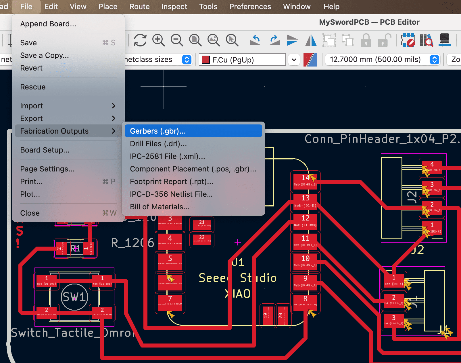
Step4 Generate Gerber files
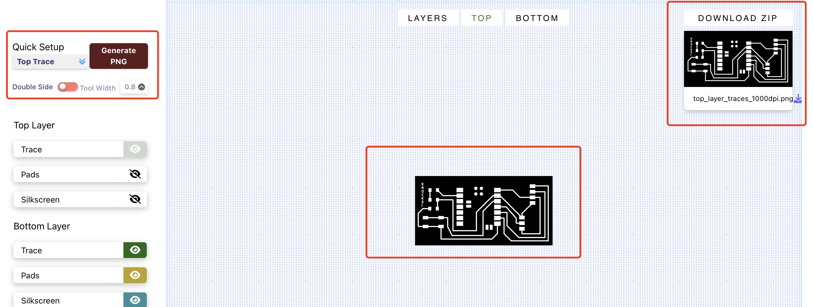
Step 5 Transfer Gerber file to PNG
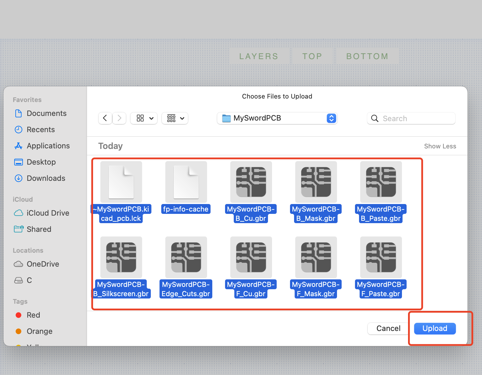
Select the topTrace and TopCut to generate corresponding png files.

Step 6 Generate the G-code Files using ModsCE
First, open the link as below:
It is needed to generate diffrent G-code files for trace cutting, outline cutting and drill.
For the trace file, the parameter needed to be set are as below
Always remember to set the dpi to 1000
For the v-bit, you can also change the parameter based on the real v-bit you have choosen instead of
using the default parameter to get a better PCB. The V-bit I have choosen 20 20
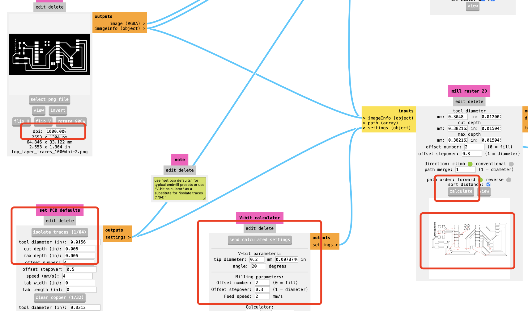
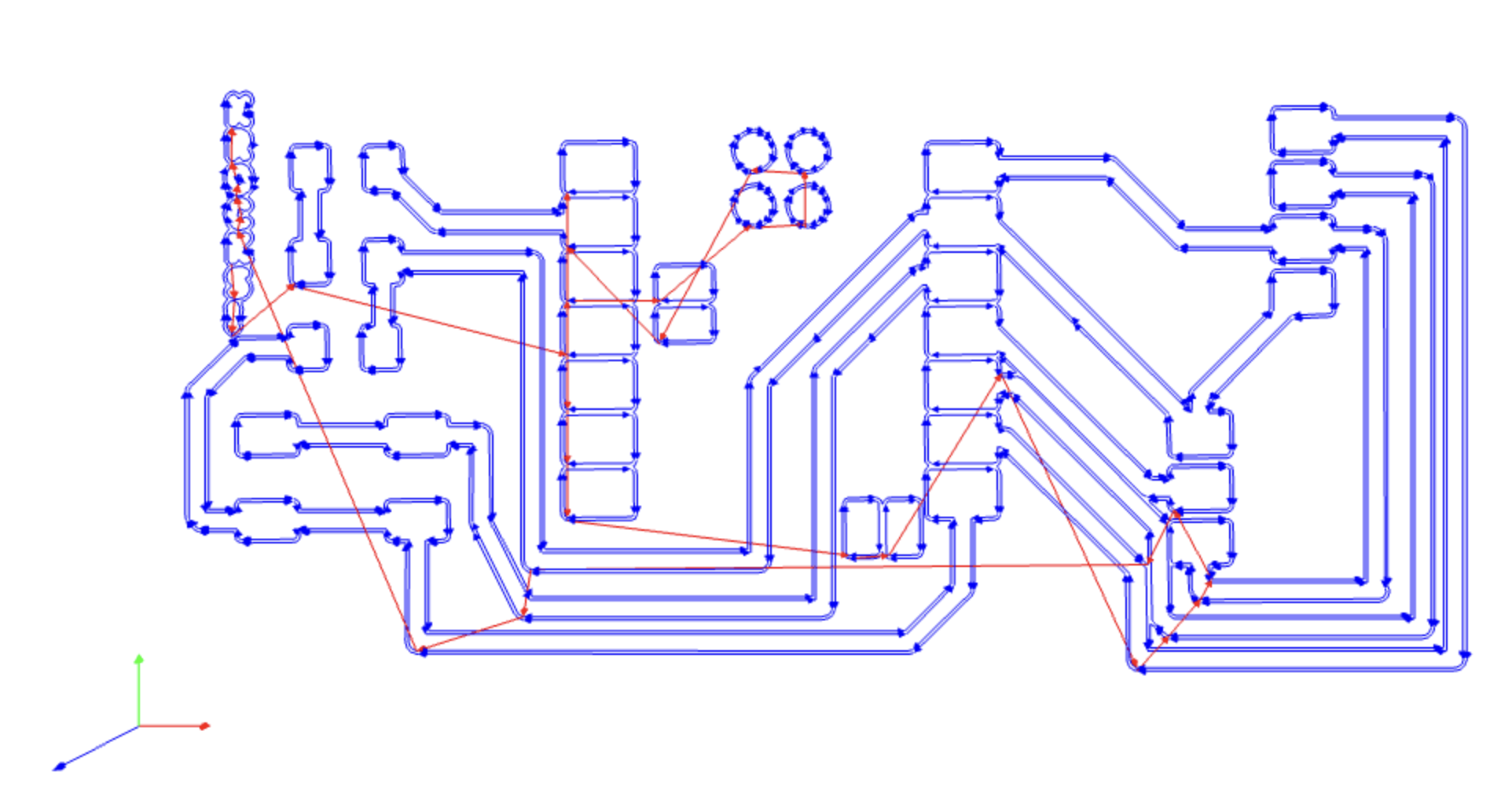
You can also preview the trace of cutting
For the outline file, the parameter needed to be set are as below:
Always remember to set the dpi to 1000
use the default parameter is fine.
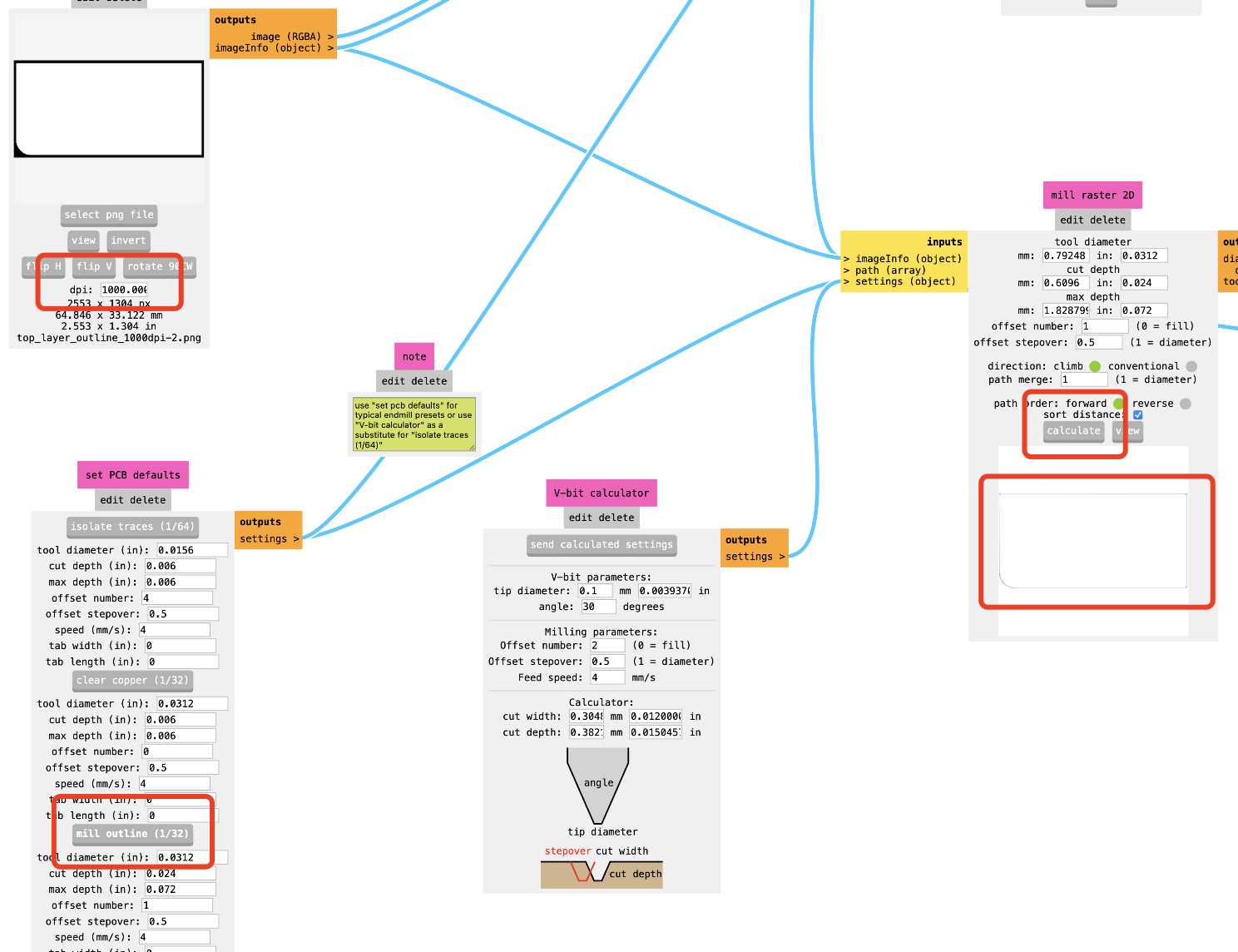
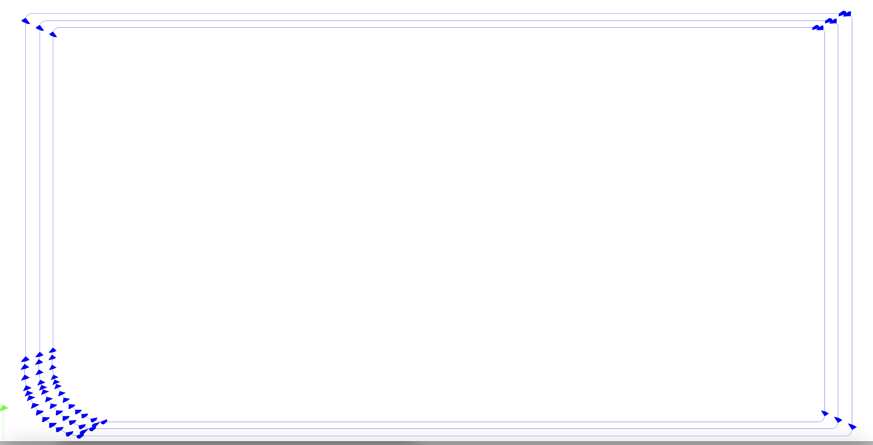
You can also preview the trace of cutting
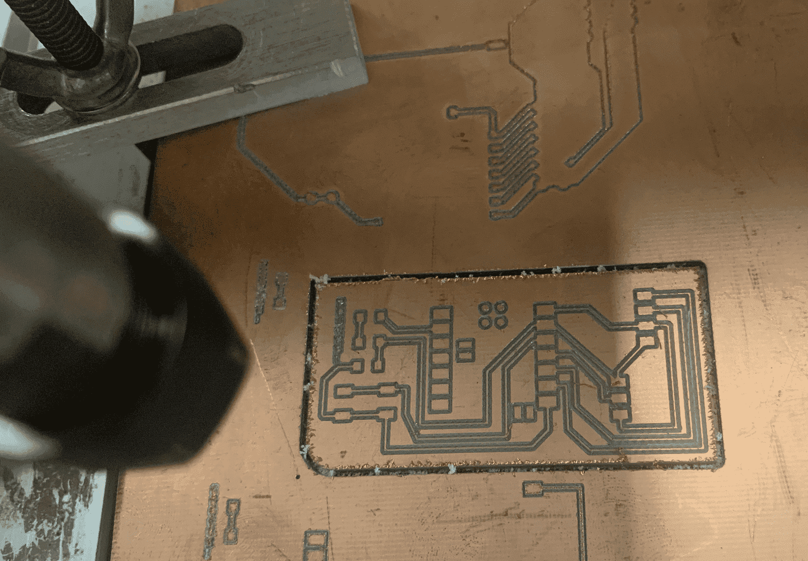
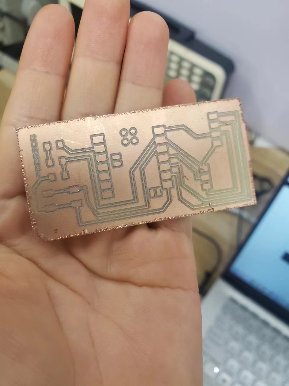
Step 7 Machine Milling
For this part, all needed is follow the same steps as week04 and use the machine to mill the PCB
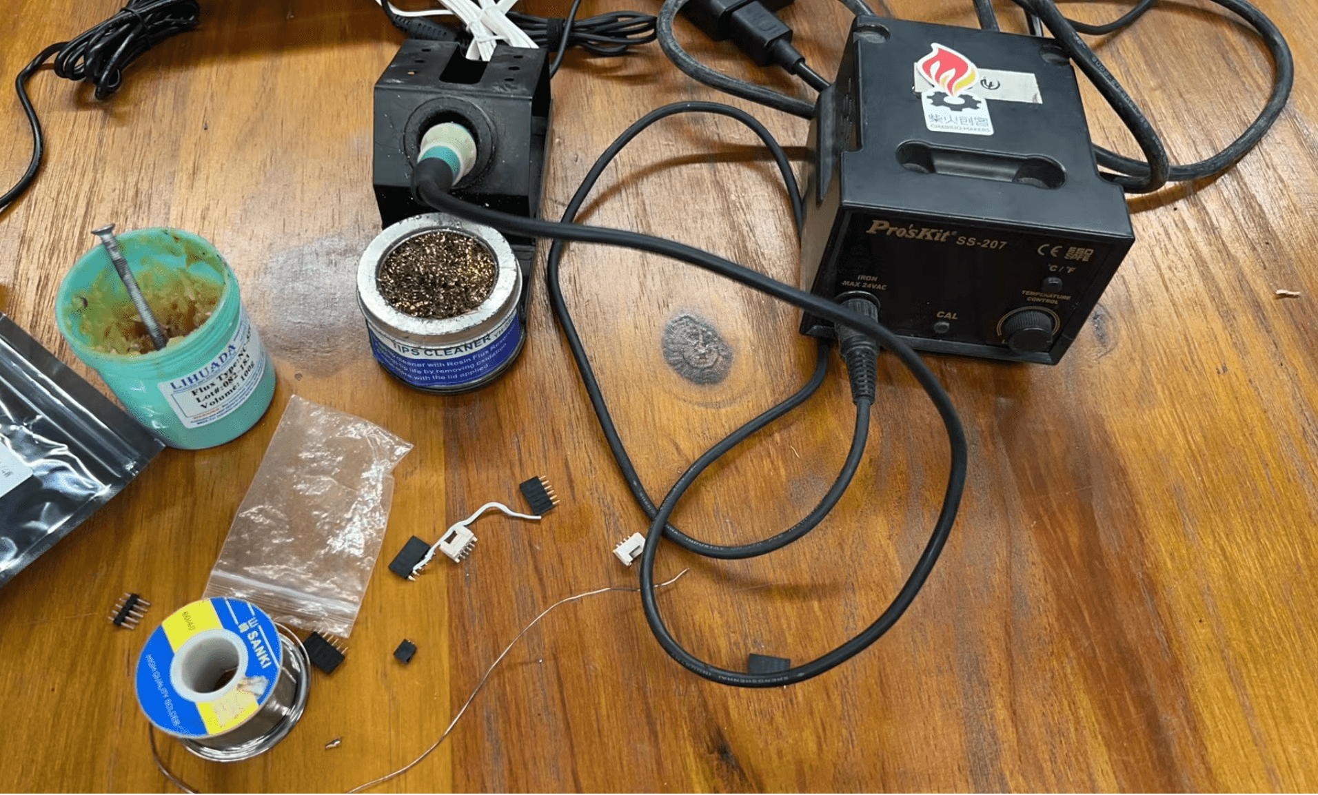
Step 8 Solder the Board
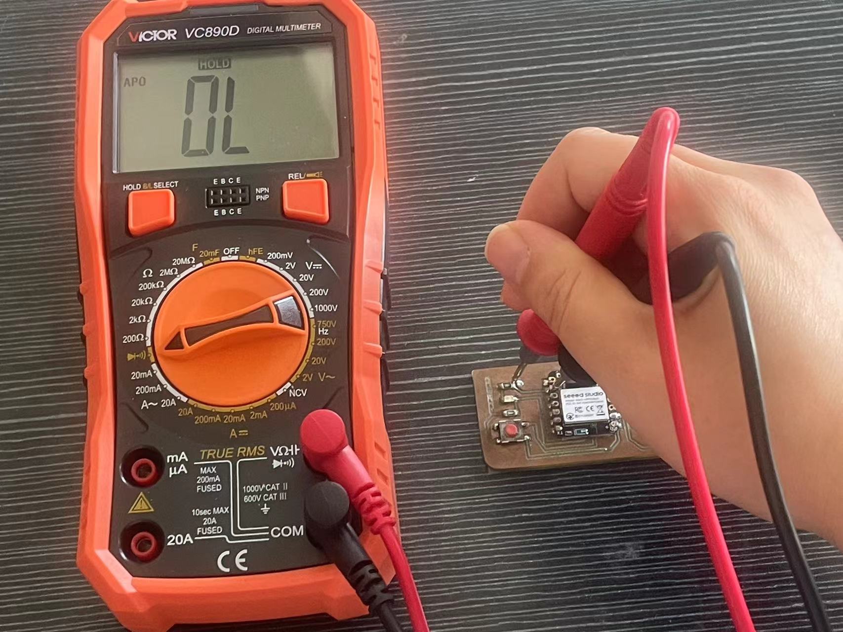
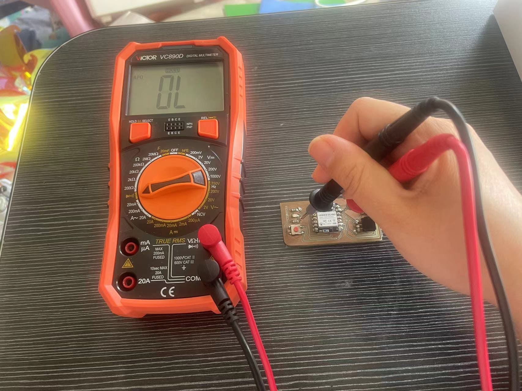
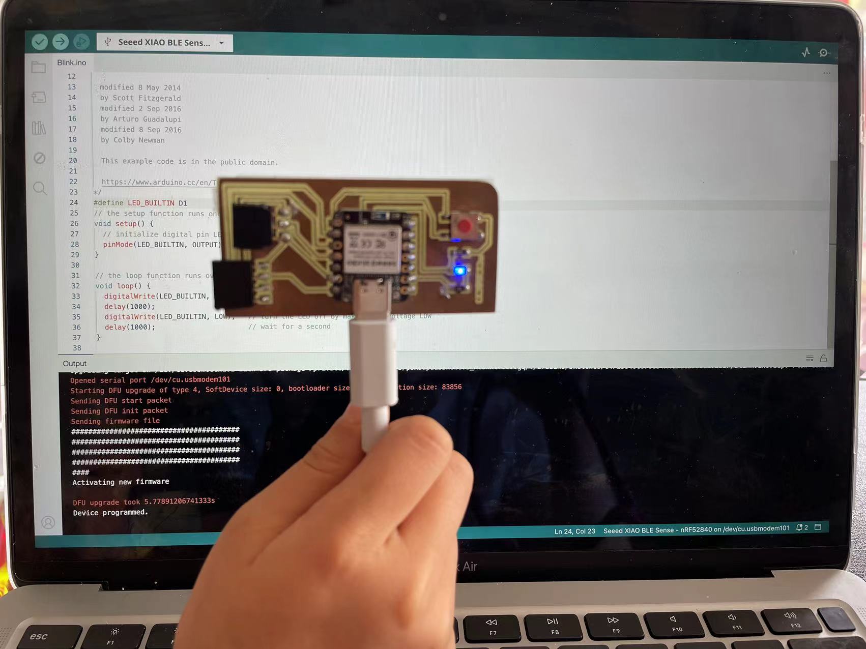
Step 9 Arduino Programming to blink the LED
Step1. Prepare nRF52840 sense board for Arduino Programming
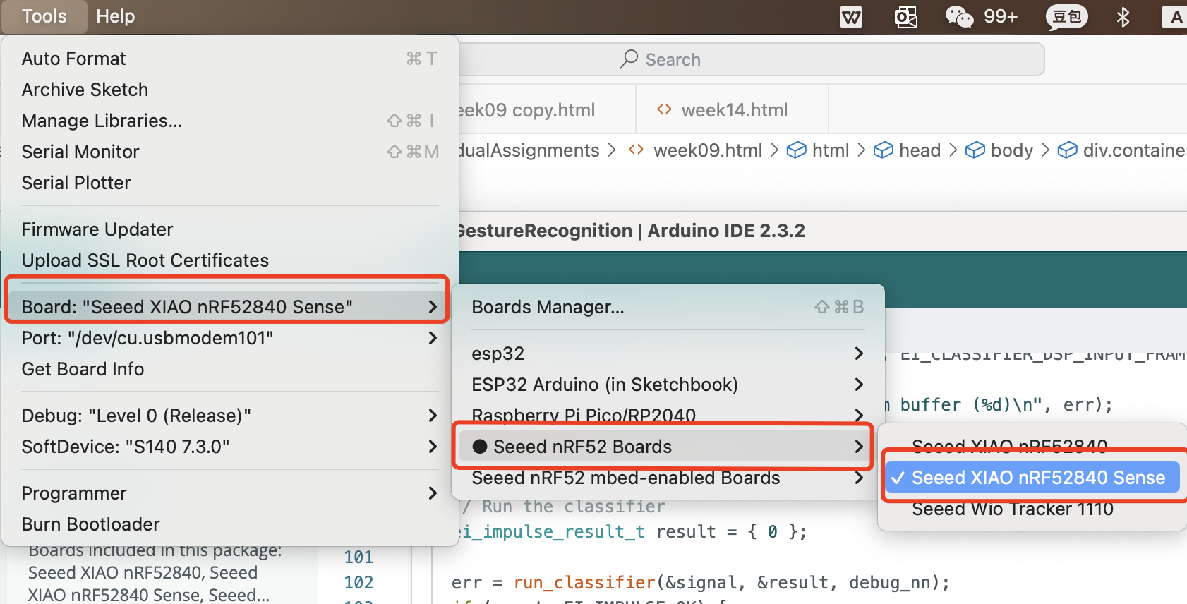
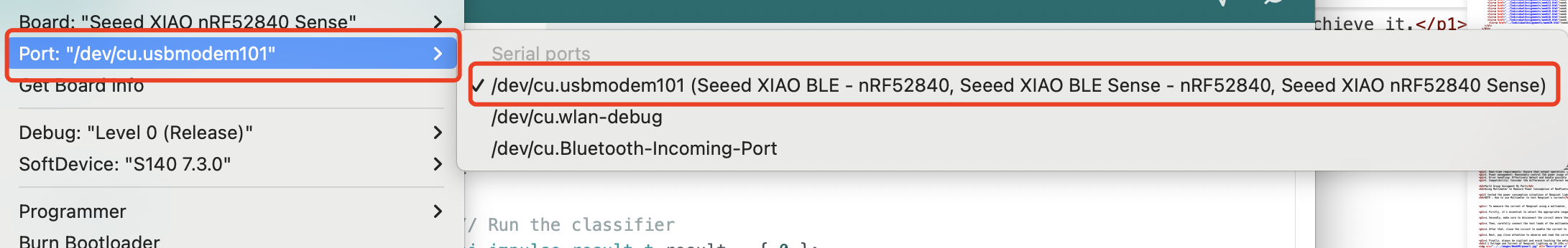
Step2. Arduino Programming
    #define LED_BUILTIN D1
    // the setup function runs once when you press reset or power the board
    void setup() {
      // initialize digital pin LED_BUILTIN as an output.
      pinMode(LED_BUILTIN, OUTPUT);
     }

    // the loop function runs over and over again forever
    void loop() {
      digitalWrite(LED_BUILTIN, HIGH);  // turn the LED on (HIGH is the voltage level)
      delay(1000);                      // wait for a second
      digitalWrite(LED_BUILTIN, LOW);   // turn the LED off by making the voltage LOW
      delay(1000);                      // wait for a second
    }