Weekly assignments
- week 1. Project Management
- week 2. Computer Aided Design
- week 3. Computer Controlled Cutting
- week 4. Electronics Production
- week 5. 3D Scanning and Printing
- week 6. Embeded Programming
- week 7. Computer Controlled Machining
- week 8. Electronics Design
- week 9. Output Devices
- week 10. Mechanical design & Machine Design
- week 11. Break & Midterm Review
- week 12. Input devices
- week 13. Moulding and Casting
- week 14. Networking and communications
- week 15. Interface and application programming
- week 16. Wildcard week
- week 17. System Integration
- week 18. Applications And implications
- week 19. Invention, intellectual property and income
Week4. Electronics Productiong
Group assignment:
Characterize the design rules for your in-house PCB production process
Individual assignment:
Make and test a microcontroller development boardThis week's assignment is mainly focused on PCB milling.
The key points for this week's assignments are:
- Mill the QT board provided by FabAcademy.
- Master the skills of milling a PCB using machining techniques.
- Test the final PCB.
Research
It is very important to watch Neil‘s video before the cutting and you will get exact information needed for this Assignment
PCB Design Softwares
1. Altium Designer:
Altium Designer is a comprehensive PCB design software widely used in the electronics industry.
It offers features like multi-board design, 3D PCB visualization, advanced routing capabilities, and integration with ECAD-MCAD collaboration.
Altium Designer is known for its powerful features and is often used for complex and high-density PCB designs.
2. KiCad:
KiCad is an open-source and cross-platform PCB design software.
It includes tools for schematic capture, PCB layout, 3D visualization, and design rule checking.
KiCad is a popular choice for hobbyists, small businesses, and educational institutions due to its free availability and growing community support.
3. Eagle (Autodesk Eagle):
Eagle (Autodesk Eagle) is a PCB design software known for its user-friendly interface and versatility.
It offers features like schematic capture, PCB layout, and integrated component libraries.
Autodesk Eagle has both free and paid versions, making it accessible to a wide range of users, from hobbyists to professional designers.
4. CircuitMaker:
CircuitMaker is a free, cloud-based PCB design software developed by Altium.
It provides a modern and intuitive user interface, allowing designers to create schematics, design PCBs, and collaborate with others in real-time.
CircuitMaker is a good choice for hobbyists, students, and small teams who want an accessible and feature-rich PCB design tool.
Useful links
PCB Production Procedures Software Part
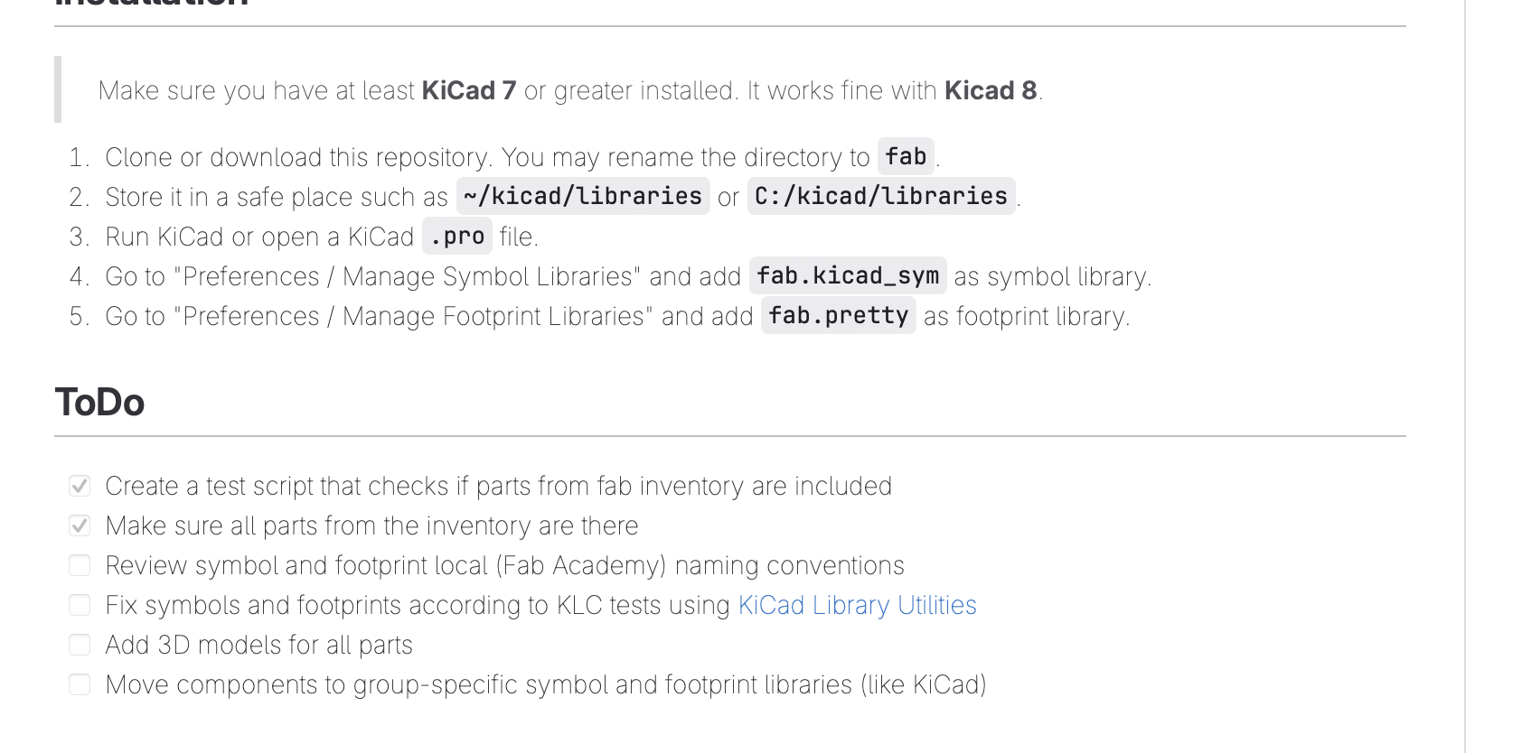
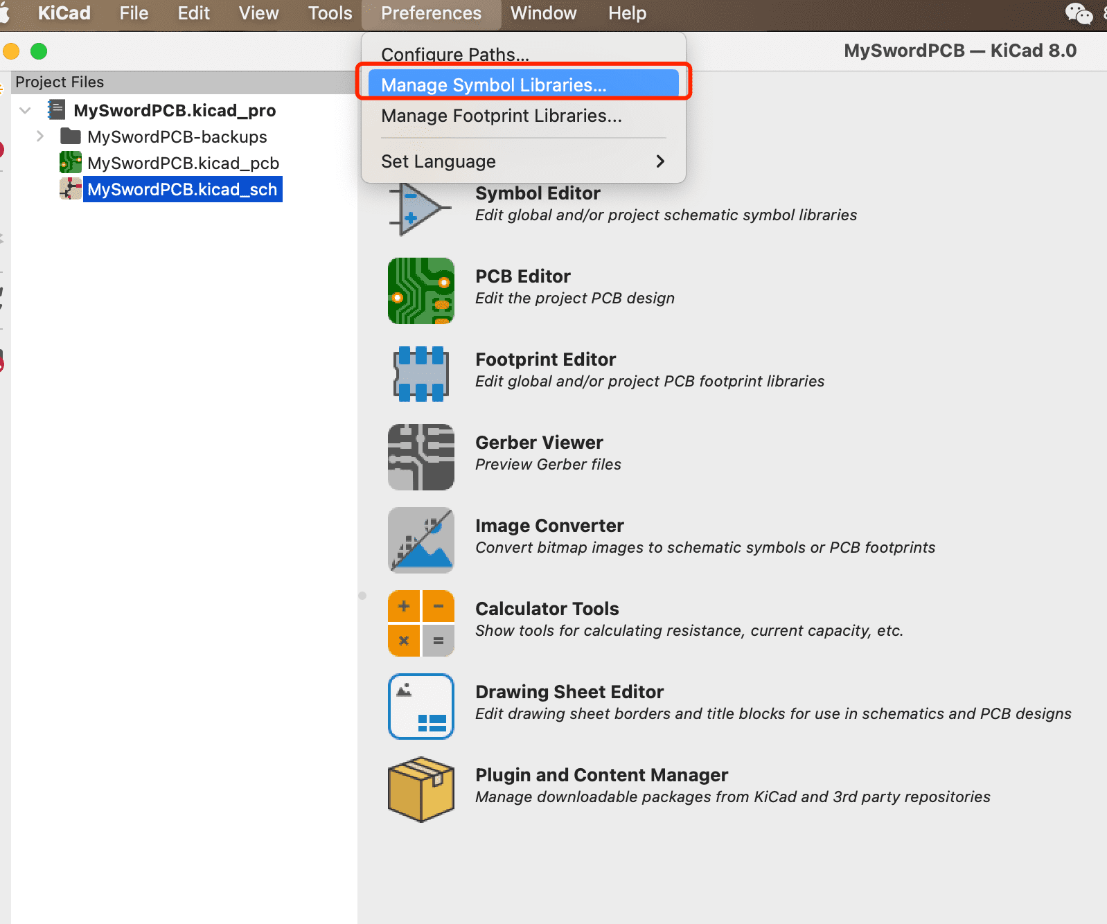
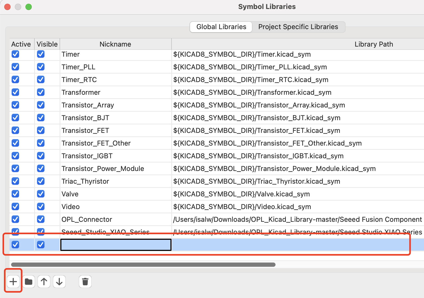
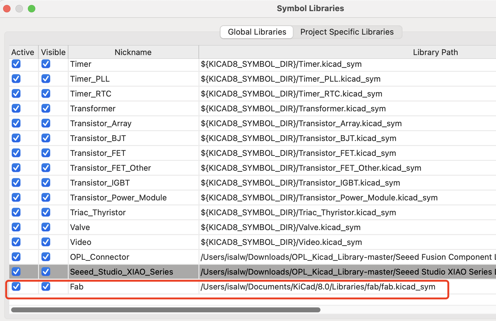
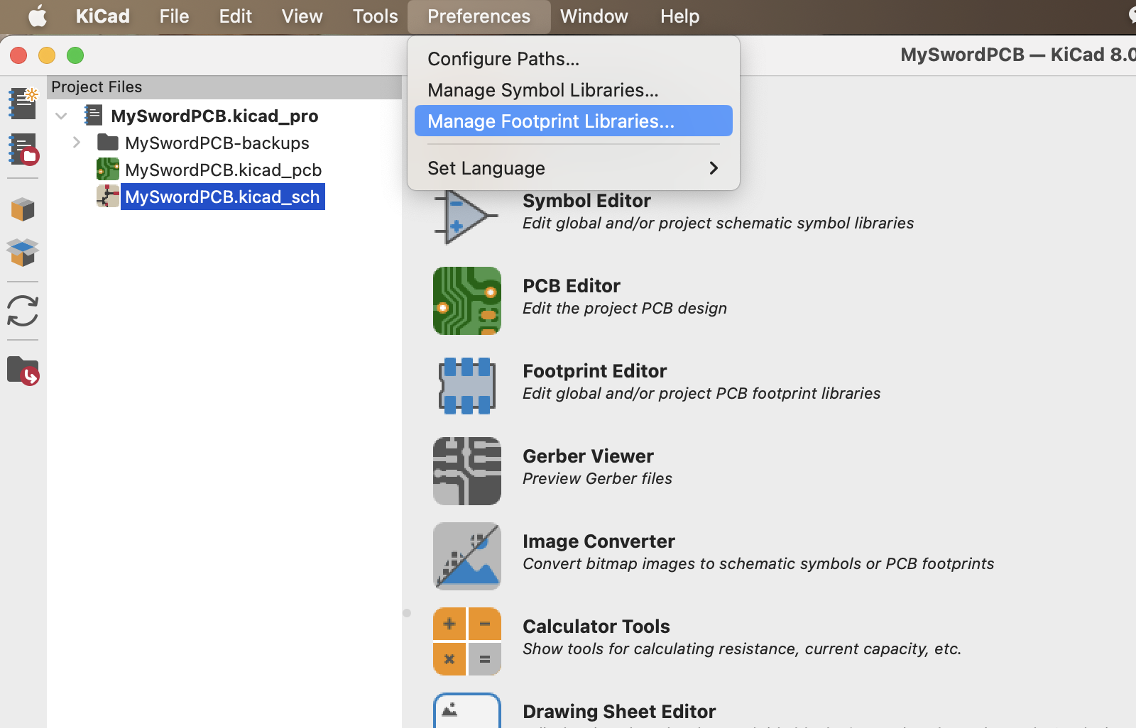
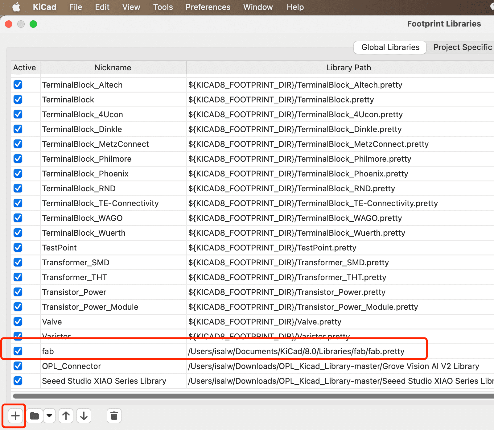
Step 1 Install the KiCad software and set up libaries
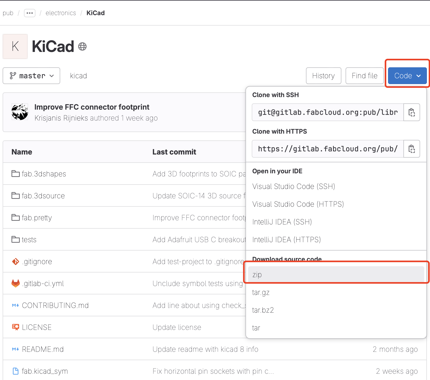
Libraries of the components from fabacademy needs to be installed first to start.
You can use following link to download the libaries and follow the steps to add the libaries into your KiCad.
Link to the fabacademy libraries!
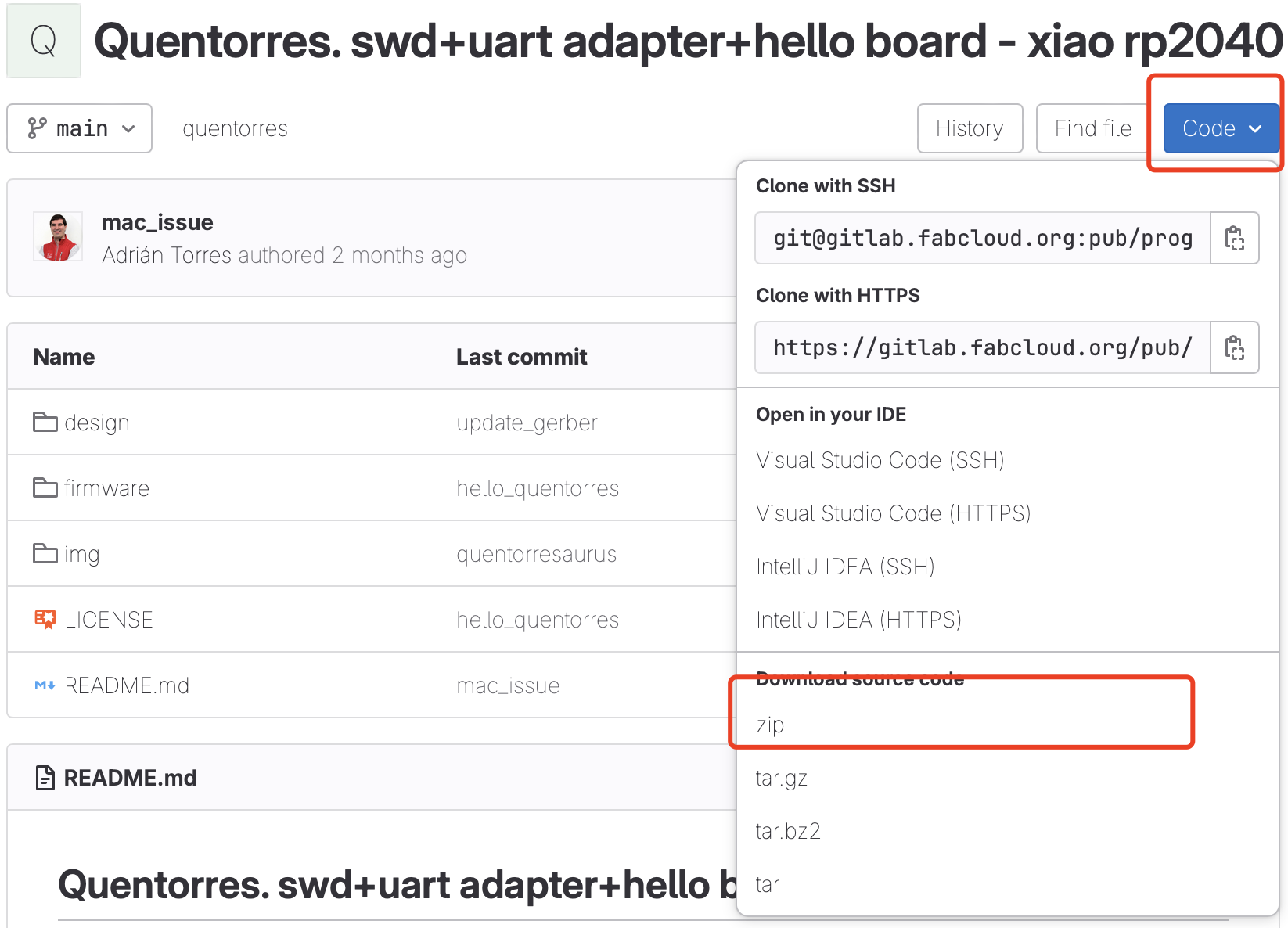
Step 2 Download the pre-designed PCB and schemetic files from FAB Academy Website!
The files should change every year, so make sure to download the file of your year.
Step 3 Open the PCB files using KiCad
The files should change every year, so make sure to download the file of your year.
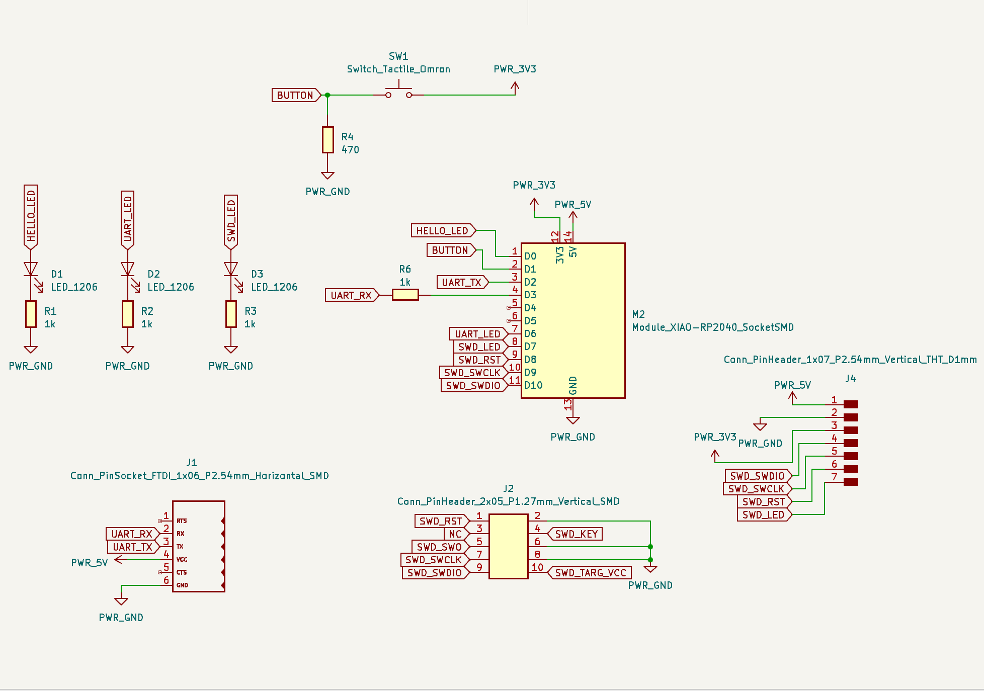
The schematic file is as below:
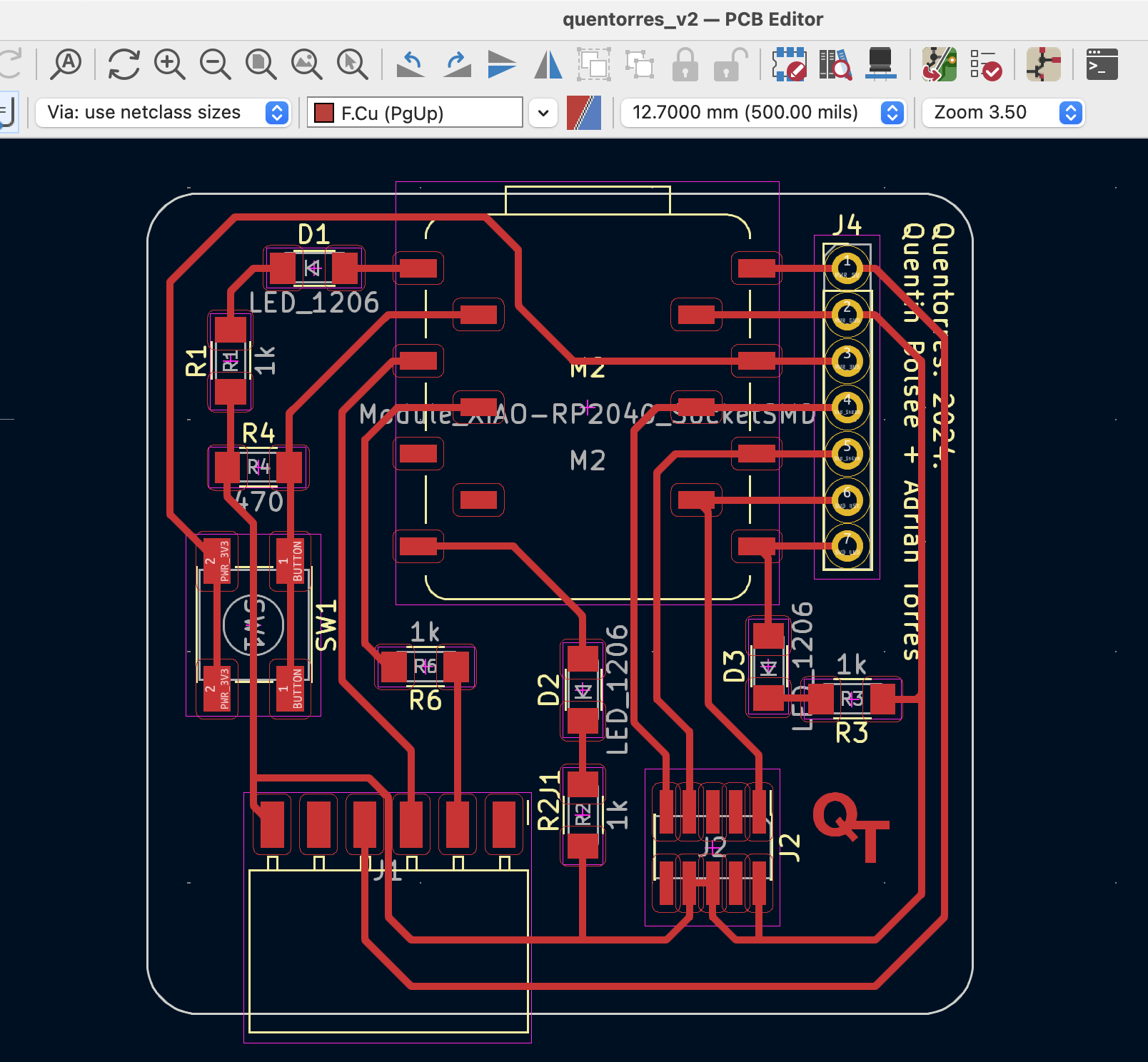
The PCB file is as below:
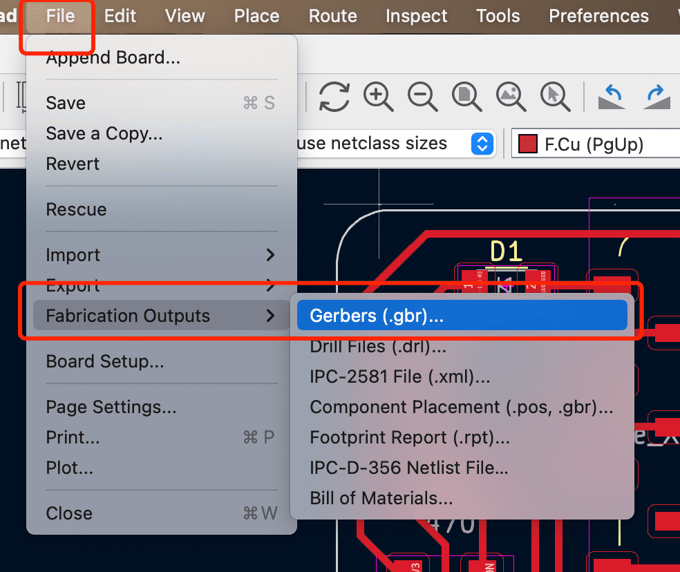
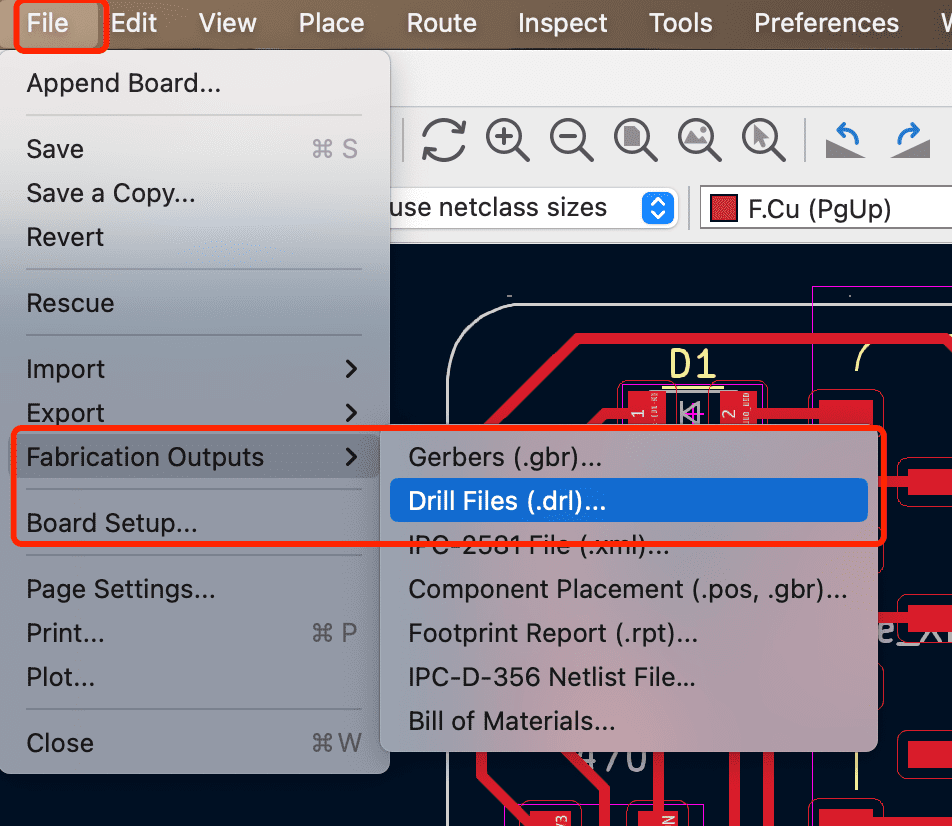
Step4 Generate Gerber files
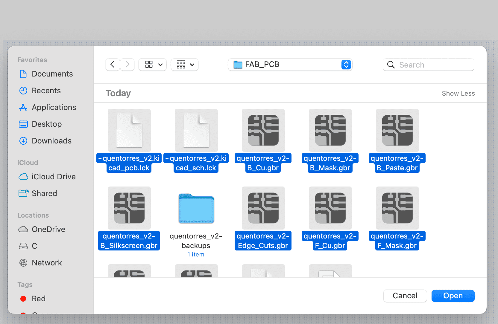
 <32> Step 5 Convert Gerber files to PNG images
First, open the link as below:
Choose all the gerber files in your folder
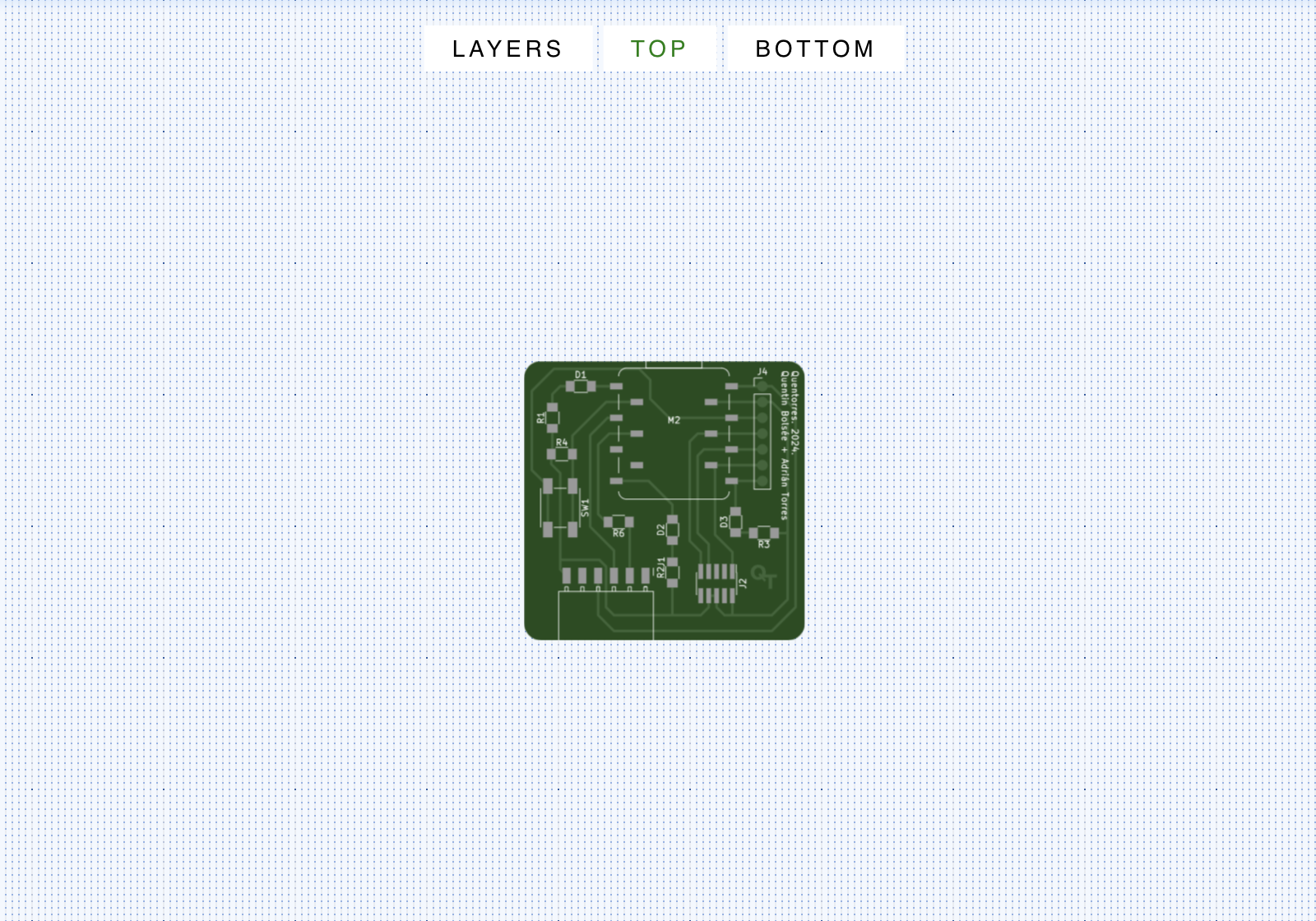
And you will have a basic view of your board image as below:
Step 6 Convert Gerber files to PNG images
First, open the link as below:
Choose all the gerber files in your folder
And you will have a basic view of your board as below:
Choose trace to create trace file
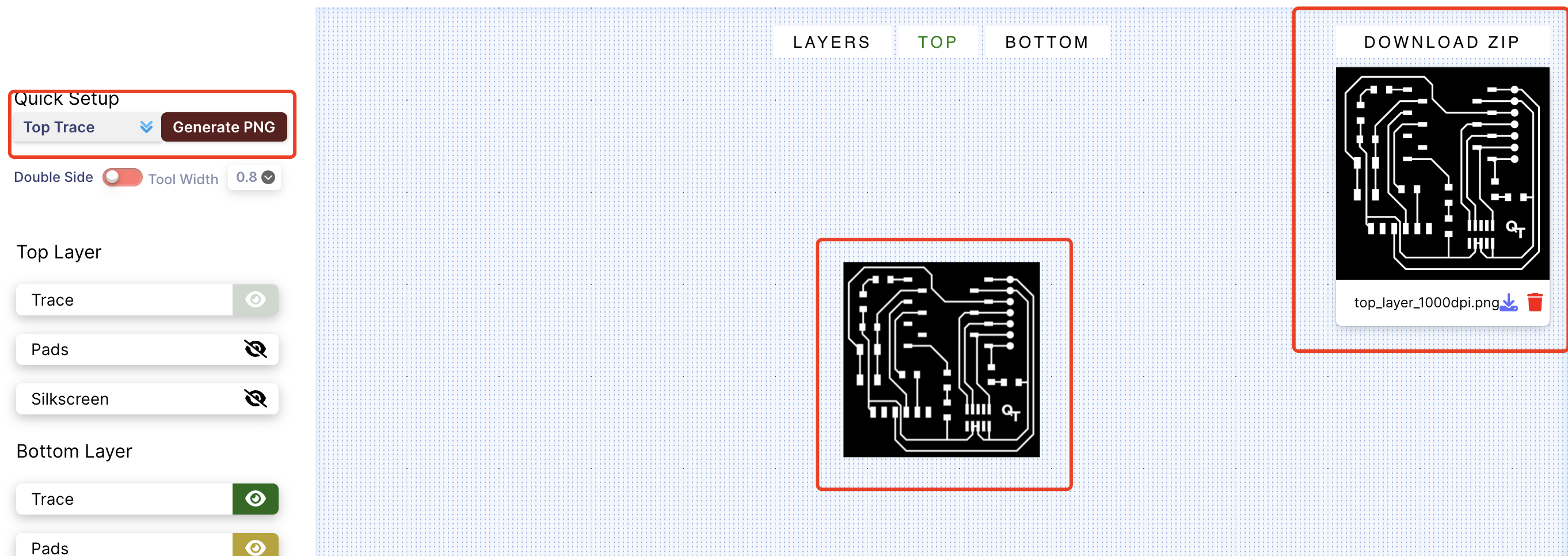
Choose Cut to create outline cut file
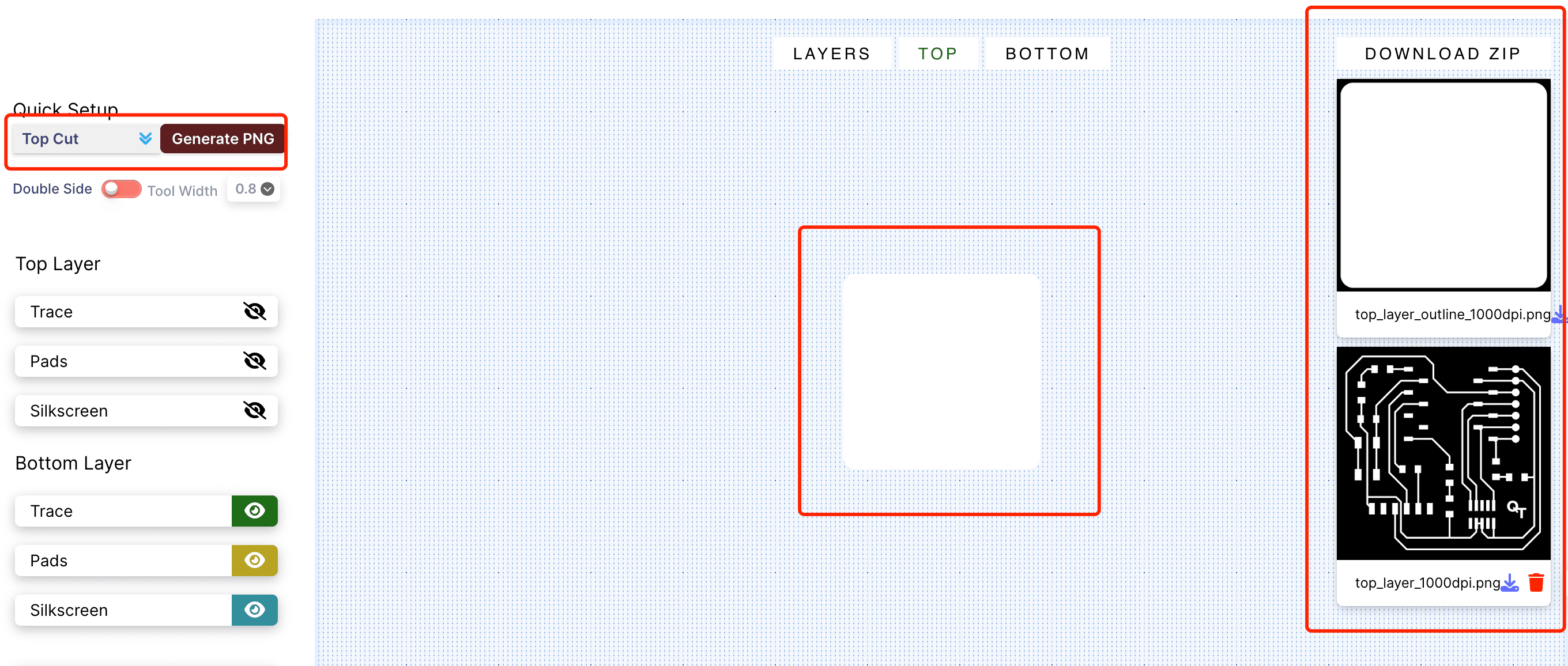
Choose Drill to create outline Drill file
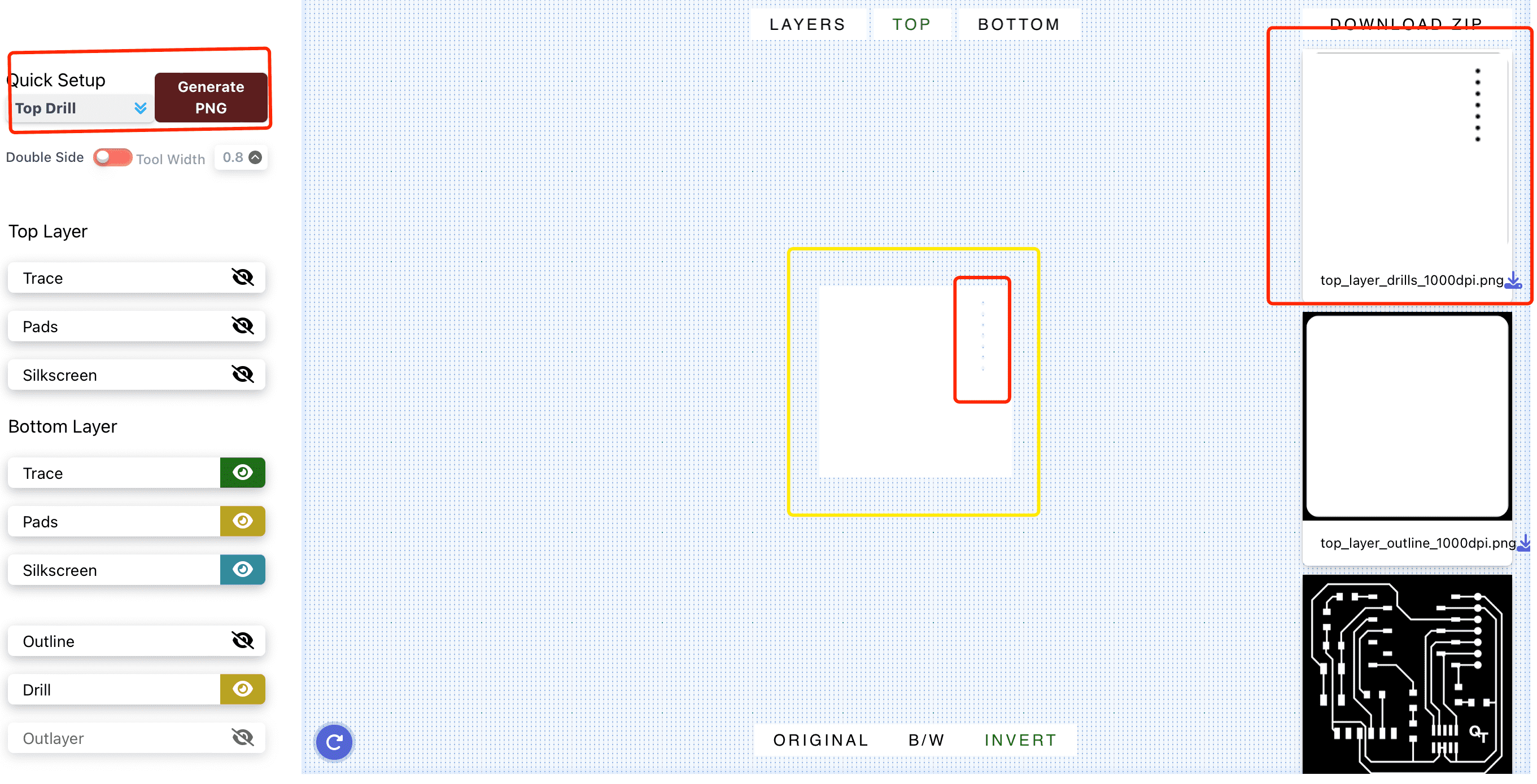
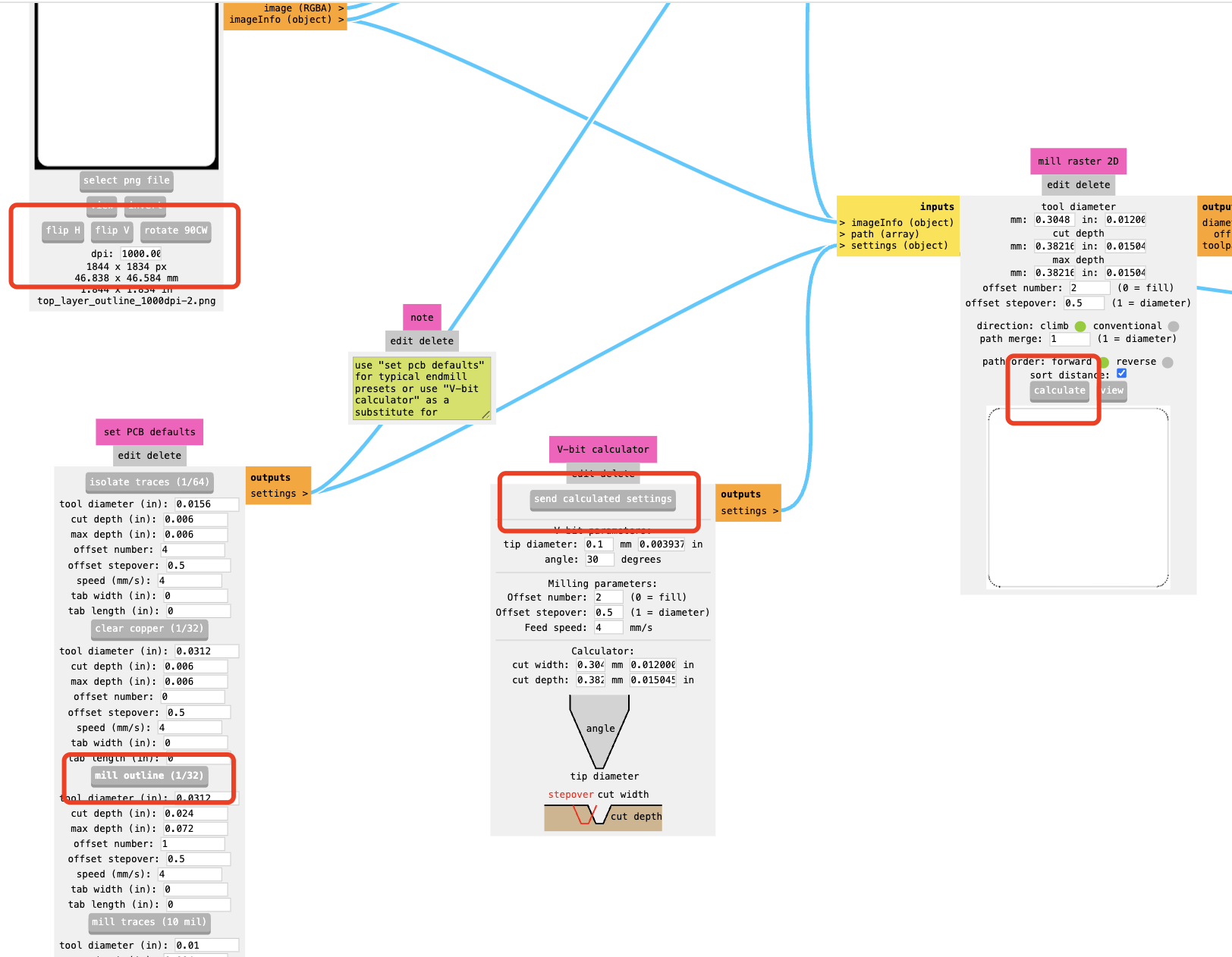
Step 7 Generate the G-code Files using ModsCE
First, open the link as below:
It is needed to generate diffrent G-code files for trace cutting, outline cutting and drill.
For the trace file, the parameter needed to be set are as below
Always remember to set the dpi to 1000
For the v-bit, you can also change the parameter based on the real v-bit you have choosen instead of
using the default parameter to get a better PCB. The V-bit I have choosen 20 20
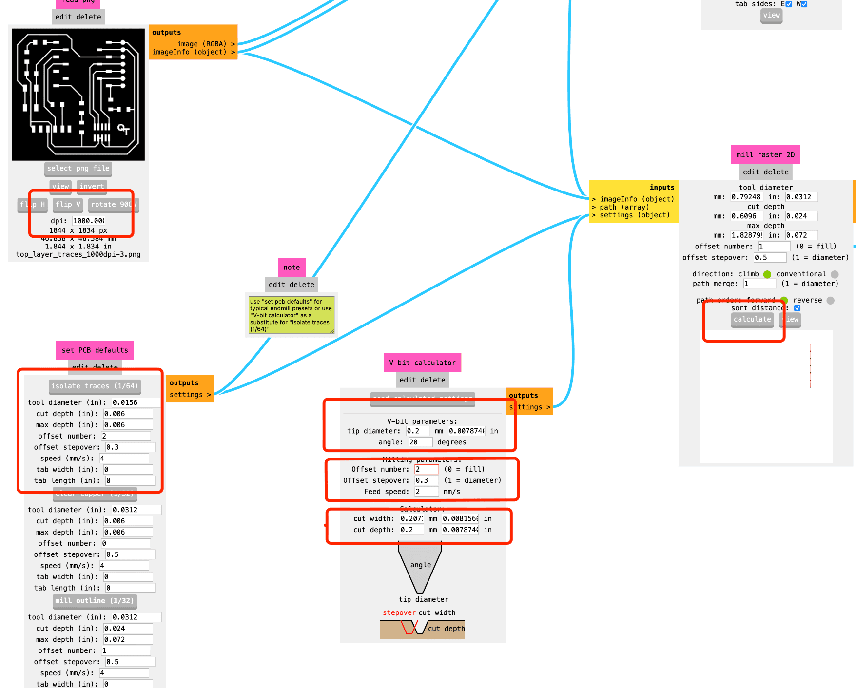
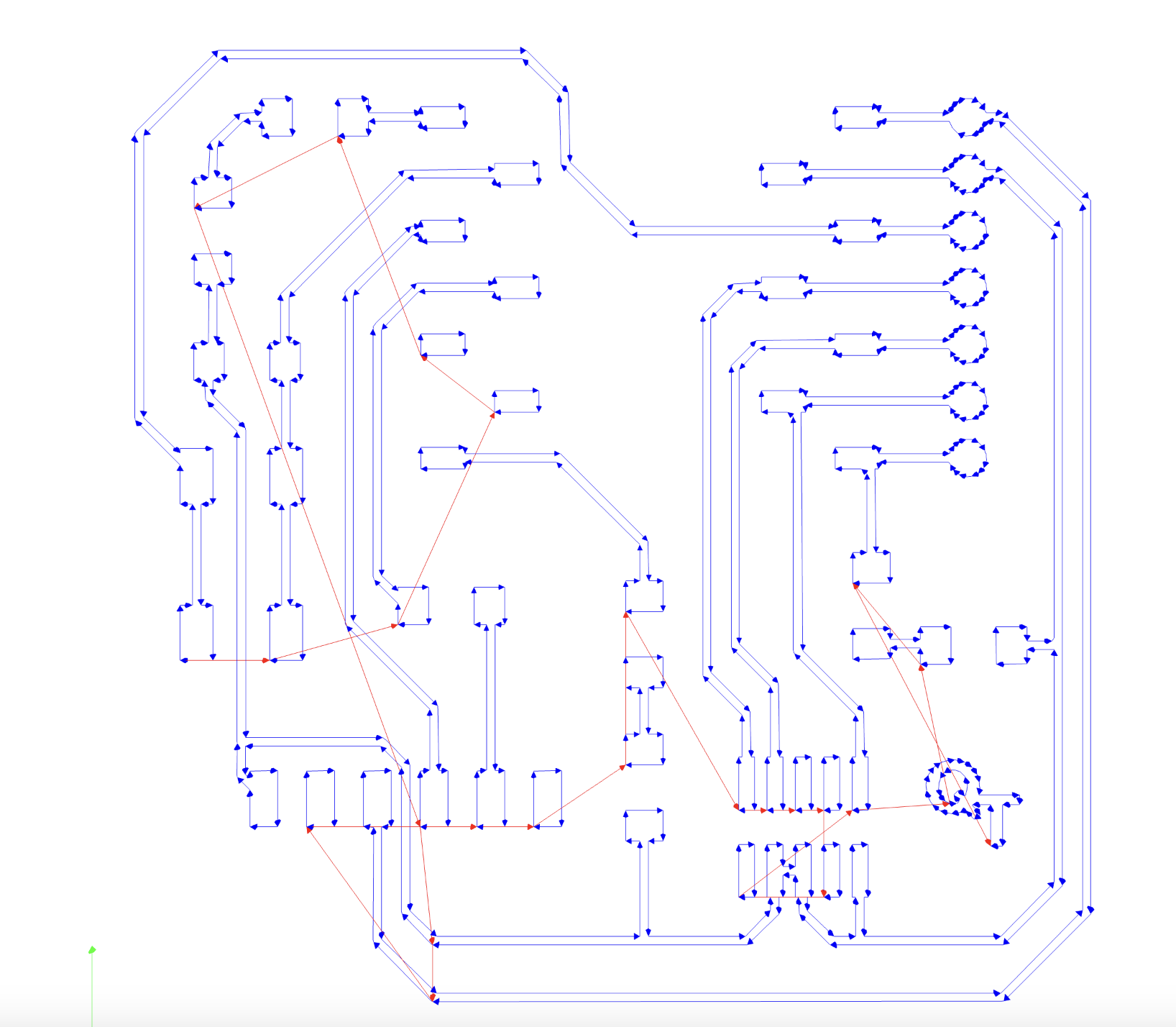
You can also preview the trace of cutting
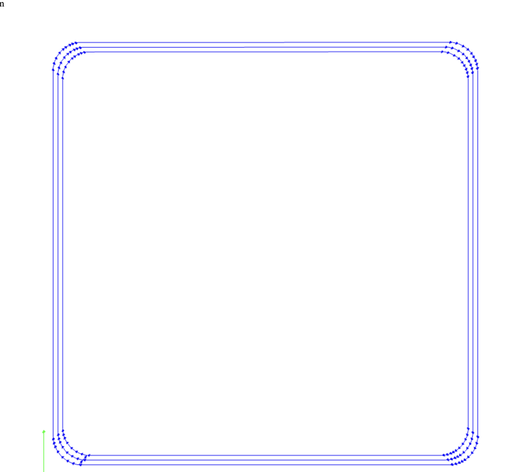
For the outline and drill file, the parameter needed to be set are as below:
Always remember to set the dpi to 1000
use the default parameter is fine.

You can also preview the trace of cutting

PCB Production Procedures Machine Part
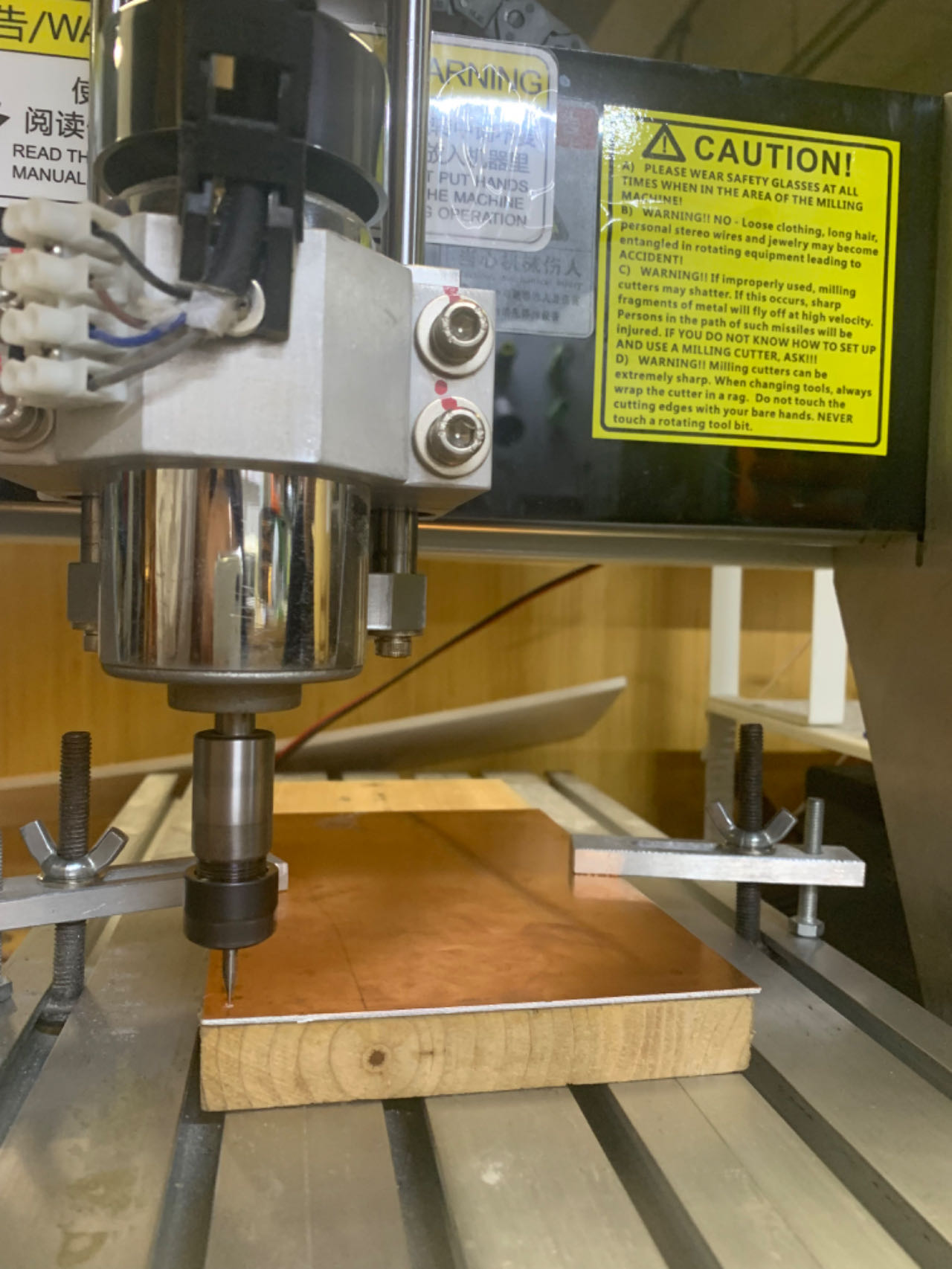
The CNC machine we used at ChaiHuo Shenzhen is as below:

It is very important to get proper training on the operation of the machine before using it!
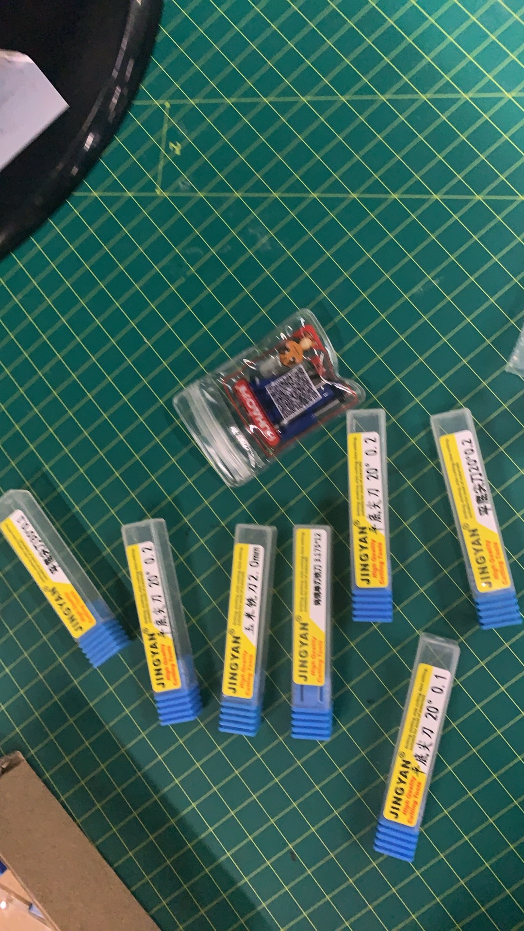
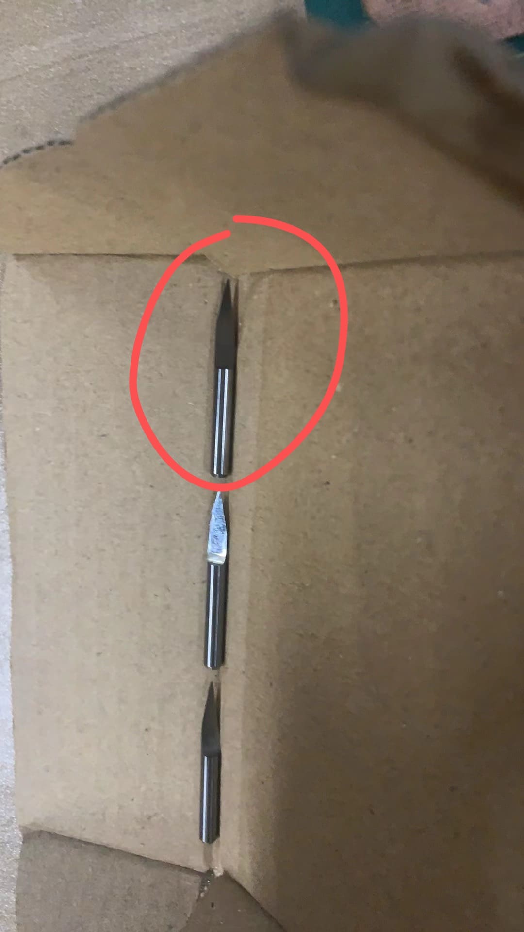
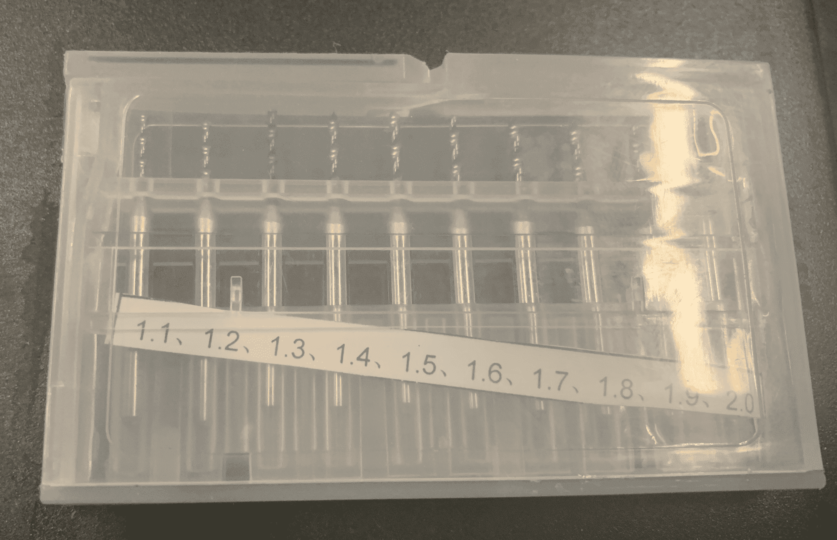
Step 1 Choose the v-bit to cut the trace part of the PCB
I have choosen the 20 20 V-bit to cut relatively thin path.
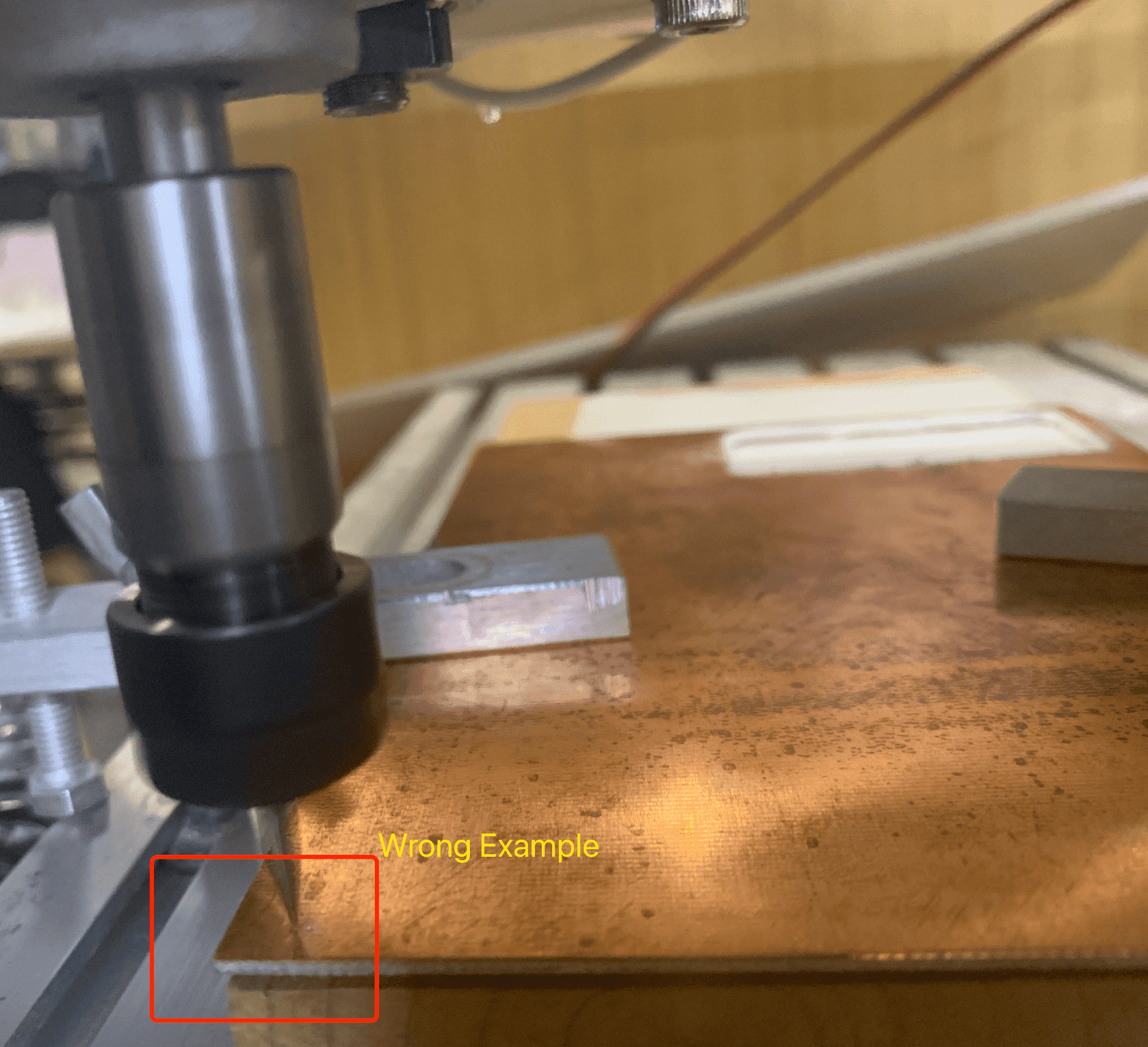
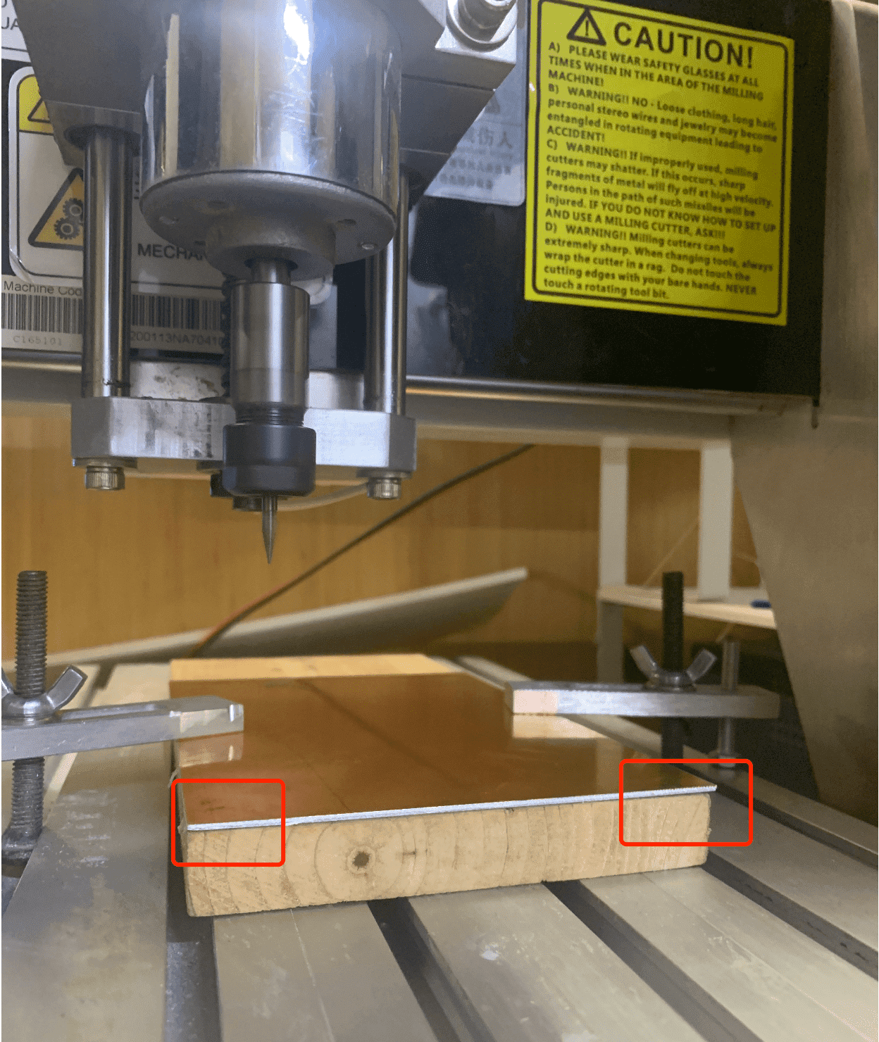
Step 2 Install the V-bit and tape the cardboard to a plywood as below:
It is very important to ensure that the cardboard has no corners curled up, otherwise your PCB will look very unsightly.
Wrong example:
Correct example:
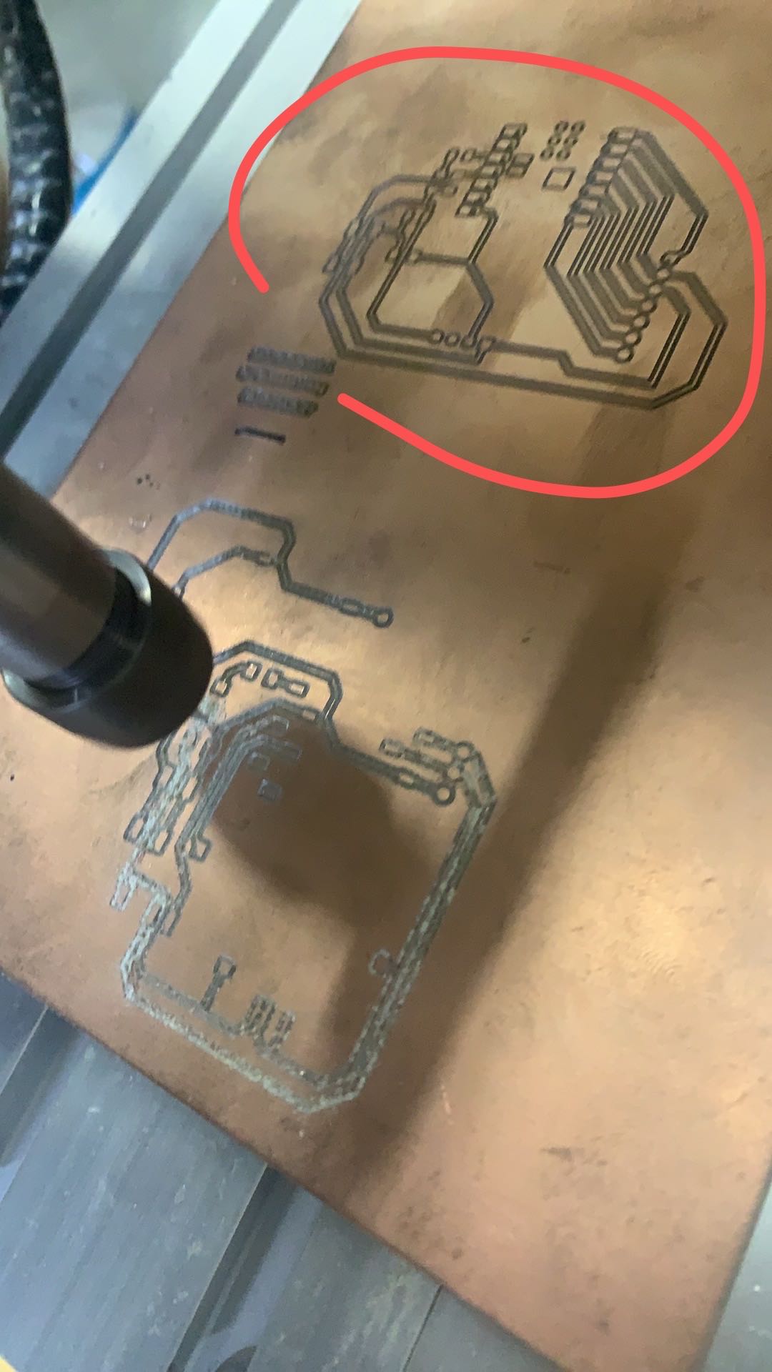
Step 3 Adjust the z-position of the v-bit
This step is also very important, becuase without proper z-position setting, your PCB will be cutted too deep and losing the copper connection wires
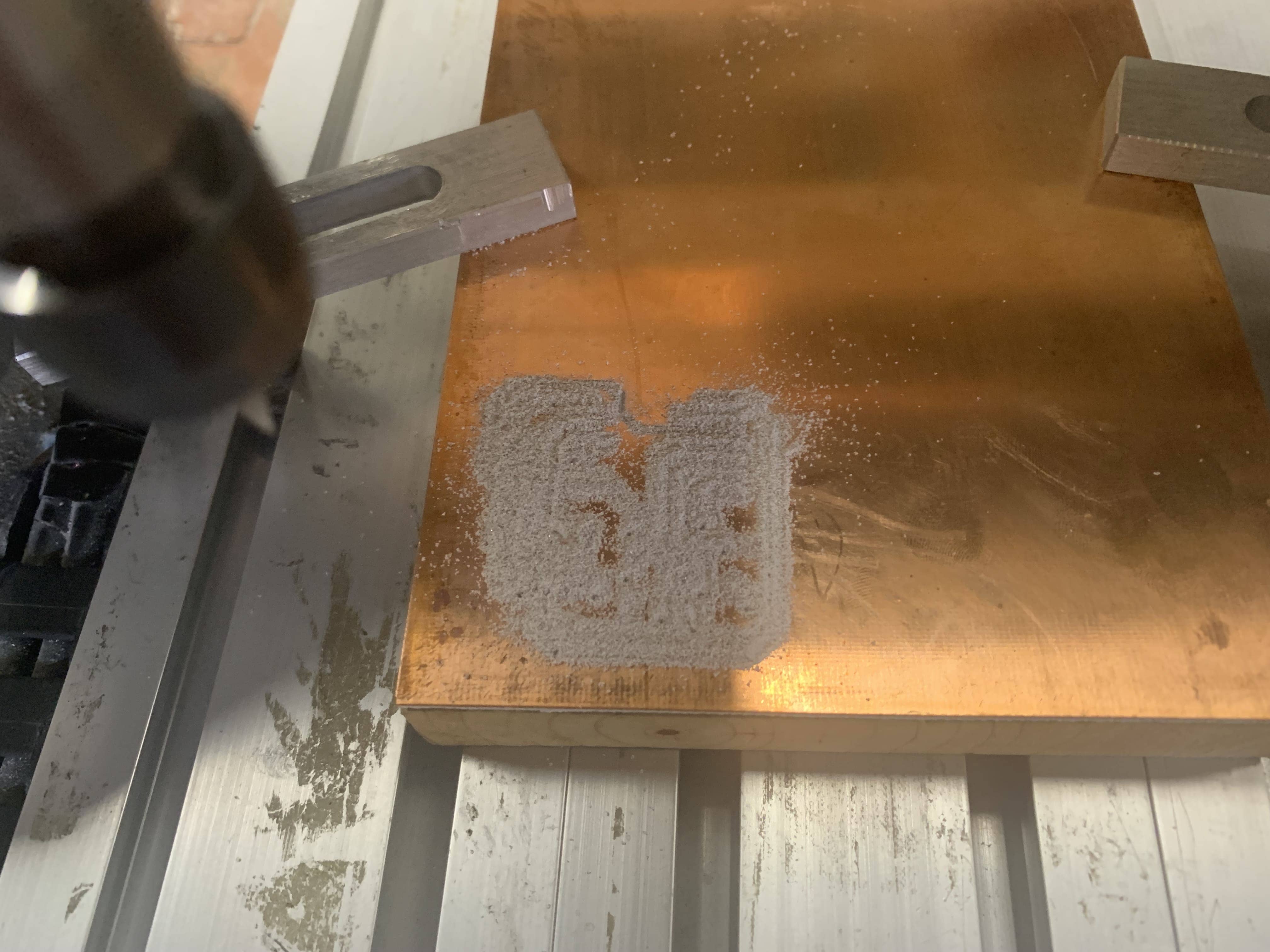
Firstly, I adjusted the z-position according to my hunch
yet the PCB was cut too deep as below:
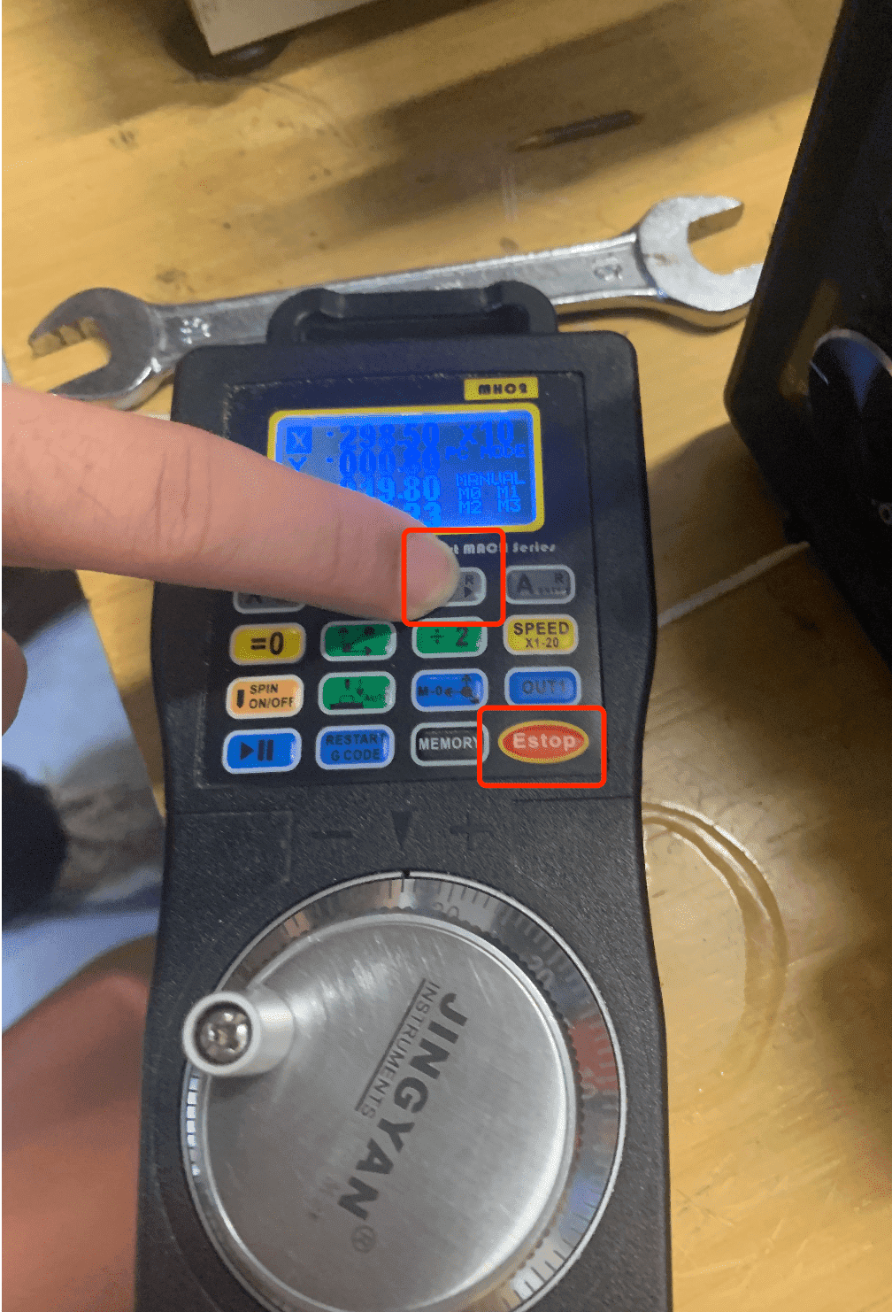
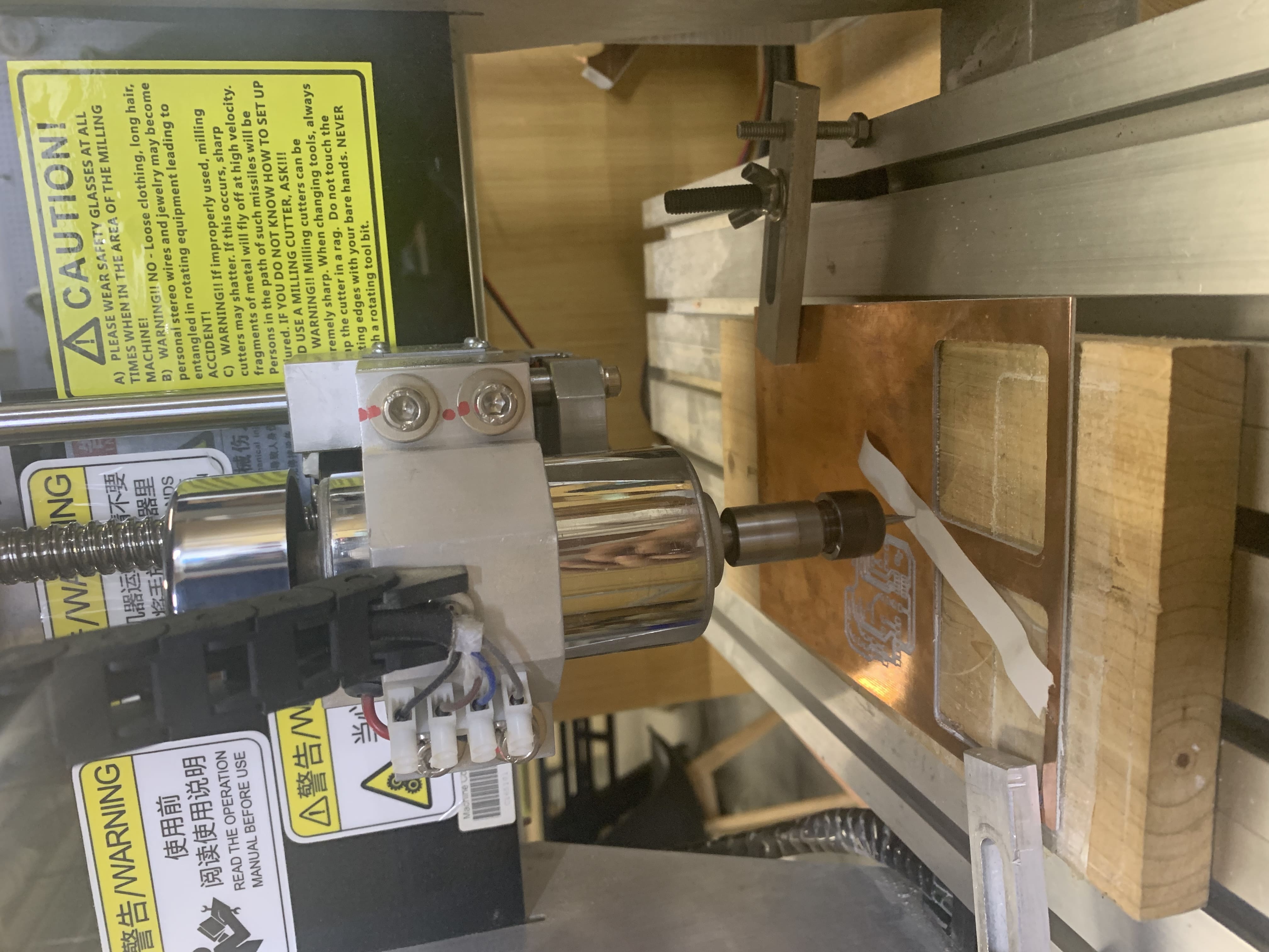
The tool used to adjust z-position
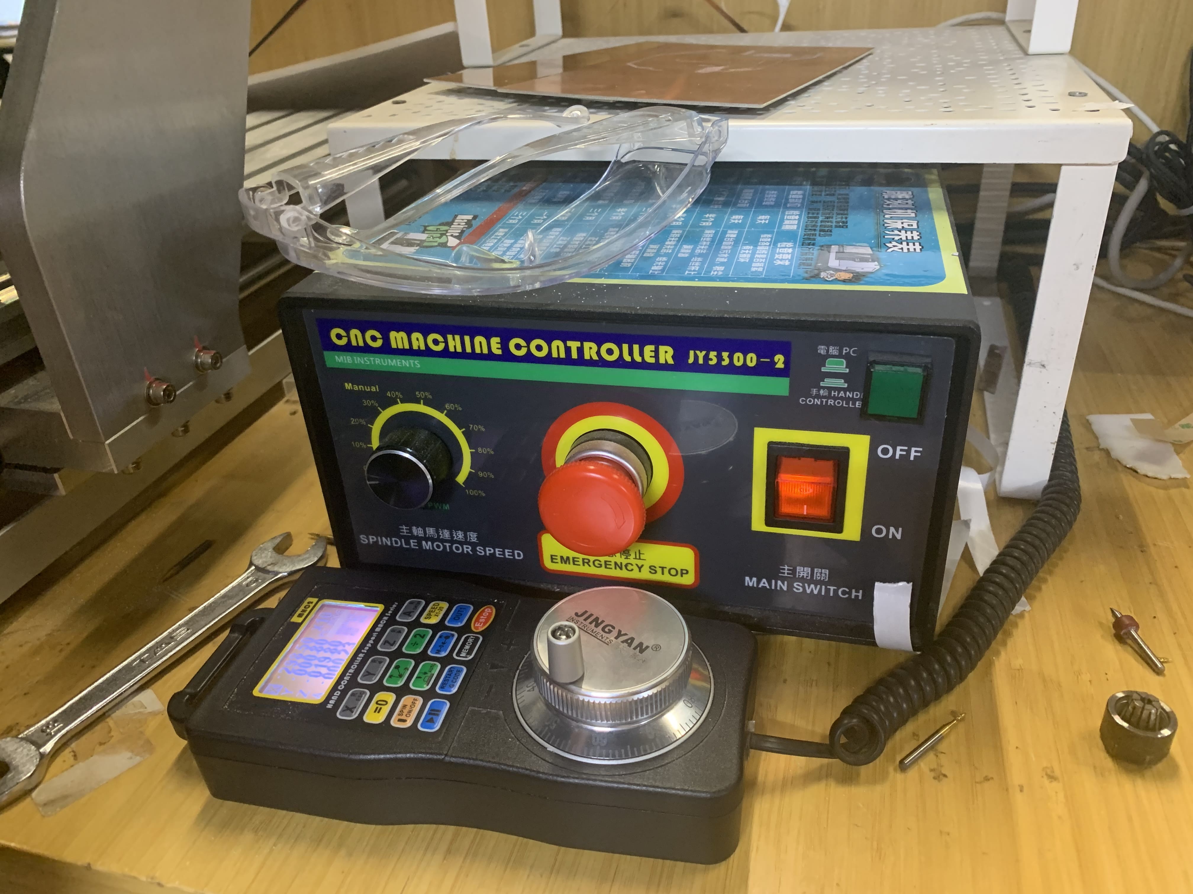
Press "EStop" first,then adjust X, Y, and Z positions
My PCB is cutted too deep because the z-positon is too low.
Secondly instead of using hunch
I Put a slip of paper between the V-bit and the copper plate.
You can sense the distance between the V-bit and the copper plate through the paper.
It should be just right to feel that the V-bit touches the copper plate,
rather than the rotation of the V-bit. If you feel the rotation of the V-bit, this z value will be too deep again.
The z value needs to be adjusted for every 0.1 deviation.
Even a deviation of only 0.1mm can cause the cutting to be too deep.
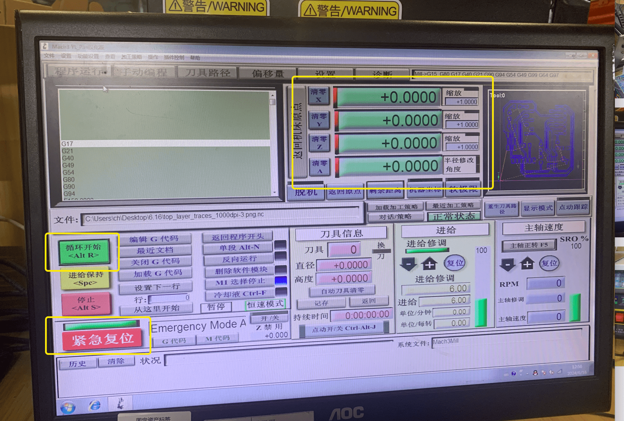
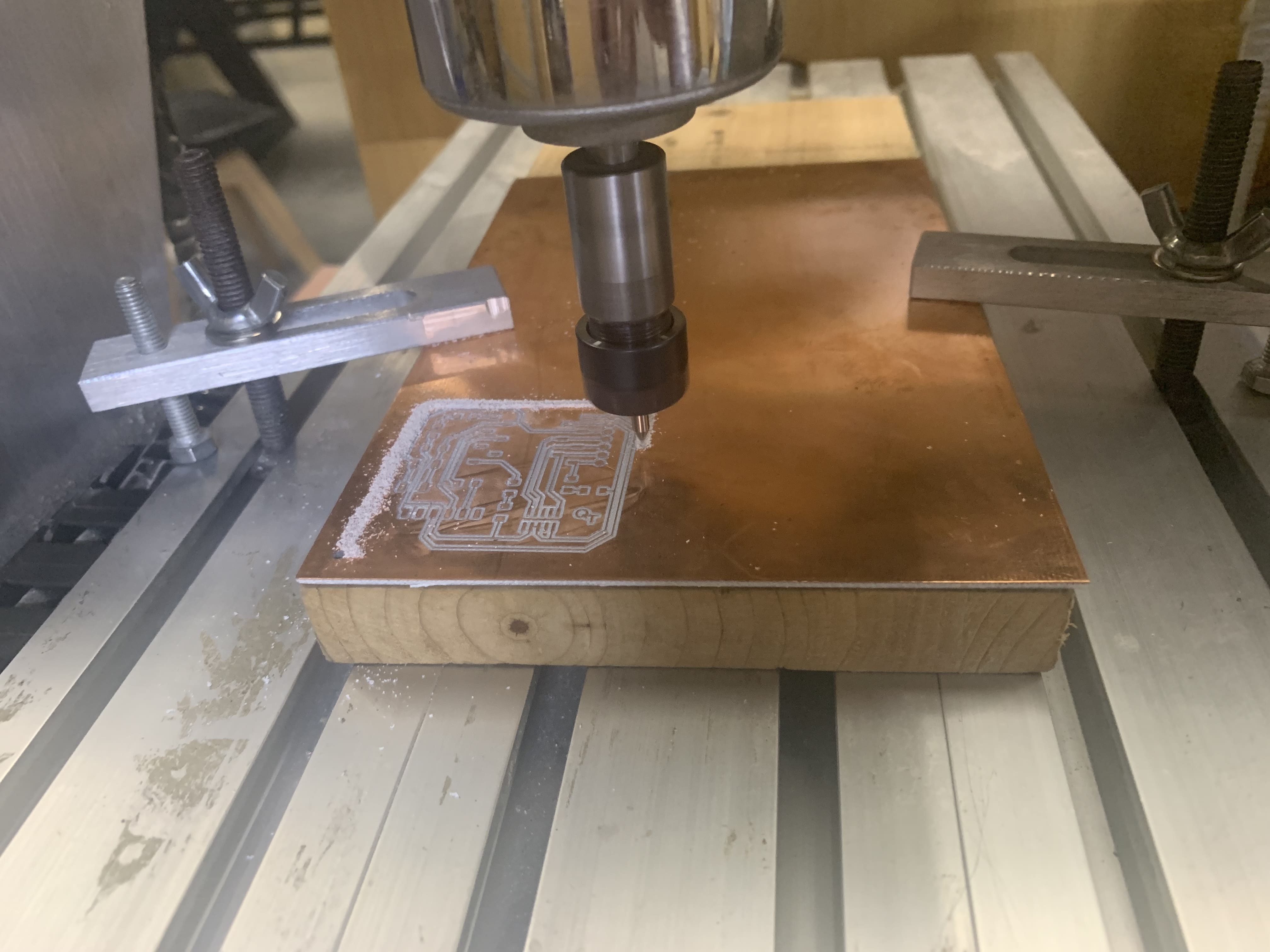
Step 4 Load the files using the software
Load the file in the software and after the position of the v-bit is fixed.
Set all the parameter of X Y Z to zero.
Then start cutting.
Step 5 Start Machine Cutting
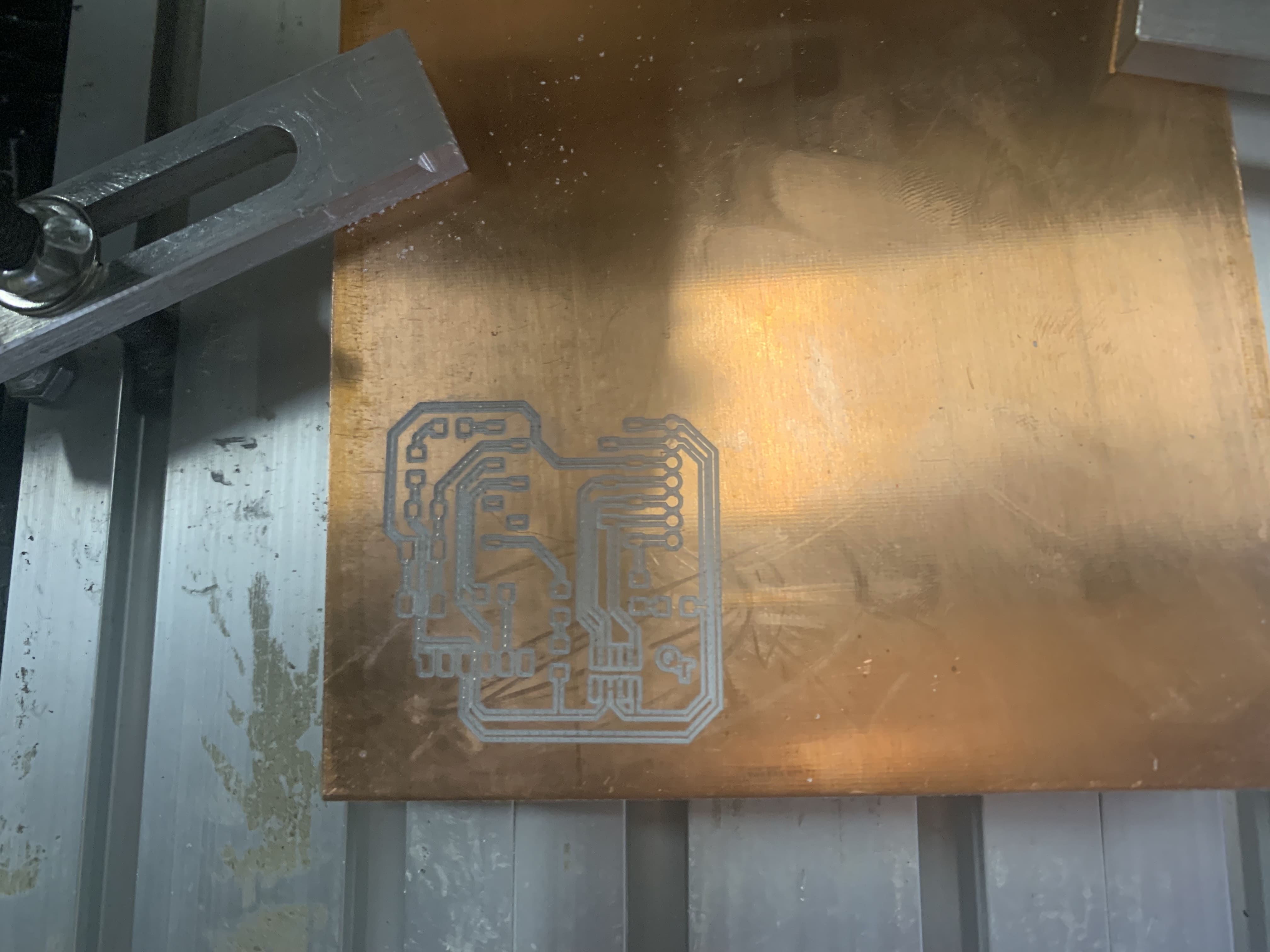
Step 6 The trace cutting is finally finished.
Step 6 Change the v-bit to endmills
Step 7 Cut the outline
To cut the outline is relatively easier, it is fine to set the mills deep
Then start cutting.It will cut three rounds and each round the mills will go deeper.
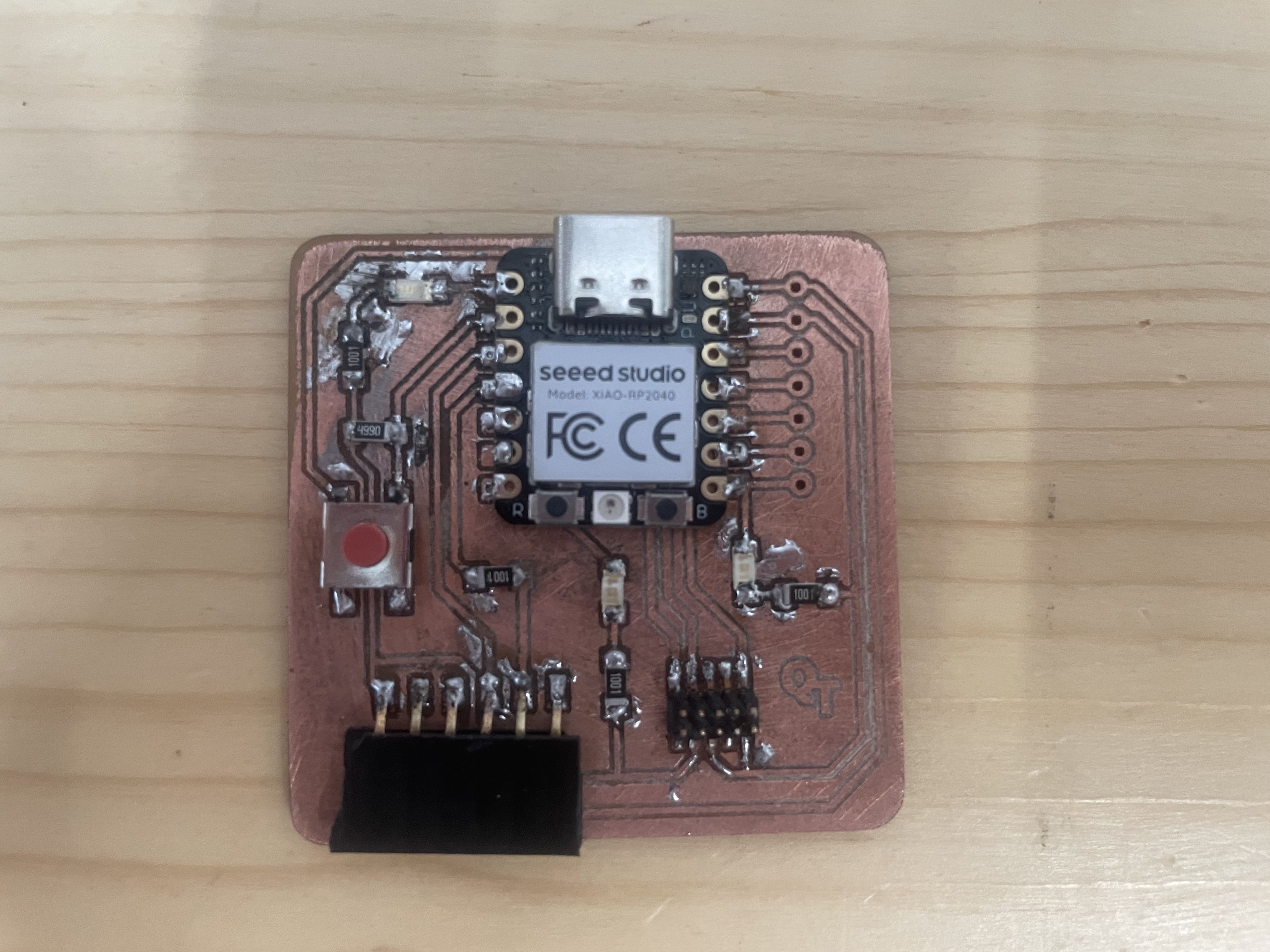
Step 8 Finally, the PCB is ready!
After the PCB is ready:
- Gently sand the PCB surface using fine-grit sandpaper (600-800 grit) to remove any excess copper flakes.
This will help prevent short circuits. Take care not to over-sand and damage the copper traces.
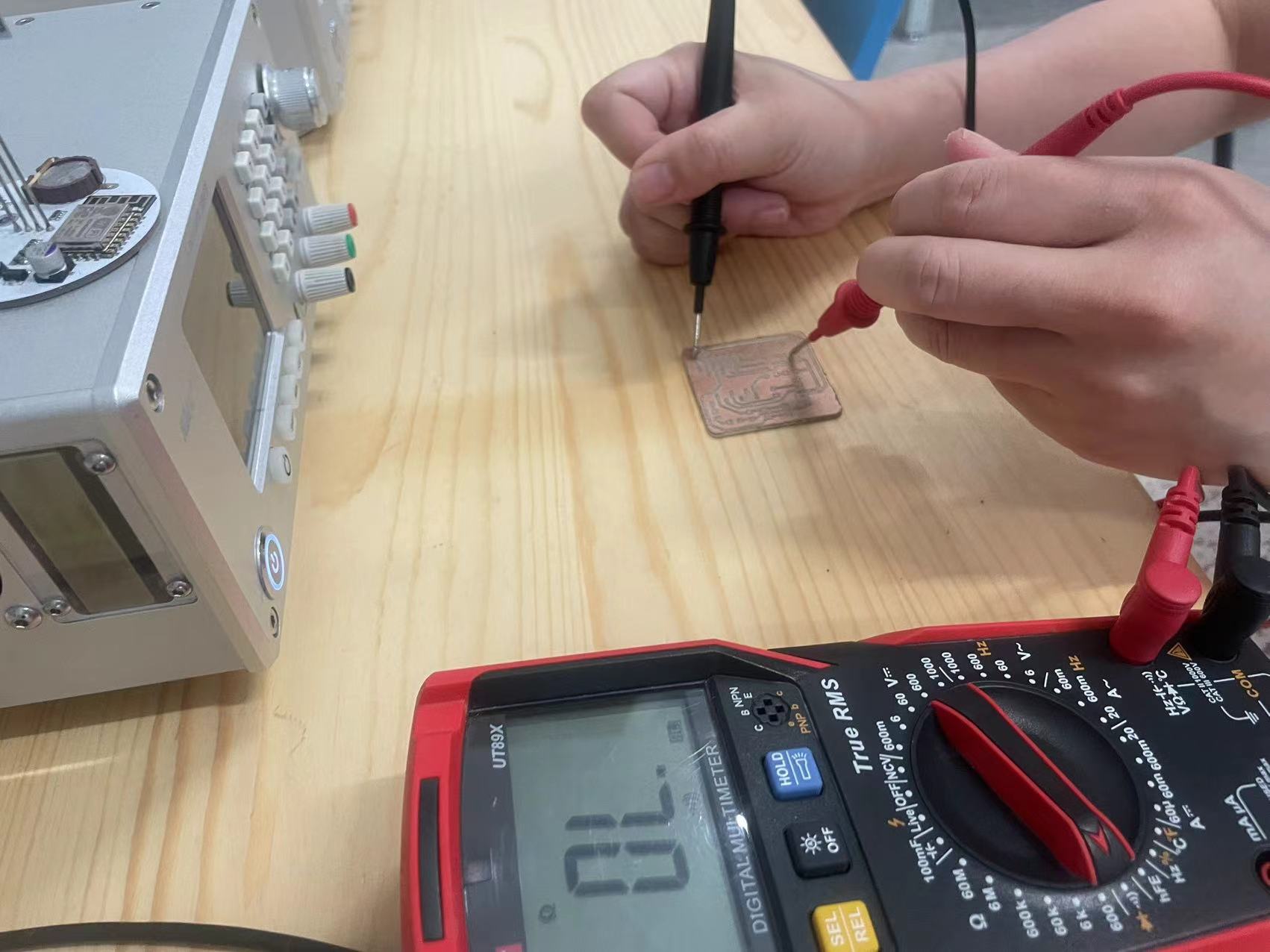
- After sanding, carefully test all the connections on the PCB using a multimeter to ensure there are no breaks in the circuit paths.
- If you find any broken connections, you can use solder to re-establish the connections.
For short circuits caused by improper layout, you may need to carefully cut away the shorted section and then re-solder wires to fix the issue.
Solder PCB
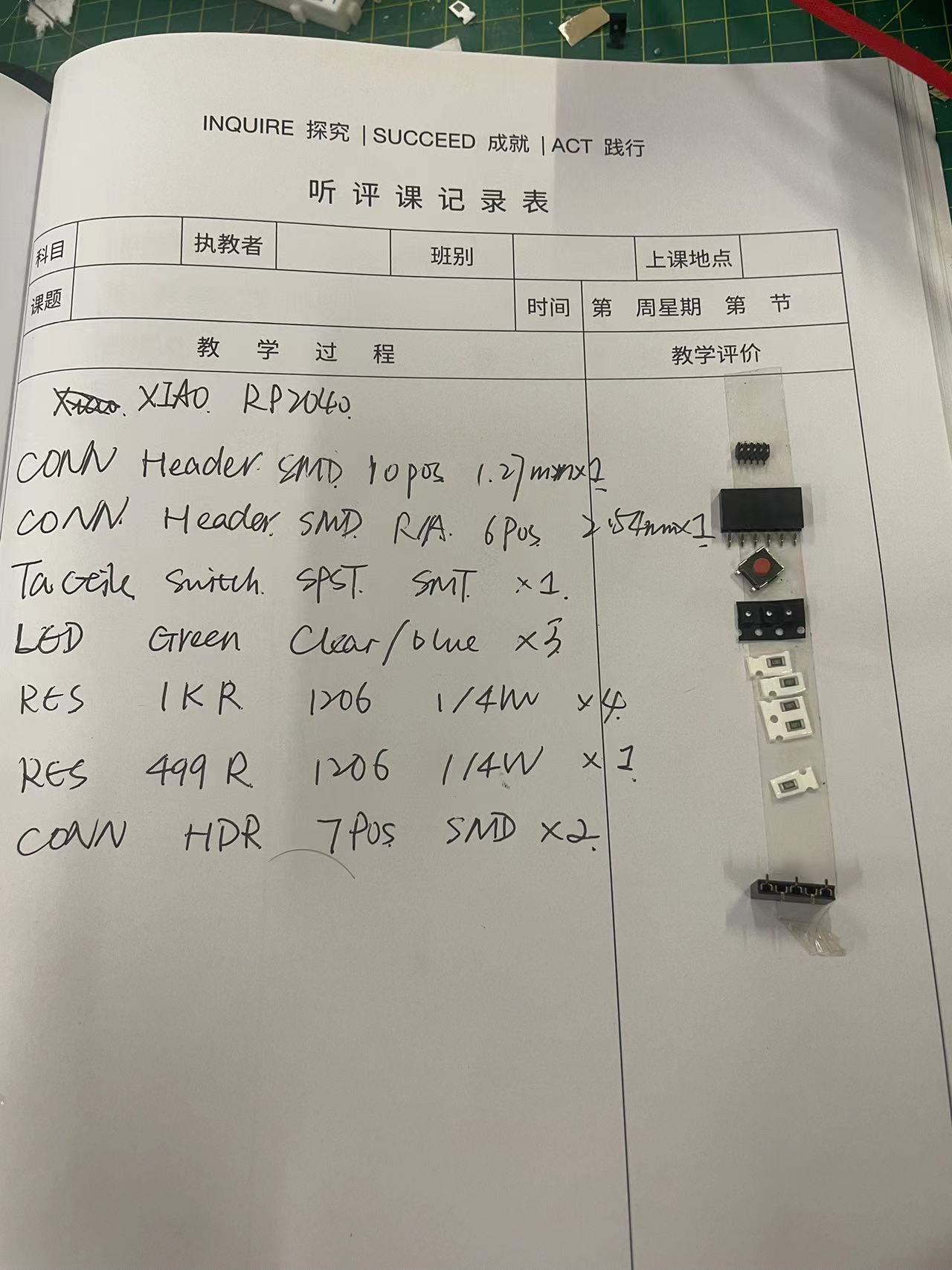
Step 1 Get all the Components Ready
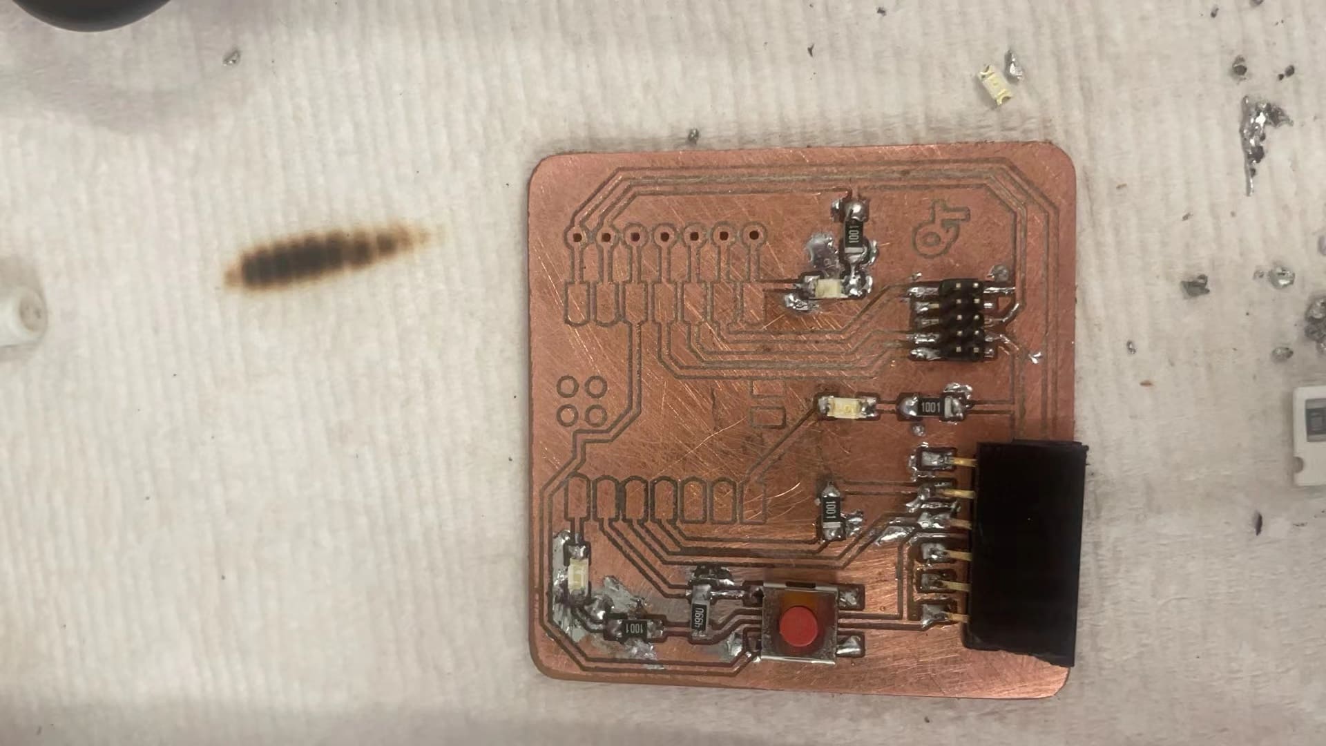
Step 2 Solder the Components
Tips for soldering:
- Solder From the small ones like the LED or resistor.
- If the solder ball is too large, you can spread it to other areas of the board. But at this time, it is necessary to ensure that the spread solder does not short-circuit the insulation path next to the copper wire.
- FOR EACH COMPONENT SOLDERED, IT IS NECESSARY TO IMMEDIATELY CHECK WHETHER THERE IS A SHORT CIRCUIT AND CORRECT IT IMMEDIATELY.
- IF UNFORTUNATELY THERE IS SOLDER CAUSING A SHORT CIRCUIT, SPEAD THE SOLDER TO MAKE THE WAY CLEAN or CUT THE CIRCUIT WITH A KNIFE carefully.
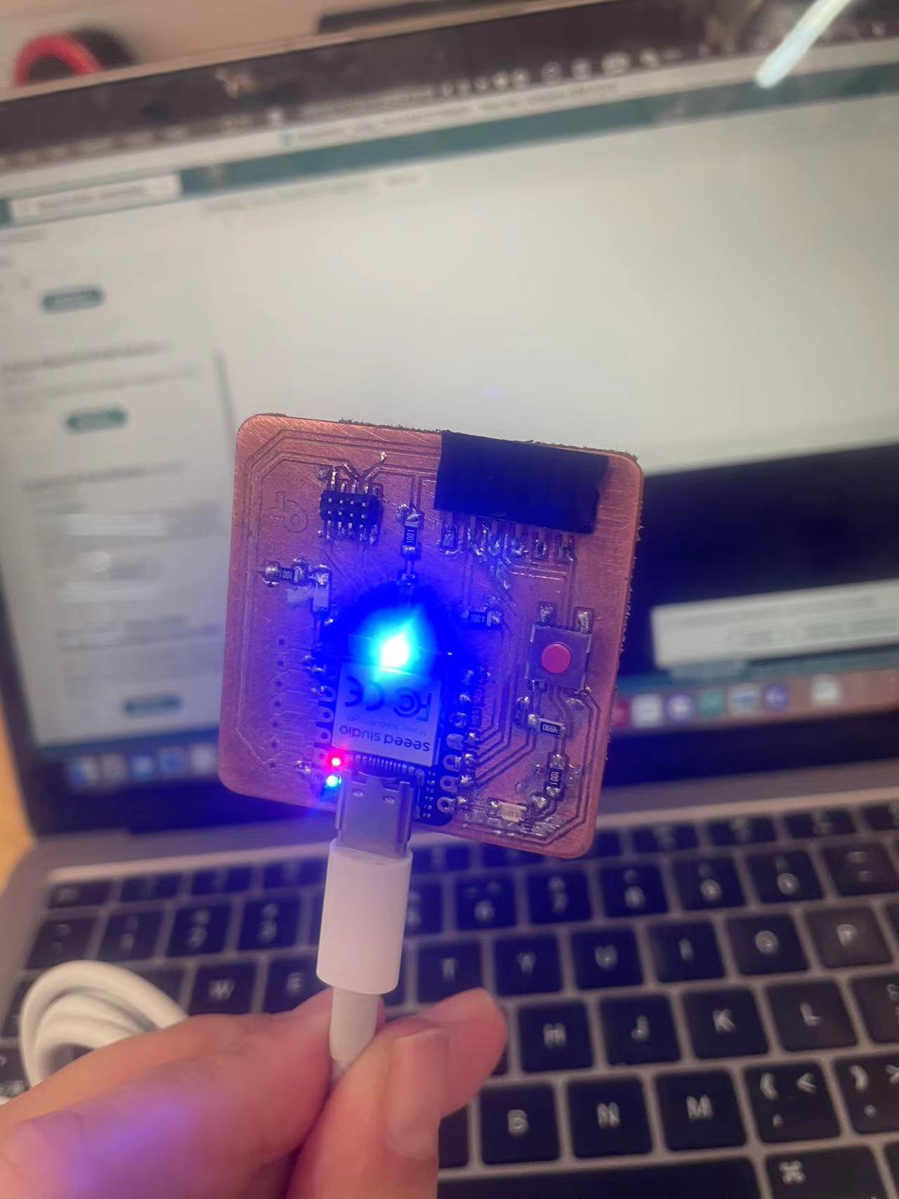
You can see that although my soldering is extremely ugly, there is no short circuit anywhere.
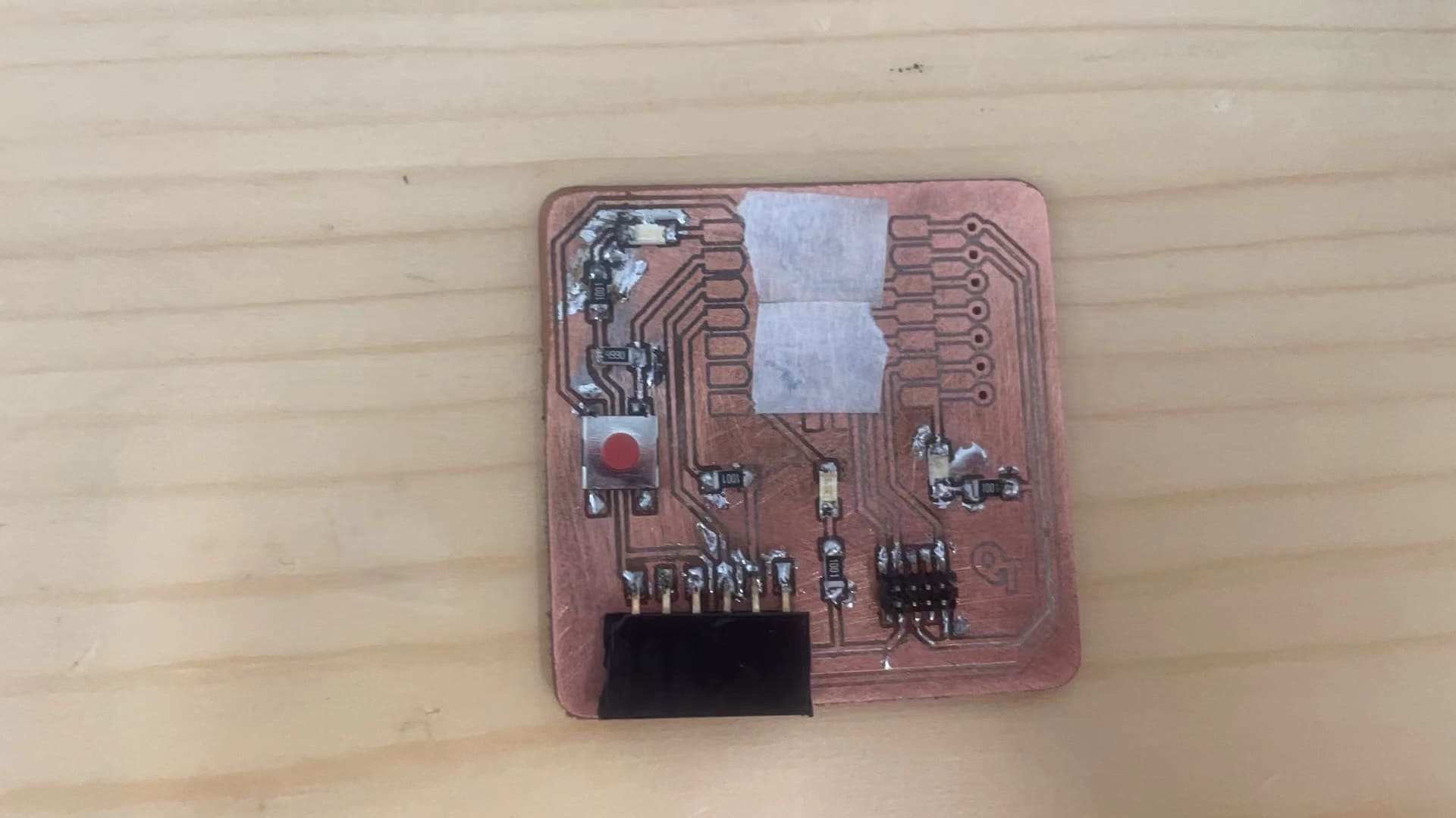
Step 3 Tape it
It is necessary to seal the contact area between the microcontroller and the PCB board with tape to prevent short circuits.
Step 4 Solder the MicroController
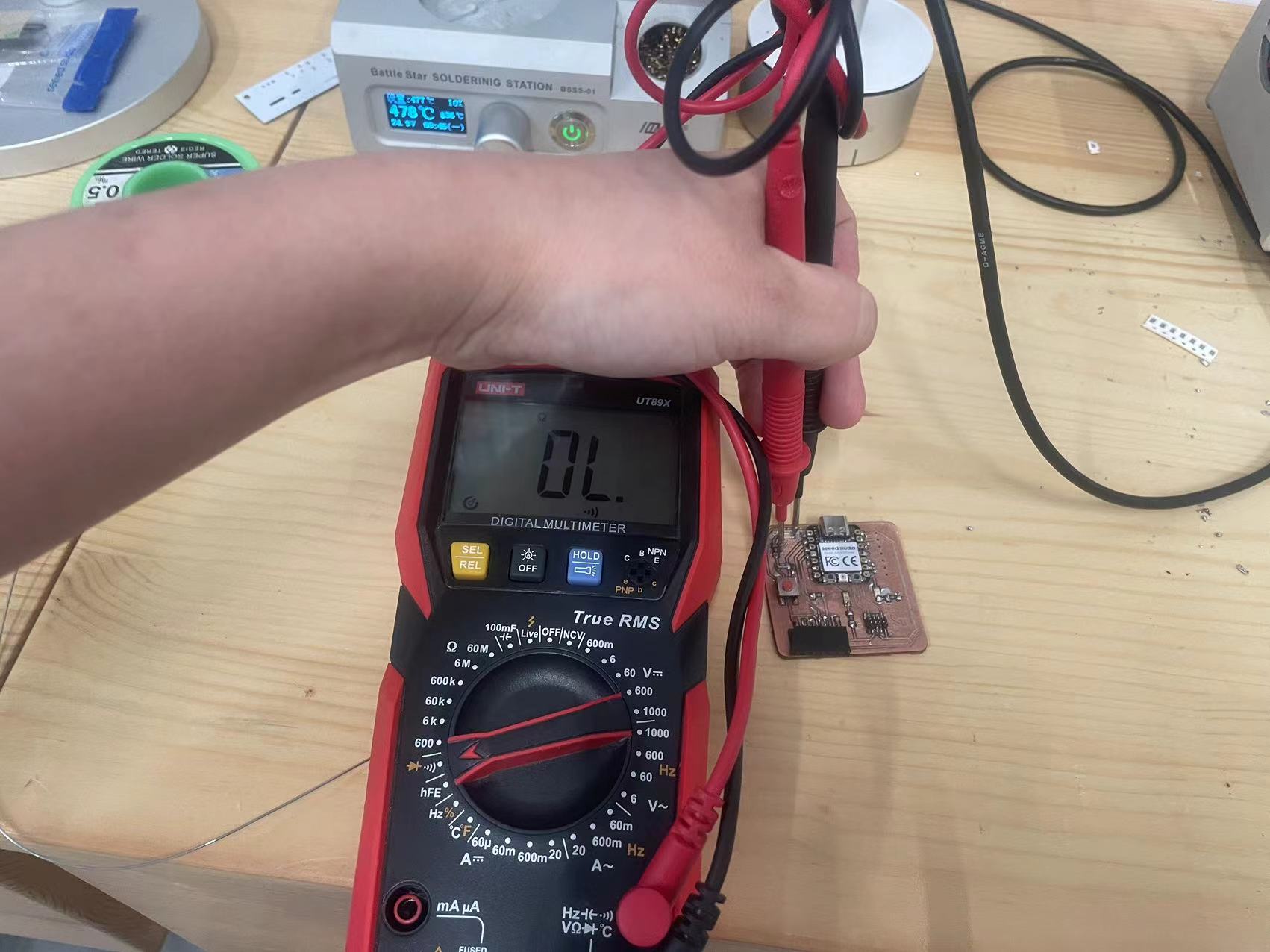
Step 5 Test
Test all the pins to see if they are correctly connected and no short circuit happens。
Step 5 Blink!