8. Electronics Production
This week I started to work on Electronics Production to make a printed circuit board with a micro-controller using a CNC milling process, stuffing & soldering of the PCB as well as to test & verify the circuit board if it works. I have also learnt on how to fabricate my first Printed Circuit Board using StepCraft CNC Milling Machine while the group assignement is to characterize the design rules for our in-house PCB production processes and document the work as a group or individual.
You can access the group assignment HERE.
Printed Circuit Board Production - StepCraft CNC
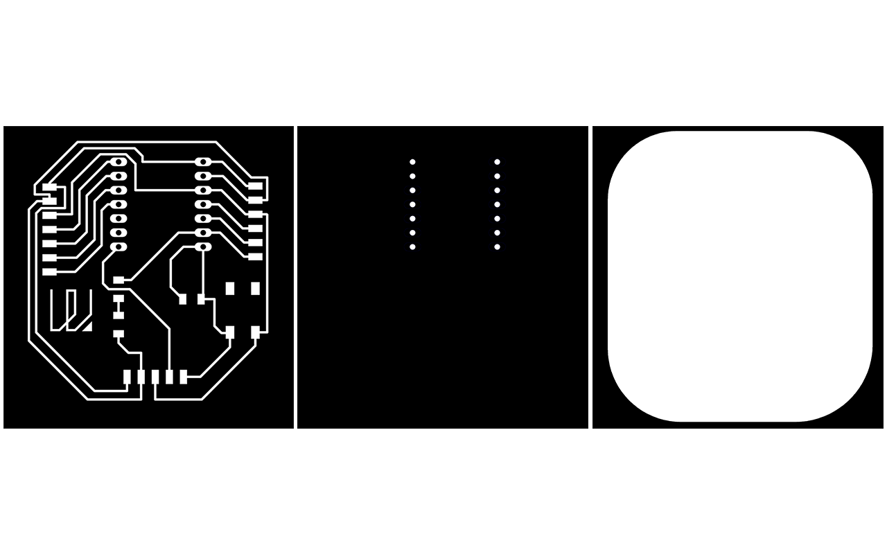
For this week assignment, I am going to produce and fabricate my first printed circuit board (PCB), a continuation work in progress from week 6. which is Electronics Design. During week 6, I have already create my printed circuit board using Autodesk Fusion 360/Eagle and have them exported into PNG images files which will then be send to the MODs online program to generate the G-Code. Below are the PNG files of my printed circuit board design.
You may download all the 2D PNG & NC file HERE.
After generating all the PNG files of my PCB design, I will need to send it to the MODs online program to generate the G-Code. The steps are the already mention in week 6. Electrionics Design so I shall not elaborate further. The most important point is to adjust the parameters of the MODs program so that we are able to CNC mill the board. The parameters adjustment that are important are as follow:
- Mill Traces - By Default, the Mill Traces is 1/64 and this is for the milling of the circuit path. (Remeber to select this for milling the path!)
- Milling Outline - By Default, the Mill Outline is 1/32 and this is for the milling of the circuit board and holes profile. (Remeber to select this for milling the circuit board and holes!)
- Cut Depth - This is the depth of each mill and for Mill Traces, the depth should be around 0.05mm while Mill Outline, it should be around 0.35mm
- Max Depth - This is the maximum depth you want to mill and for Mill Traces, the depth should be around 0.05mm while Mill Outline, it should be around 1.68mm(Thickness of the Copper Board)
- Offset Number - This is number of times of milling path and for Mill Traces, the offset number should be 3 times while Mill Outline, it should be only 1 time
- Cut Speed - This is the speed of the CNC router and by default, it should be at 60 rpm
- Specific Speed - You may adjust the specific speed that your machine is running, i.e my StepCraft CNC is running at 12,600 rpm so I am using 12,600 rpm instead of 11,000 rpm or 12,000 rpm.
- Format & Rate Units - Remeber to select the correct Format & Units that you are using for the milling i.e 60 rpm = 1 rps
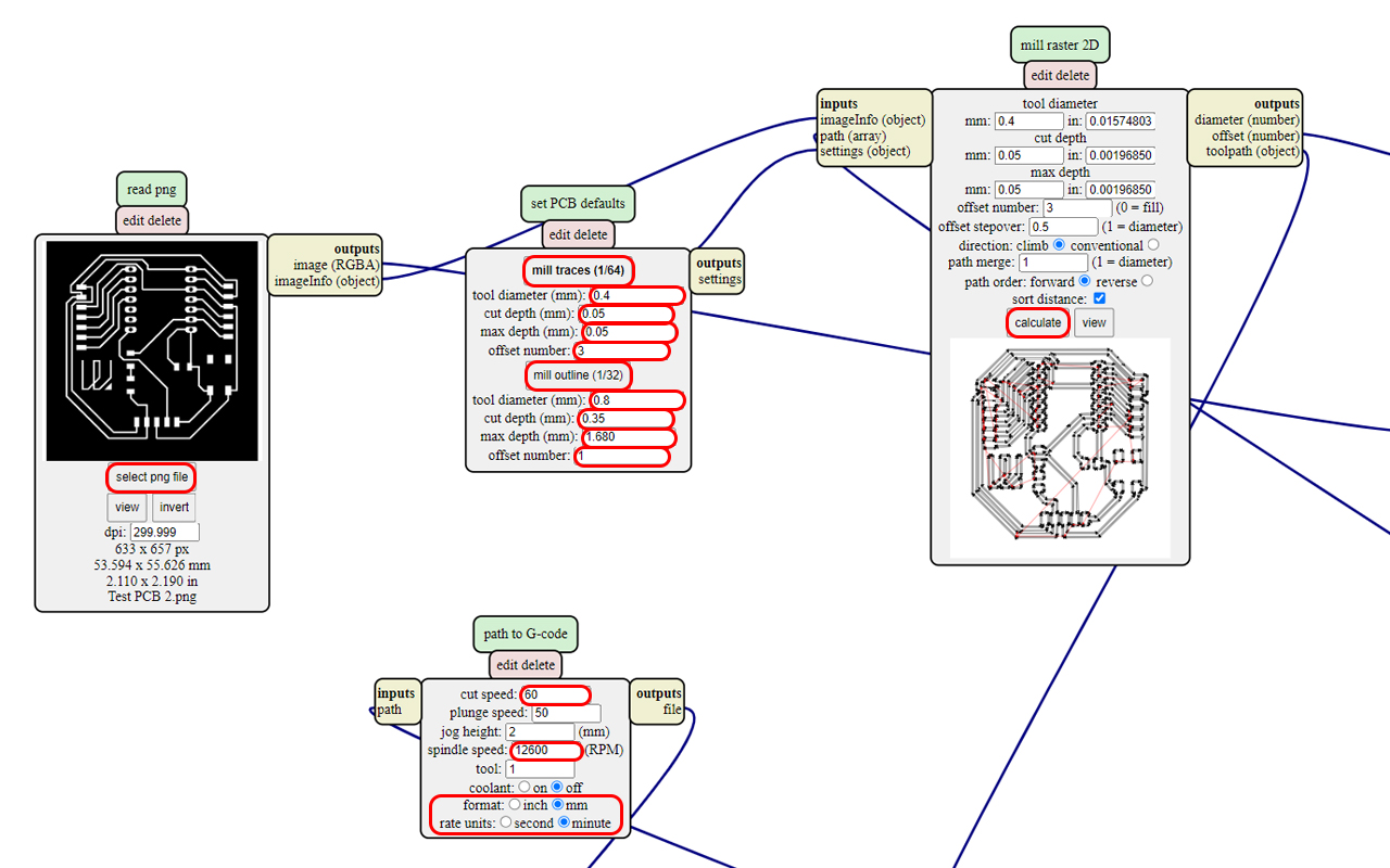
The rest of the settings should stick to default values but you may change it further if you know exactly what you need. The next step is to select the Calculate button and the PNG NC Path image will be generated which will be automatically downloaded. You will then need to safe the files and send it to the CNC milling machine to start milling the circuit board, so in my case, I am using the StepCraft CNC Milling Machine to mill my PCB.
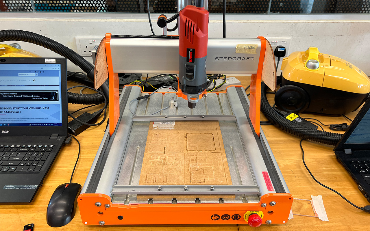
Next, we shall move over to the StepCraft CNC Milling Machine and prepare the settings. The steps of preparing the machine is very similar to the milling machine that I had used for the milling of the coffee table and the basic steps are mention below in sequence:
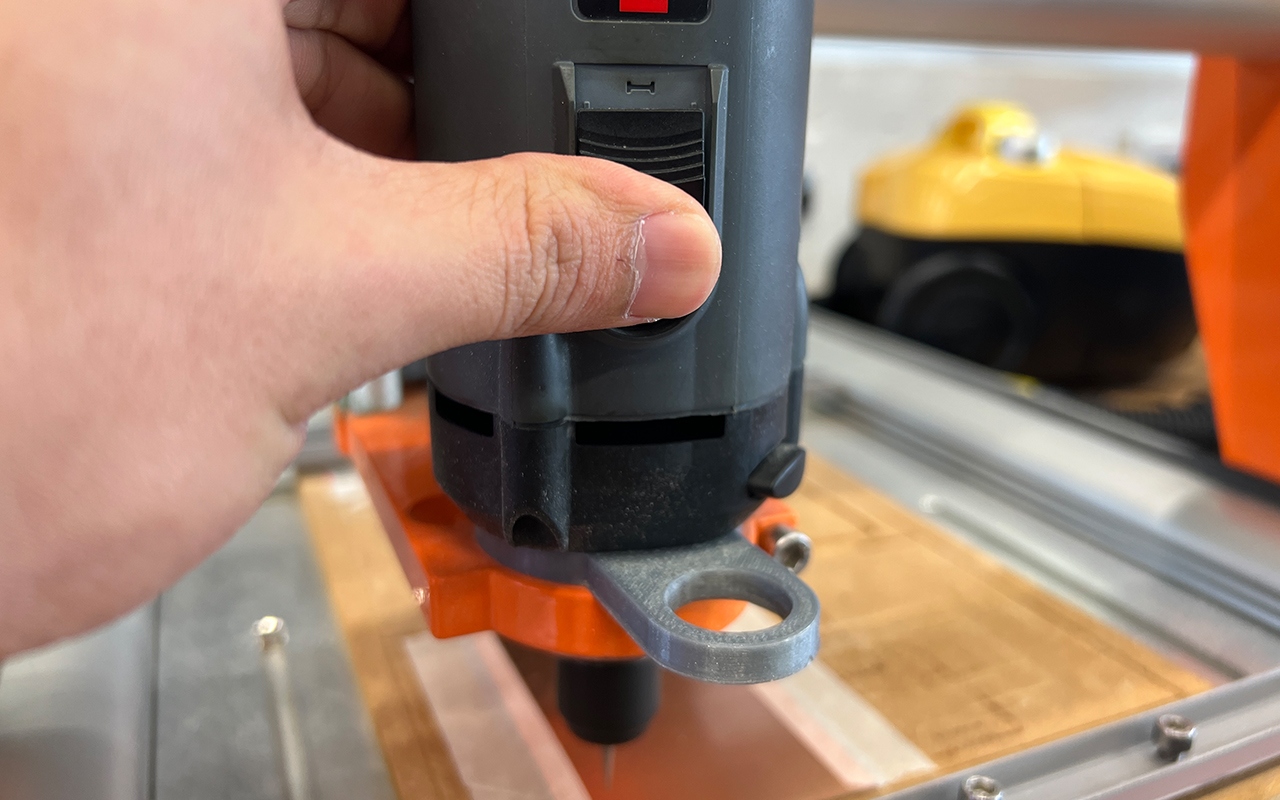
- Prepare the milling bit
- Prepare the milling bed (Material Stock)
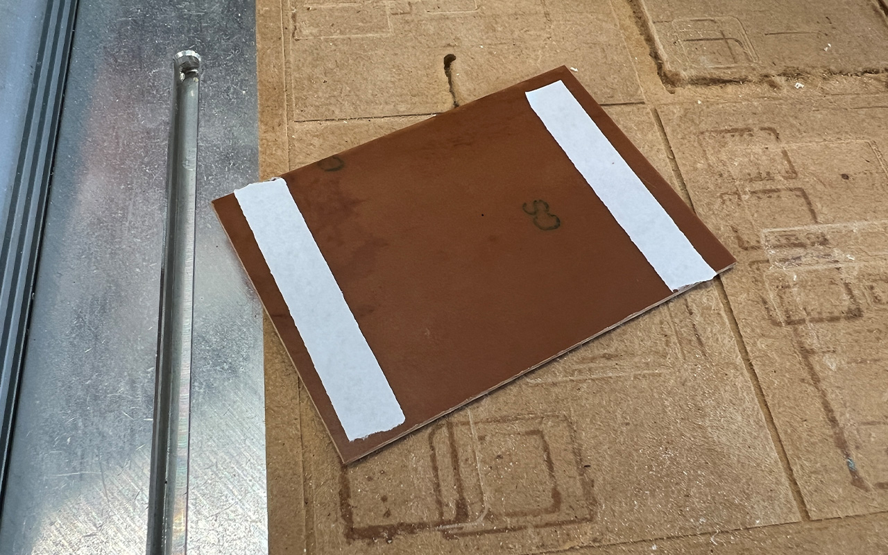
- Paste the Copper Board on the milling bed with double-sided tapes
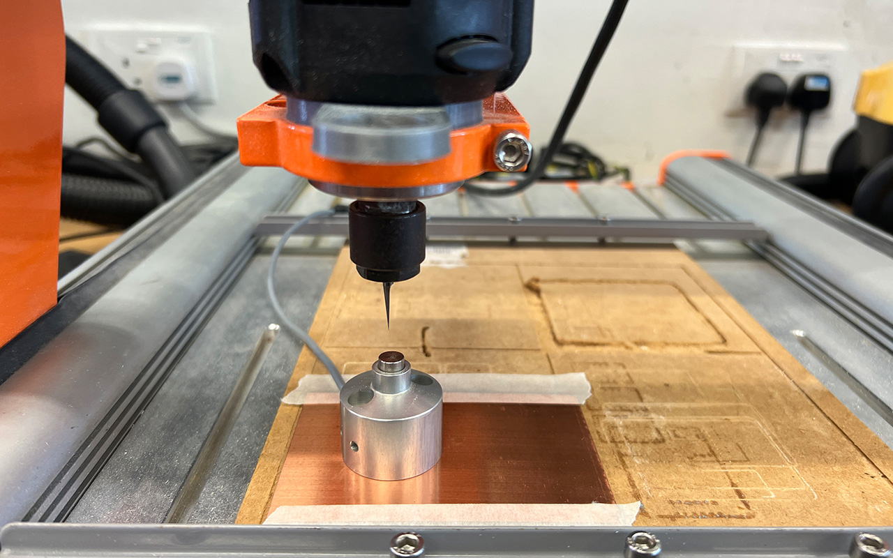
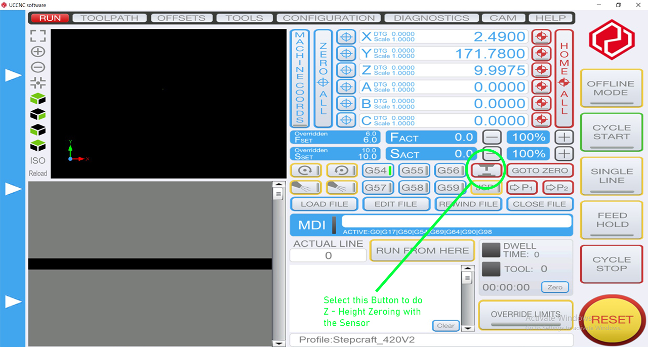
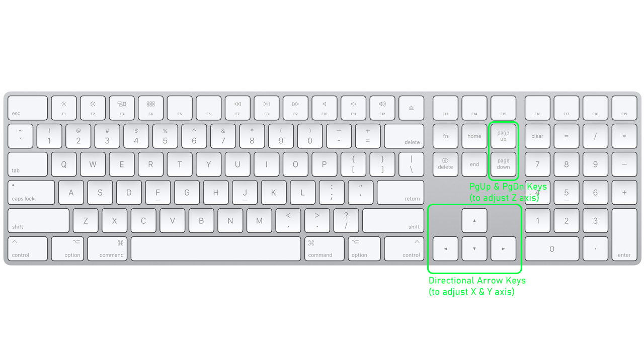
- Place the Z - Height Sensor on top of the Copper Board and do a Z - Zeroing by pressing the PgUp & PgDn buttons on the keyboard
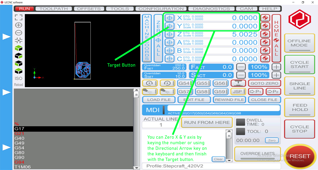
- Remove the Z - Height Sensor and do both X & Y zeroing by pressing the Directional Arrow buttons on the keyboard
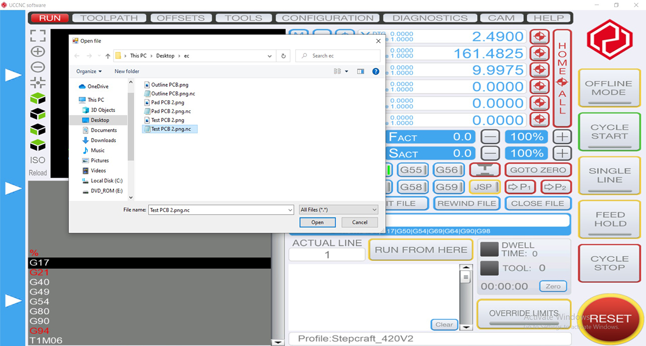
- Lastly, upload files by pressing the Upload button in StepCraft Software
- Once all setting are done, switch on the StepCraft CNC Milling Router and press the Cycle Start button
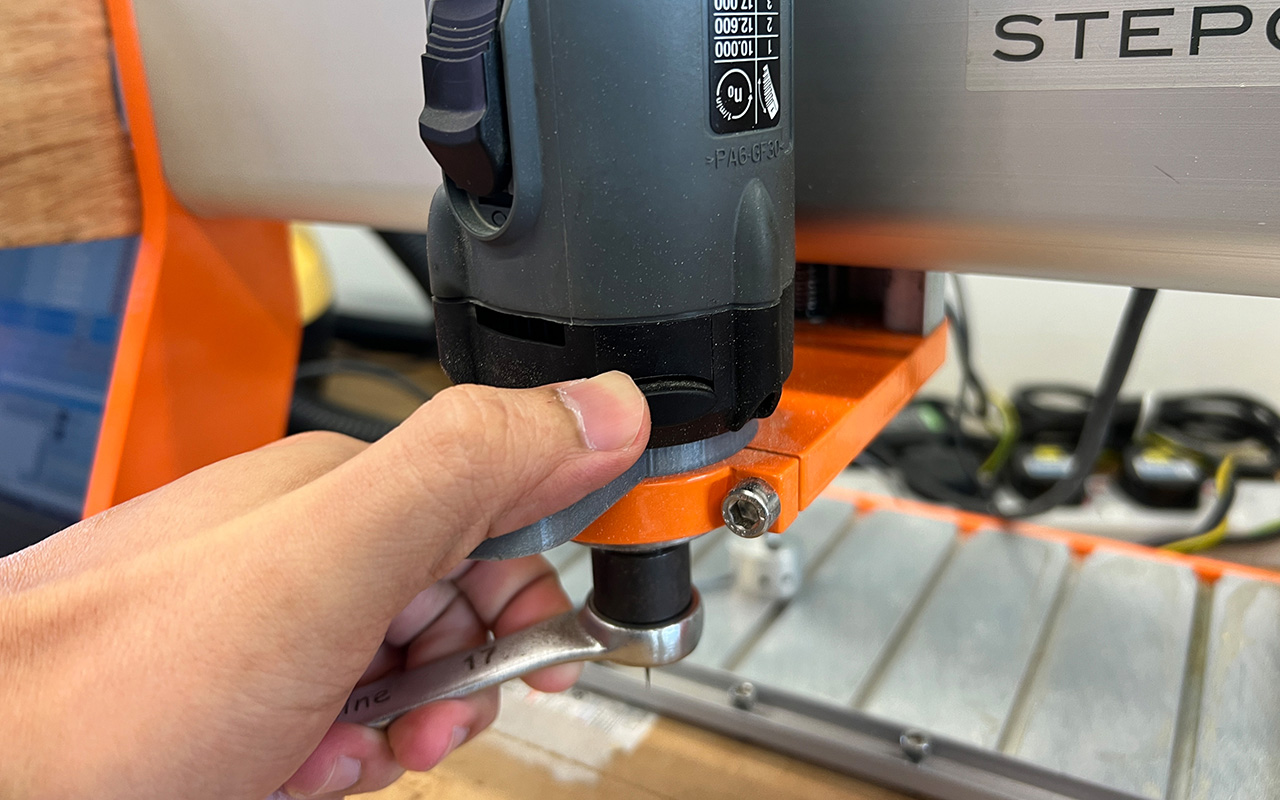
We will first need to choose the correct milling bit and fastened it to the StepCraft Router.
Next, we will prepare the Copper Board and secure it on the Material Stock using double-sided tape.
Then we will do a Z-Height Zeroing using the Sensor Probe.
After zeroing the Z-axis, we shall do the X & Y axis as well using the directional arrow keys or using the software.
Next, you may start to upload your file by pressing the Upload button.
Lastly, when all the settings are done, you may start to switch on the router and proceed with the milling.
You may also refer to the software interface to have a realtime view of the milling path and to check if the milling path is correct.
The PCB milling will start off with the Mill Traces circuit path milling then following by a Mill Outline hole milling and lastly another Mill Outline outline path milling to get the board done. In other words, we will continue with the same steps and process again. Another thing to take note is that we will need to change the milling bit to 0.8mm when we are doing the Mill Outline milling, therefore, we will remove the milling bit in the collet and replace it with the one we need which is the 0.8mm end mill bit.
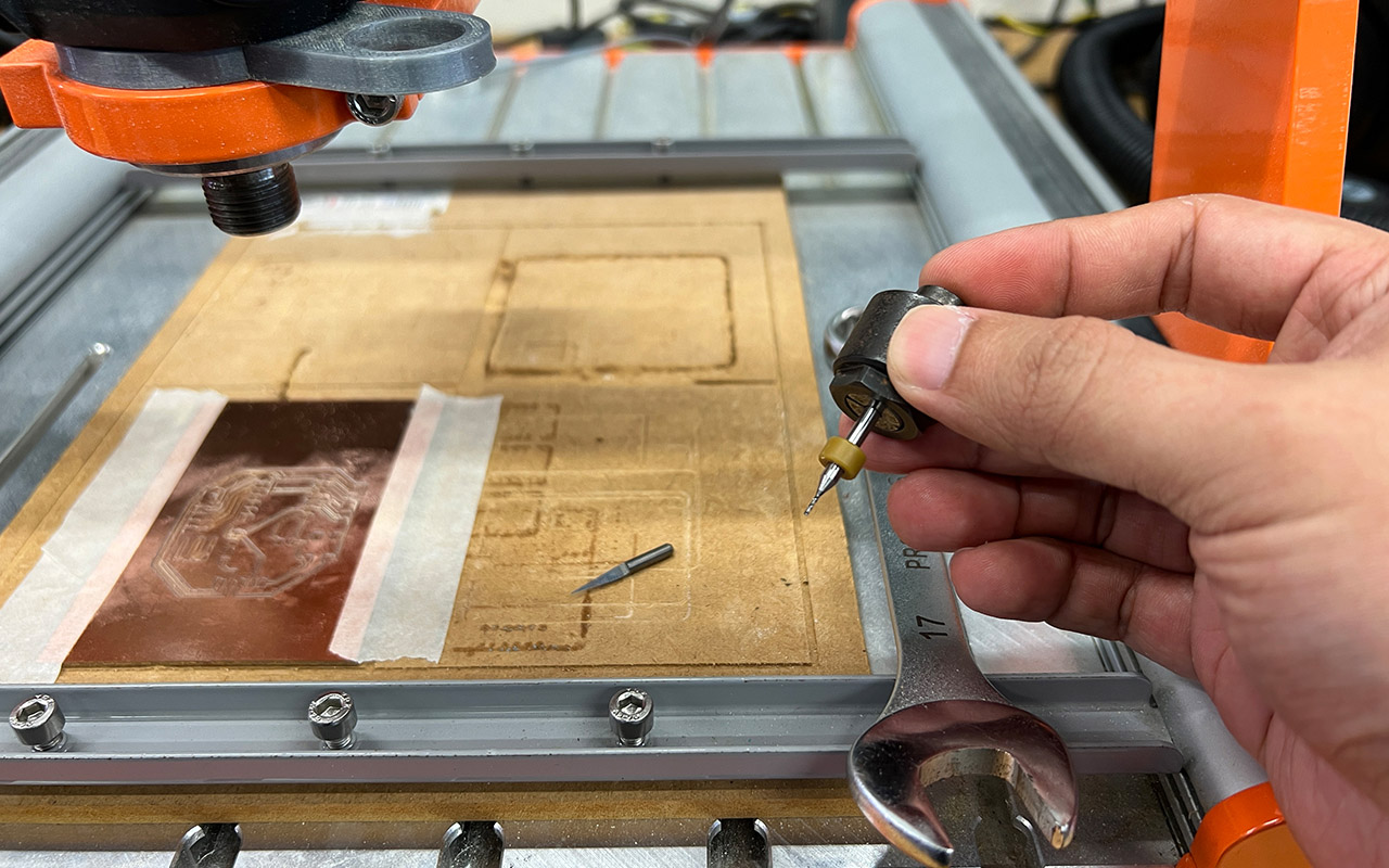
Likewise, after changing the milling bit, we will need to redo another round of Z - Height zeroing.
After Z- Height zeroing is done, we may proceed to mill the outline holes and outline profile.
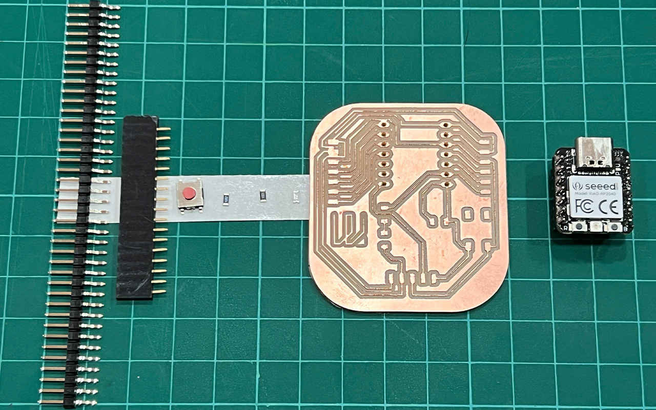
After the milling, we will use a vacuum cleaner to vacuum the debris and this should be done at every milling process before we remove the PCB from the milling bed. We may also use a pen-knife to scroll along the border of the board to allow easy removal of the board from the milling bed. Next, I will need to get the following components to prepare the soldering of my newly fabrication circuit board:
- LED
- Resistors x 2
- Press Button
- Pin Header
- Header Connector
- Seeed Xiao RP2040
Lastly, We can proceed to solder the components to the printed circuit board.
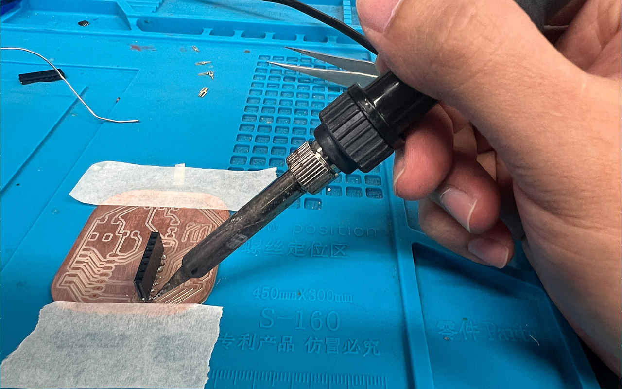
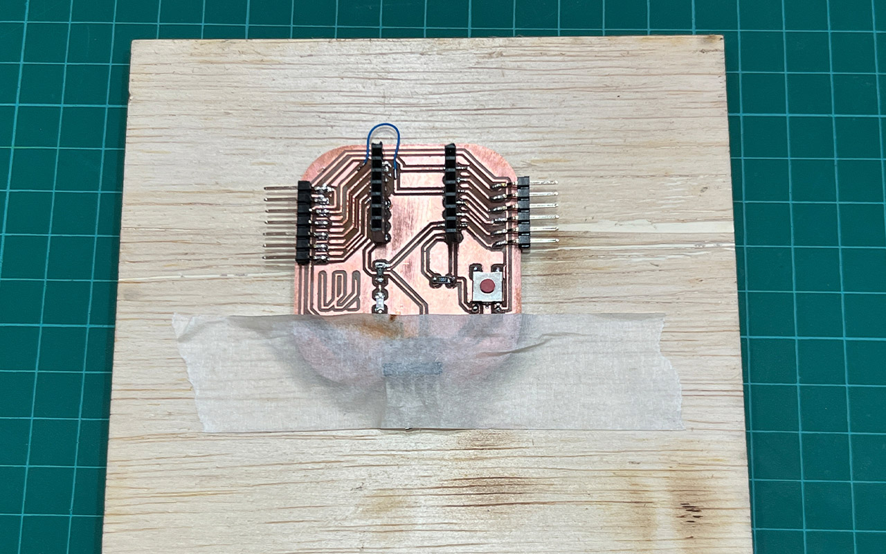
To be frank it was not easy to solder the components especially the small LED and Resistors. It took me an entire day just to get a hang of it, after a few errors and re-soldering, I manage to get my circuit board done and this is how it looks like!
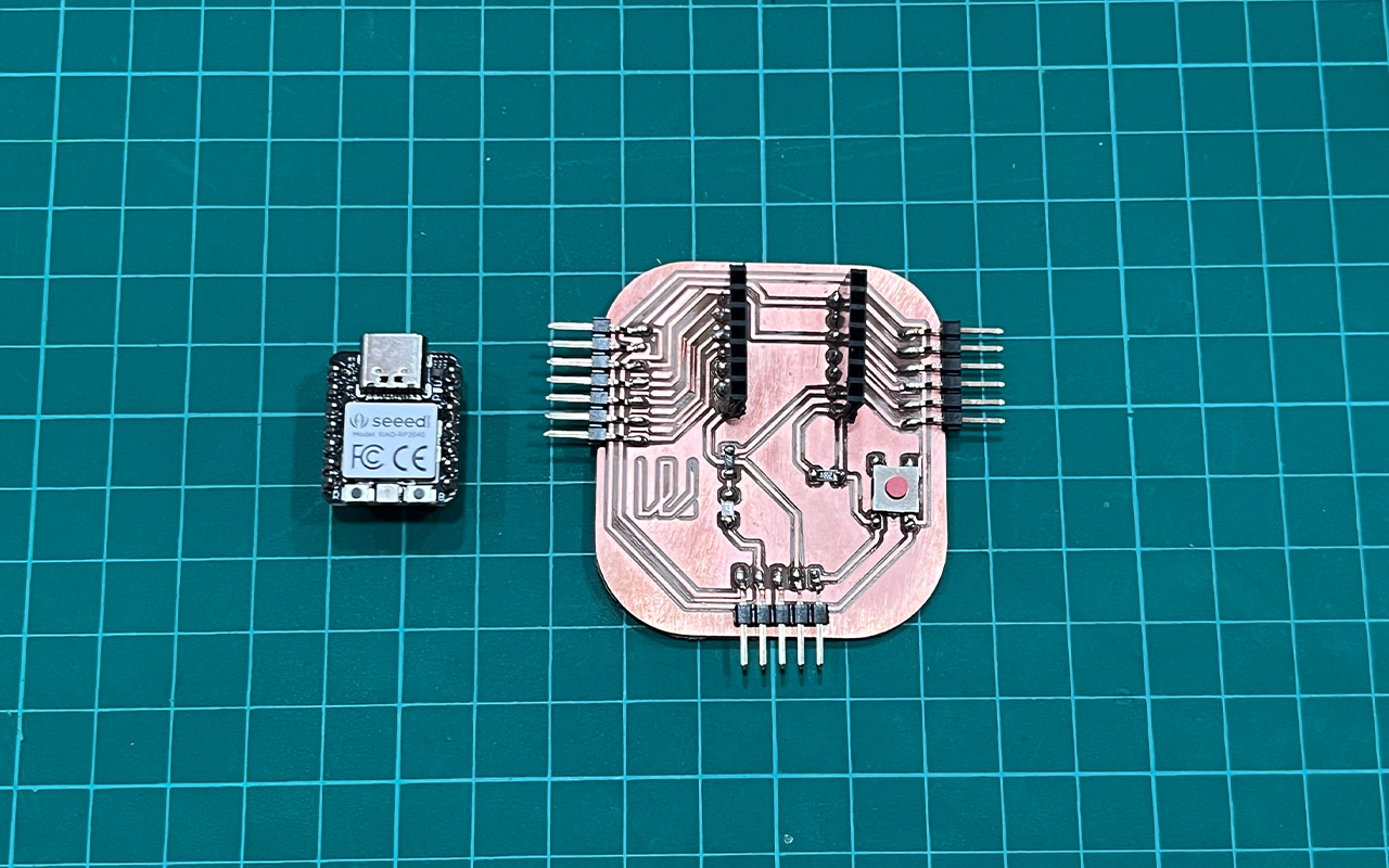
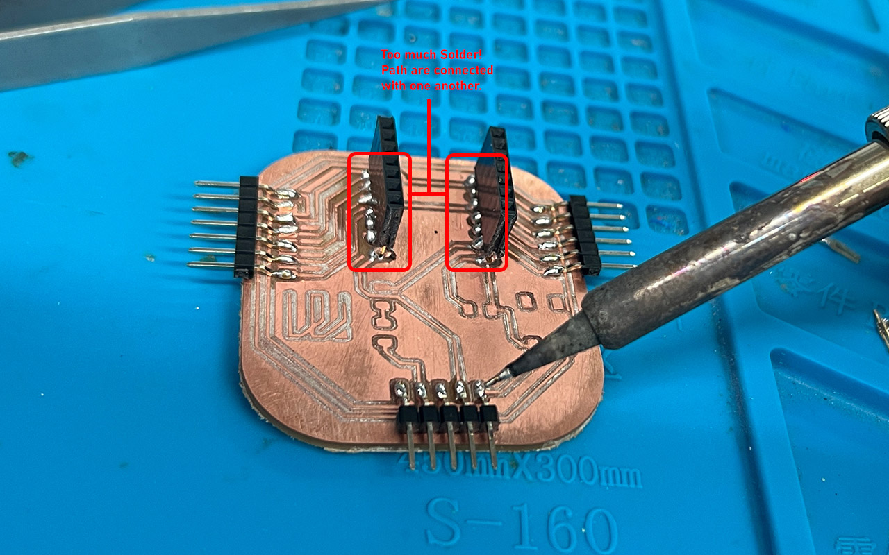
The PCB looks fine, definitely not the best but still acceptable for a first attempt. The next step is to try out the PCB and I am going to test it out using a simple digital-button programme example. However, after hooking up the board and uploaded the program through Arduino IDE, it DID NOT WORK! I am so frustrated as I had spent the entire day just to get my board fabricated and it fail! In order to salvage my board, I have tried doing a trouble shooting on my board using a Multi-Meter and test the connectivity of the paths and the soldered parts. And with the help of our local Fab Academy Instructor, we managed to detect the problems and there are many of them! Firstly I have used too much solder and some pins are in contact with one another, secondly one of my path was wrong. Lastly, my LED did not light up! (probably was short-circuit during the soldering process)
While I was thinking to myself that I had to remake another board, our Instructor said it is still possible to salvage it by doing some manual rectification to the board by soldering external wire to the rightful pin holes and path as well as using a cutter to disconnect the path. I then spent another few hours to get the all the issue rectified, from cutting & disconnecting the path that was wrongly connected (this resulted to my Resistor that was connected to the switch to be redundant and I had to use an Internal INPUT_PULLDOWN for my button Pin), unsolder and re-solder a new LED etc. and this is how it looks like after 2 hours of electronic surgery:
The next step will be a test of faith, to check if my PCB works. I then upload a simple Button programme to test the board. I link up the button Pin to D7 pin and LED to D8 Pin of the Seeed Xiao RP2040 board.
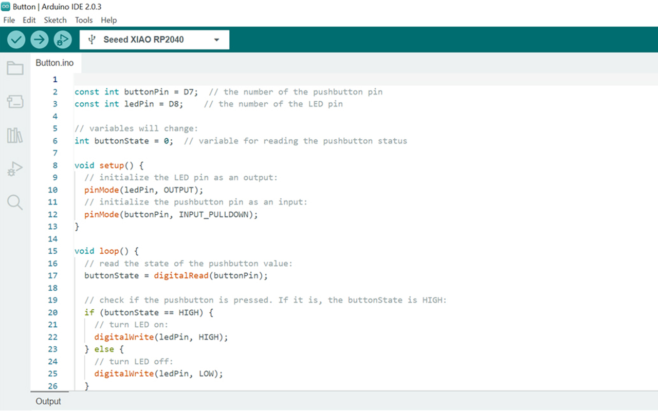
And my PCB finally WORKS! It flashes when the button was pressed which is what the program code should do.
Reflection
It was really a long and tedious week of electronics production / fabrication as along the way, I have made many mistake from saving & preparing the wrong file, to not even switching on the router during cutting which causes one of the milling bit to have a broken tip etc, not to mention that I was away for 3 working days to attend a course which reduces the available time that I have to do my assignment. Nonetheless, I still manage to fabricate my first PCB and that in a way give me a sense of acheivement as I now know how to actually design and fabricate my own PCB.