6. Electronics Design
This week I started to work on Electronics Design that includes learning how to use a Regulated Power Supply, Multimeter and Oscilloscope. I have also learnt on how to design my first Printed Circuit Board using Autodesk Fusion 360/Eagle Electronic Design Software. The group assignement is to learn how to use the Regulated Power Supply, Multimeter and Oscilloscope to check for voltage and current values as well as how to read waveforms. Our group members have work together on testing these equipment and also learnt on how to read the information with the guidance of our local Instructor.
You can access the group assignment HERE.
Electronic Printed Circuit Board - Autodesk Fusion 360/Eagle
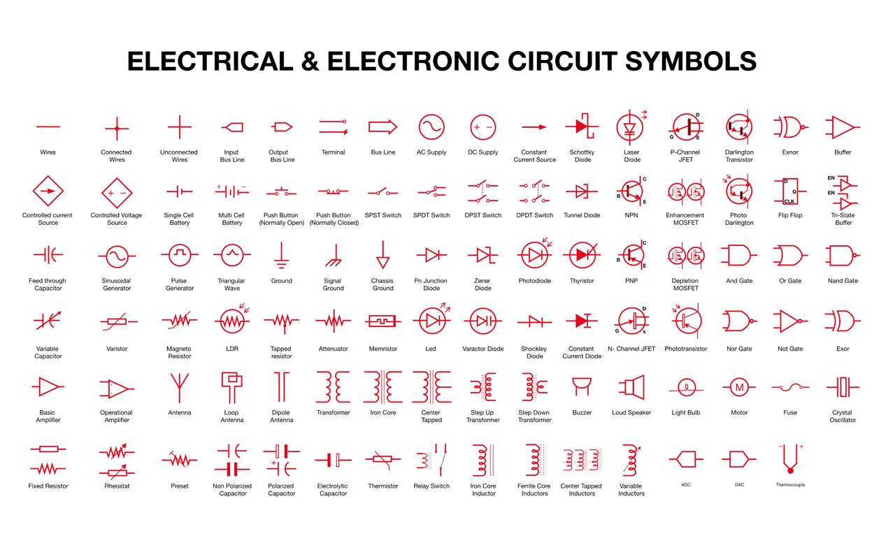
For this week assignment, I am going to learn and create my first printed circuit board (PCB) through Autodesk Fusion 360/Eagle. Before I start to create the circult design, I will first need to learn how to read and understand the schematic circult drawing and its electronics symbols. As I am do not have a background on electronics/electrical, it really took me quite a while to understand and memorize what does each symbol represent.
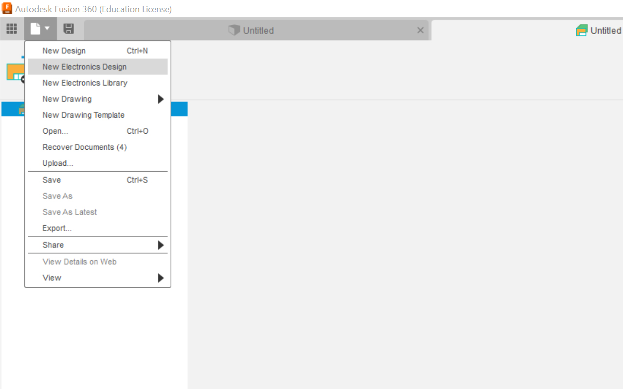
So to begin with the circuit board design, I will first need to download the library of electronics symbols so that I can use them for my assignment and project. I then launch Autodesk Fusion 360 and look for New Electronic Design under the UI tab.
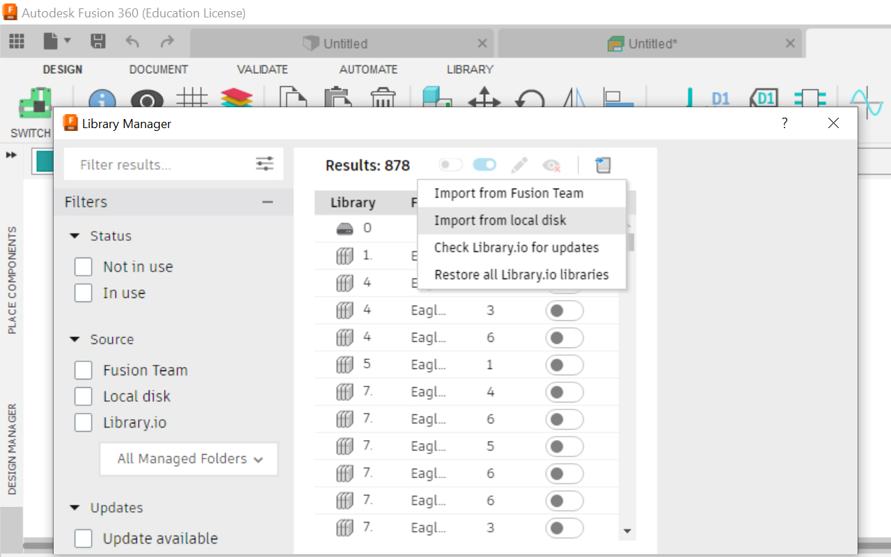
After launching the software and selecting the new electronics design function, you should see a new interface as shown in the image below and the next step is to select the Place Component tab on the left hand side and look for a small icon on the top right hand corner to open the Library Manager. While inside the library manager, you can select the file (which I have downloaded earlier from Fab Academy into my local drive) and install it afterwhich you will be able to access all the components and use them under the Place Component tab by double clicking on the component.
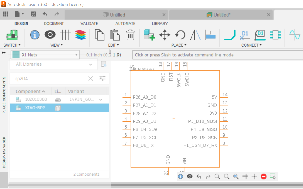
As I am going to use the Seeed Xiao RP2040 micro-controller, I will just need to key in RP2040 in the Filter Box and the relevant component will appear below in the component box. I will then double click on the component that I want and place it on the working interface beside it. But before placing, I need to know what are the components I need to create the PCB board for my micro-controller so I have to seek advise from my local instructor and then listed down the following components that are required:
- 1x Seeed Xiao Rp2040 Micro-Controller
- 1x LED
- 2x Resistor (1kΩ & 10kΩ)
- 3x Pin Header
- 1x Button Switch
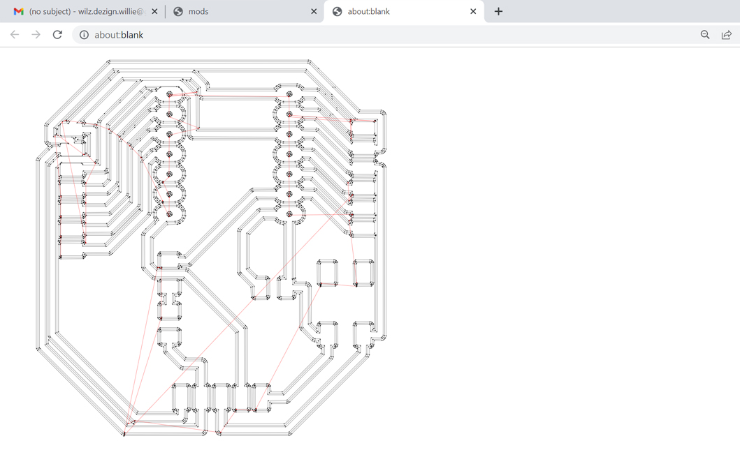
It took me some time to familiarise with the software and playing around with the components but with the guidance of our local instructor, I have eventually manage to create the schematic drawing circuit of my PCB design after many many tries.
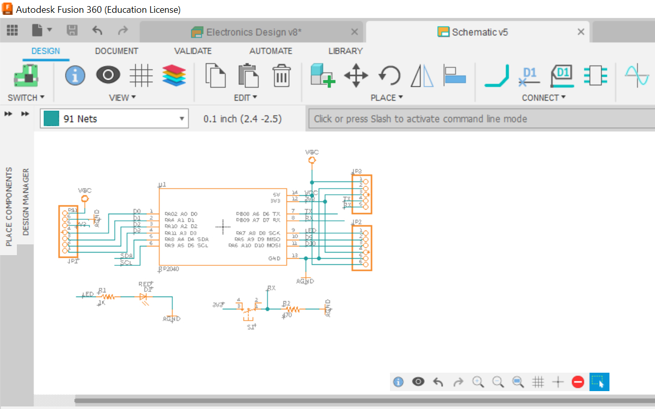
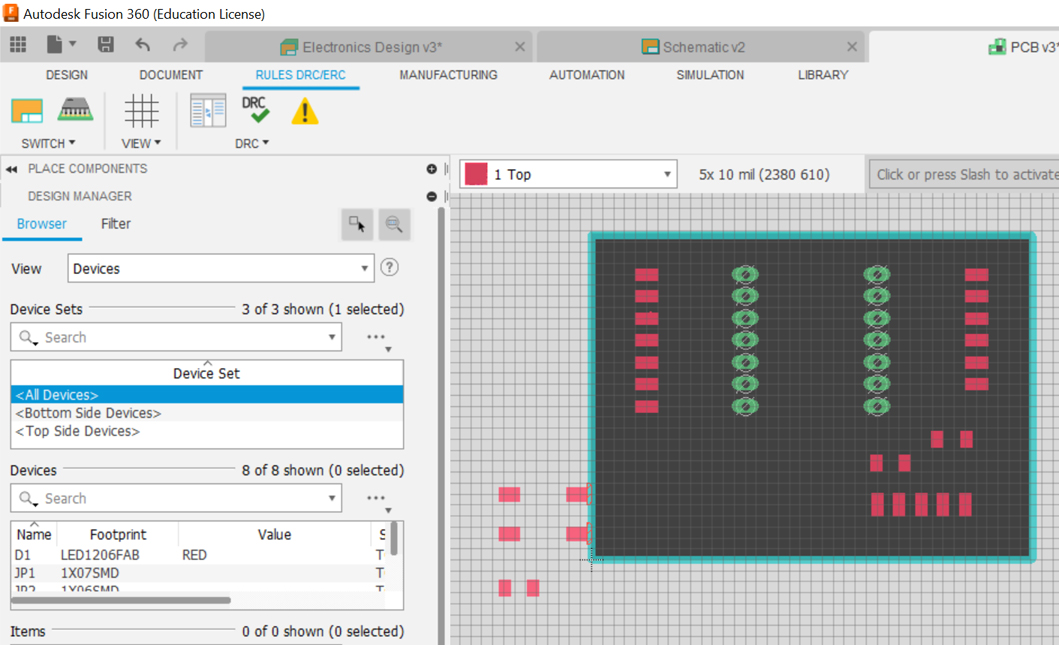
The next step is to switch the working interface into PCB document (under the Switch tab) whereby I will need to manually adjust, place and link up the all the components together. This is acutally the most time consuming part of the entire circuit board design as there are alot of trial and error that requires us to try and then amend the schematic drawing so that we can acheive the most ideal linkage route to all the component which then makes it possible to be send for CNC milling production.
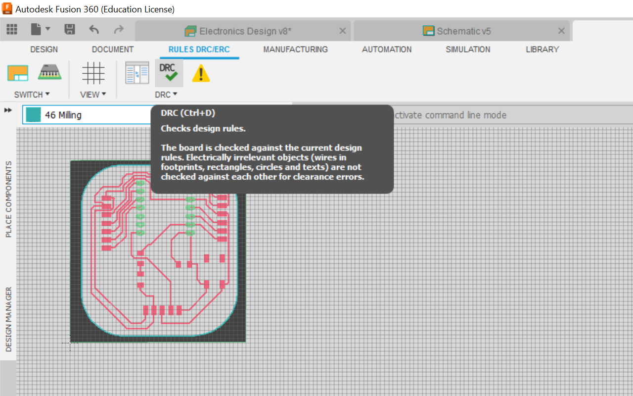
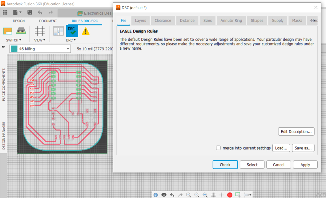
After the placement of the components are done, the next step is to check the circuit if they are correct and in order to do that, I will need to creat a Checklist of Design Rules for the circuit board design. I can create the design rule by selecting the DRC icon under the Rules DRC/ERC tab. Once I have key in the parameters (such as the Clearance & Distance checks), I can press the Check Button to see if my circuit design is correct. If nothing appears i.e there is no Error box, that would mean that the circuit design is good for production.
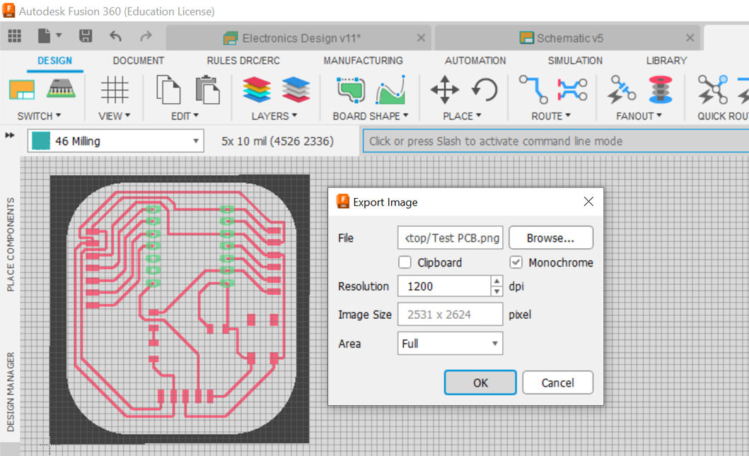
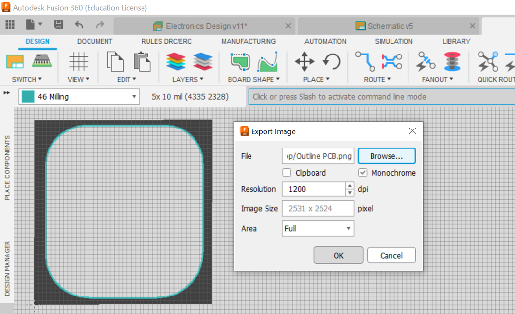
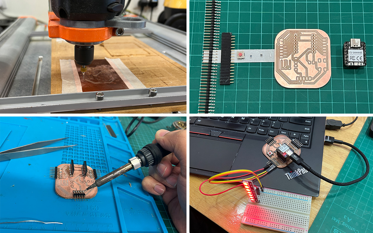
Lastly, I can just type Export under the Command Line Mode to create an image of the PCB for CNC milling. I will need to change the resolution to at least 1000dpi (in my case, I change the resolution to 1200 dpi instead) and select Monochrome for the exporting of image file that is to be use for CNC milling. Before exporting, I will need to ensure that I am exporting only the layers that is required and in order to do that, I can just hide or unhide the specific layers under the Layers tab. Last but not least, I will need to export 3 images for the production of my PCB design as one image is for the circuit routing milling, one image is for the cut-out of the PCB and the last image is for the holes. In the case of my board design, I have made it into a square shape design with round fillet corners.
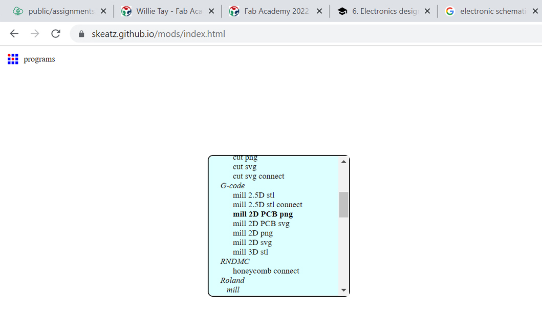
After exporting the images, I will need to use the MOD program (Mill 2D PCB PNG) so that I can generate the G-Code for my PCB design production.
The next step was relatively easy as what I need to do is to upload the image and select the parameter settings to CNC mill the PCB design.
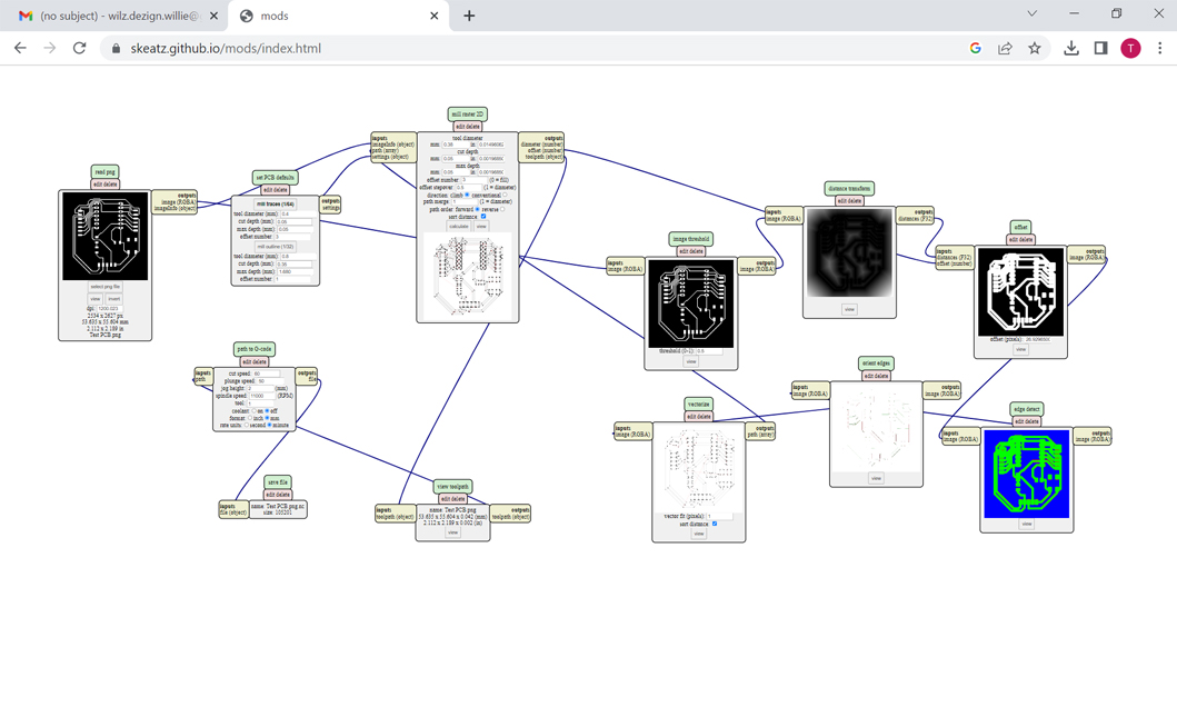
Last but not least, after I have adjust the parameter settings for the CNC milling of my PCB design, the very last step is to press the Calculate Button and the G-Code will be generated for you as shown in the image below:
You may download the 2D PCB PNG file HERE.
Below is the hero image of my PCB design & fabrication processes which I have done during the electronic production week.
Reflection
So far so good for the electronics design exercises but it was quite a long week for me as I need to read up on some fundalmentals on electronic design and to play around with the circuit design as well. Coming from a non-engineering background is really tough and trying to understand all about electronics design within a week is really really HARD! But nonetheless, it was a good experience as I have learnt something very useful as well as new skill which allows me to do PCB design and production.