Week 6: Electronics Design
Assignments
The assigments for this week are:Group Assignment
Use the test equipment in your lab to observe the operation of a microcontroller circuit board
Individual Assignment
Design a development board to interact and communicate with an embedded microcontroller
Group Assignment
For the group assignment, we were to test the equipment in our lab to observe the operation of a microcontroller circuit board. In our case, the equipment we tested were the multimeter, the oscilloscope and the power supply. The microcontroller circuit board we tested were the Arduino Uno and the Xiao RP2040. What I learned from this assignment is that the equipment are very useful in testing and prototyping of the circuit board. The multimeter is handy in troubleshooting the circuit board by measuring the voltage, current and resistance. The oscilloscope allows us to observe the signals, while the power supply is able to provide the desired power to the circuit board. Full documentation can be found in the Group Assignment Page.Design a Development Board to Interact and Communicate with an Embedded Microcontroller
Designing the Board
For this individual assignment, Autodesk Eagle were used to design the development board. Autodesk Eagle is integrated with Fusion 360. Since we are already using Fusion 360 for our CAD, it will be convenient for us to use Eagle. To begin, we first need to import the two libraries into Eagle: one is the Fab Academy library and the other is the library for XIAO RP2040. To import the libraries, we had to launch Fusion 360 and then open a New Electronics Design under File.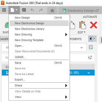 Then, Select New Schematic and import the libraries from there.
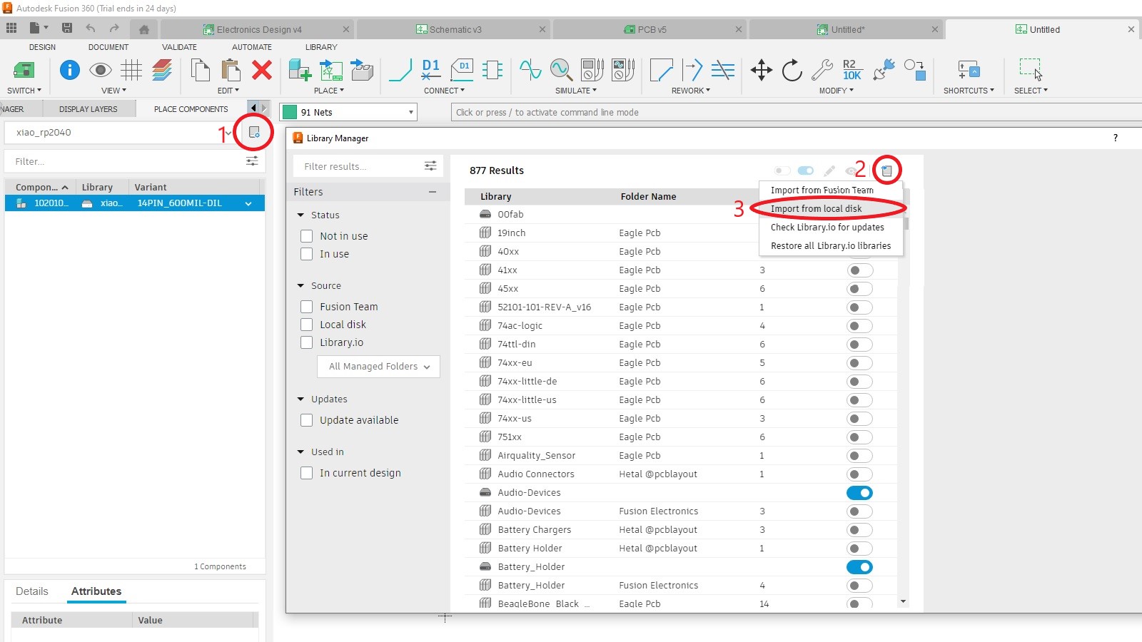 After the libraries were imported, the components required can then be selected and placed on the workspace. Then the components were positioned and linked to the MCU using the shortcut key R.
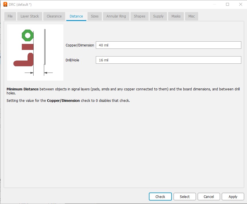
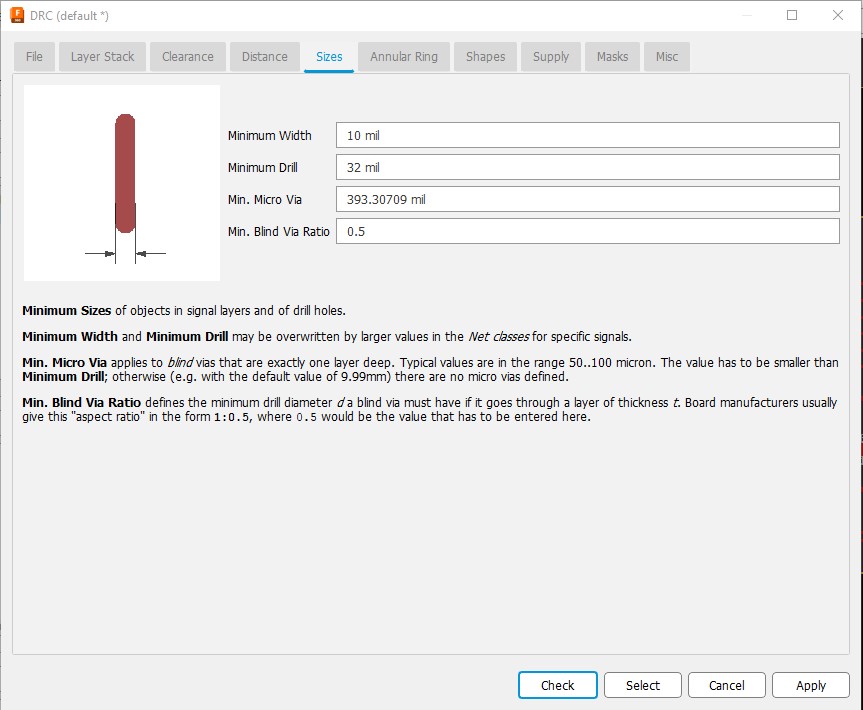
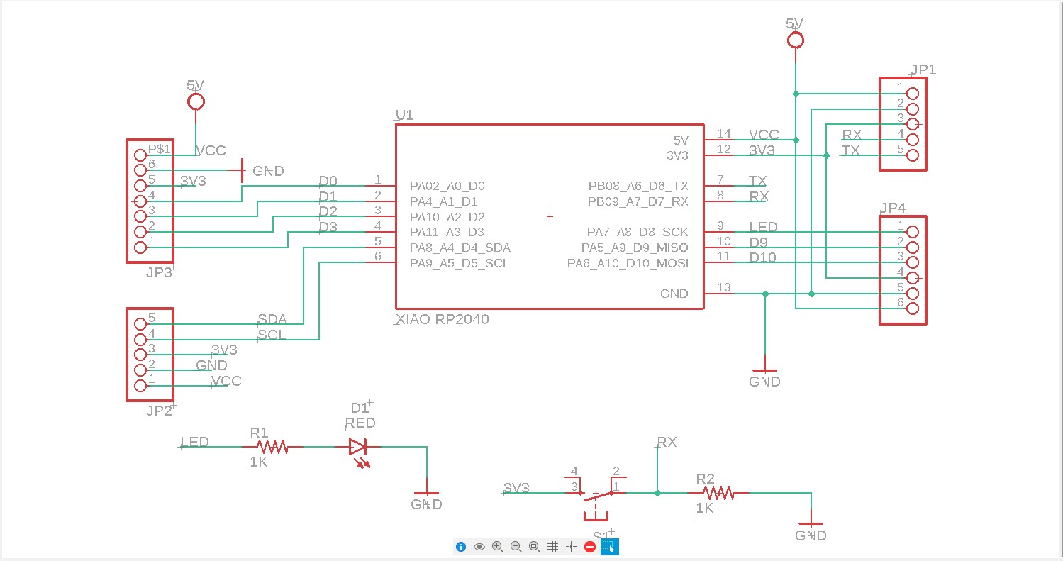 When the schematics were done, we switched to PCB document. Here the components were laid out again. The DRC settings were adjusted.
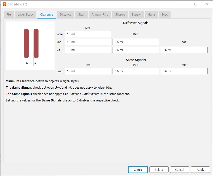
 The circuit paths were then routed. This is the most time consuming part of the process. After the routing was done, DRC was run to check for errors. After all the errors were corrected, the circuit design was ready for export.
Exporting the Design
I will be exporting the circuit design for milling with LPKF E34 PCB milling machine. Before starting to export the design, I went to Preference>Electronics and untick the "Display signal names on pads" amd "Display signal names on traces" options.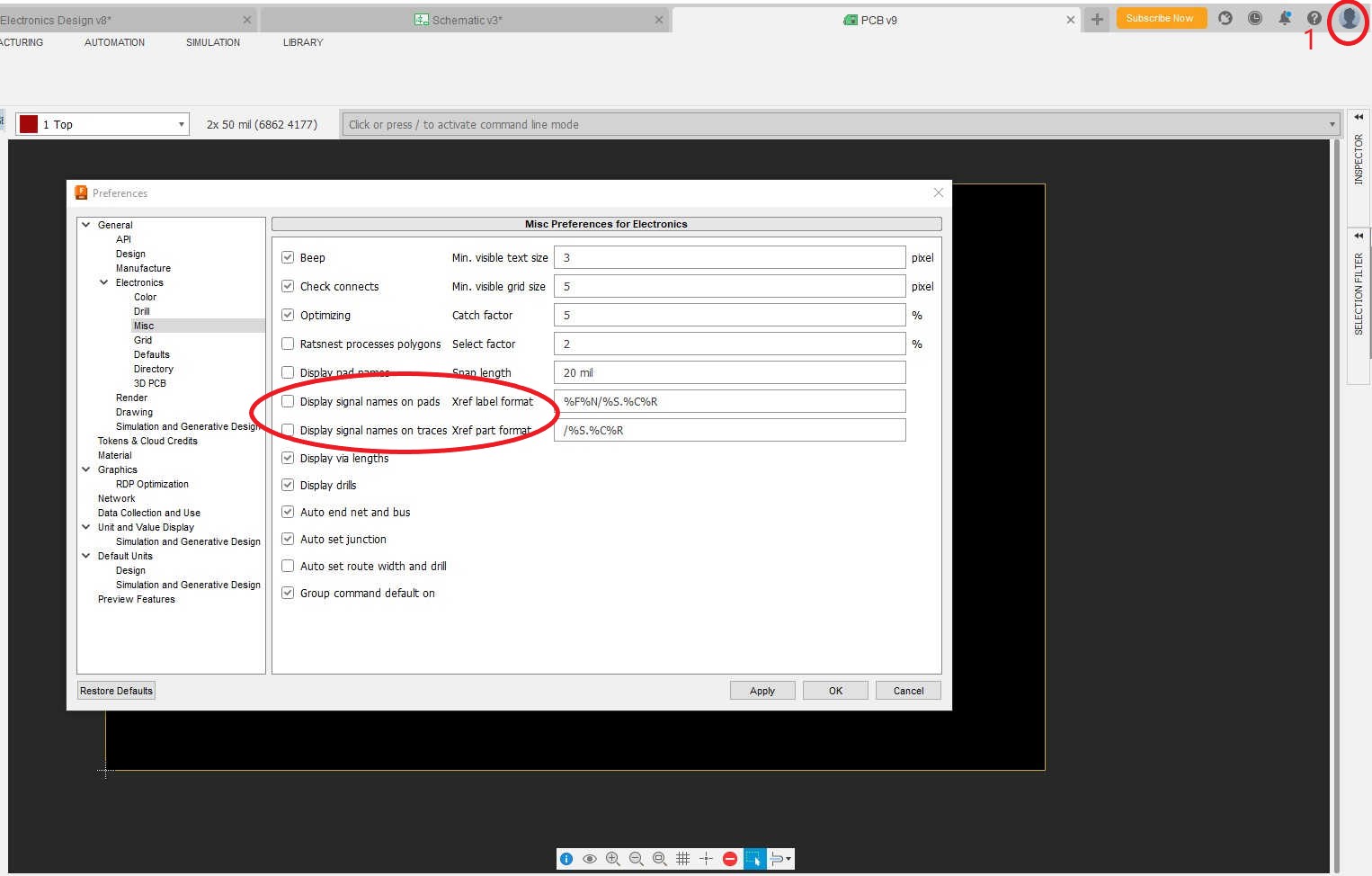 After setting the preferences, all the layers are hidden excpet layer 1, layer 16, layer 17 and layer 20.
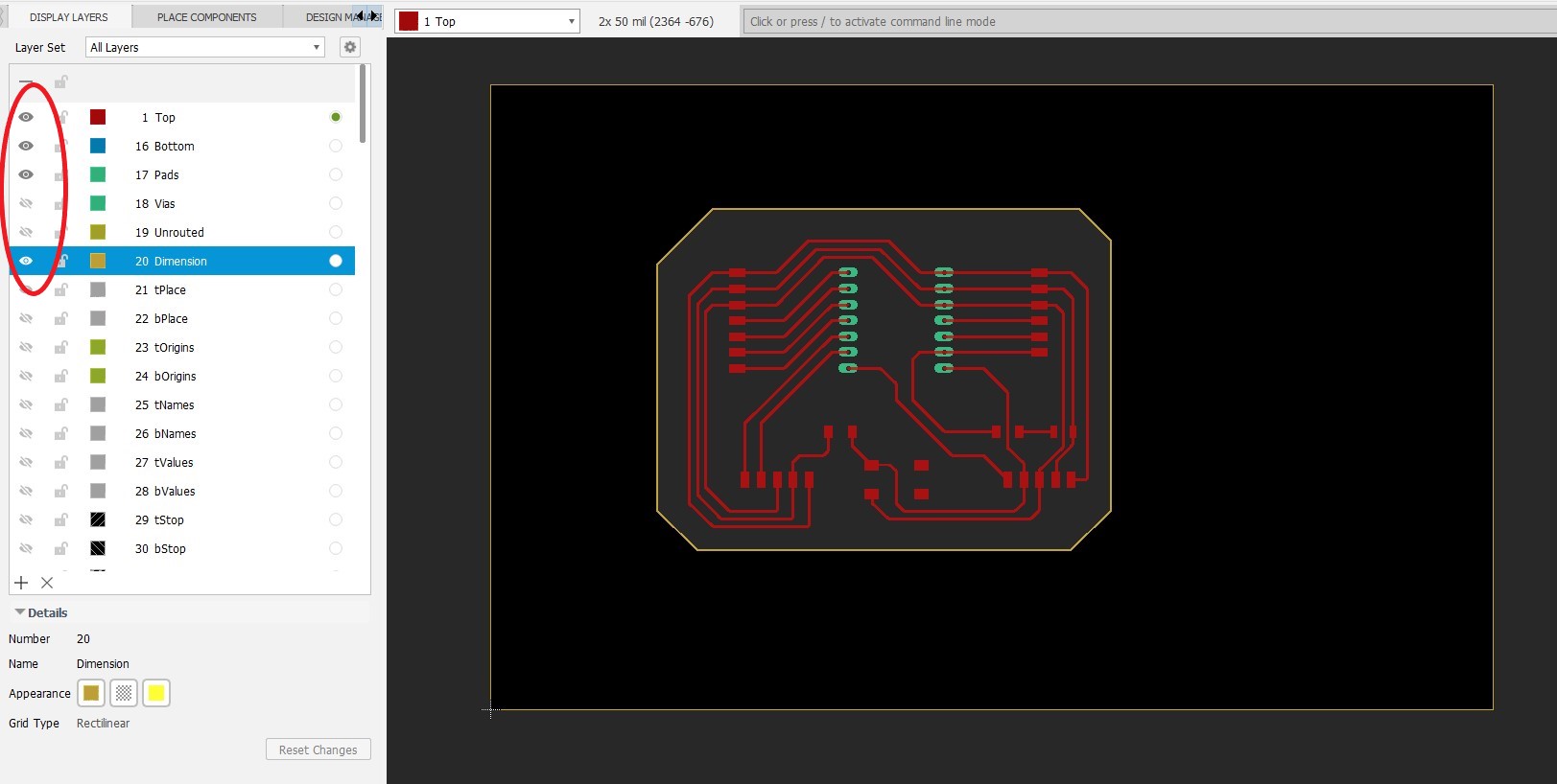 Finally, the circuit is exported as a png image by typing "export image" in the command bar. The export image dialog box will appear after the command was keyed in. The resolution was set to 1500 and the design was exported.
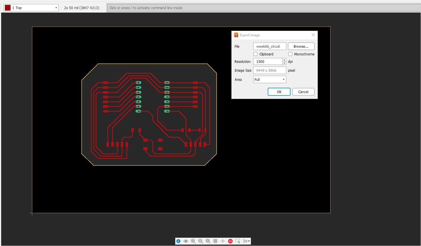 The exported PNG was further processed in Inkscape with the trace bitmap feature to generate a vector file. The vector file was then saved as a DXF file, which will be used for milling the circuit.
Design File
Fusion 360 file for the PCB design.PNG file of the circuit design.
DXF file of the circuit design.