dummy
6. ELECTRONICS DESIGN
On Week 4, "Embedded programming", we learned how to use simple codes with the XIAO RP2040 Microcontroller, but to do so we used a "Bread Board to make the cabling connections between the components and the Microcontroller Pins.
This week we got to design our "personalized Board" it is hands on software and hardware to design it. Instead of having the breadboard to do the connections, we designed the board making the connections directly into a board as it would be in a final product design, the Breadboard is a semi-permanent prototype of electronics circuits.
HERO IMAGE
ASSIGNMENTS
Group Assignment
- Use the test equipment in our lab to observe the operation of a microcontroller circuit board.
Individual Assignment
- Design a development board to interact and communicate with an embedded microcontroller.
- Extra credit: try another design workflow.
- Extra credit: make a case for it.
- Extra credit: simulate its operation.
GROUP ASSIGNMENT
For this assignment we met with my fellow students and Steven our instructor, he guided us through the different equipment we have in the Fab Lab to test boards and Microcontrollers.
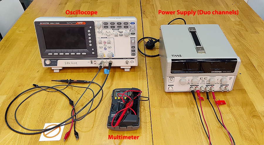
I found particullarly interesting the Oscilloscope, it is an equipment that can give so much information not only from the hardware but from the coding itself. We did a comparison between the Arduino Uno and the XIAO RP4020 with the same coding of Blinking a Led Light, then we measure their waives and we could see the difference on the waives height as the Arduino Uno microcontroller was connected to a 5v ant the XIAO to 3v. We could see too the accuracy of the time in both waives, given the delay of 500 ms between ON-OFF in the loop.
Then we took out the delay from the coding and could see the speed of the internal clock, in both cases both were a bit behind trying to complete the loop the waive. Steven tought us that we can do "Bare Metal Programming", in the Data sheet of the microcontroller and its components, we can learn how to code to go directly to the internal clock to make the loop faster, changing the time difference from miliseconds to nanoseconds.
You can see HERE more about the group assigment, where we see more in detail the different 3D printing properties.
INDIVIDUAL ASSIGNMENT
-Design a development board
This board should interact and comunicate with an embedded microcontroler.
I have decided to use the integrated software AUTODESK EAGLE for designing my board.
The main objective of this board is to expose all the pins of the Microcontroller for external use, making them readily available for connecting with external components. Additionally, I want to include two built-in components, a switch and a LED light, that can communicate with each other.
To start I had to go to the FAB ACADEMY LIBRARY to download the Eagle Library, where are a lot of the components used in electronics design.
To add the necessary components for the board to the schematic document within the program, we can use from the library and upload it:
- XIAO RP4020 Microcontroller
- Pin Buttons, two of 5 and two of 6
- A switch button and a resistor
- A led light and a resistor
- Symbols as Ground and 5V,
When I have all the parts in the Schematic Document I started to trace the paths or connectios between the components, assigning each of the Microcontroller pins to the extension pin. Each of the Pin Buttons has, one ground, one 3V, and one 5V the other are left for the data points. In this way I have all the pins available to connect different components to the Board.
The Led and the pin Button are built in the board, and are connected to the Pin Buttons. each of them requires a resistor to calibrate the voltage.
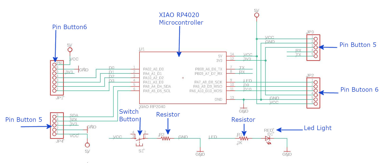
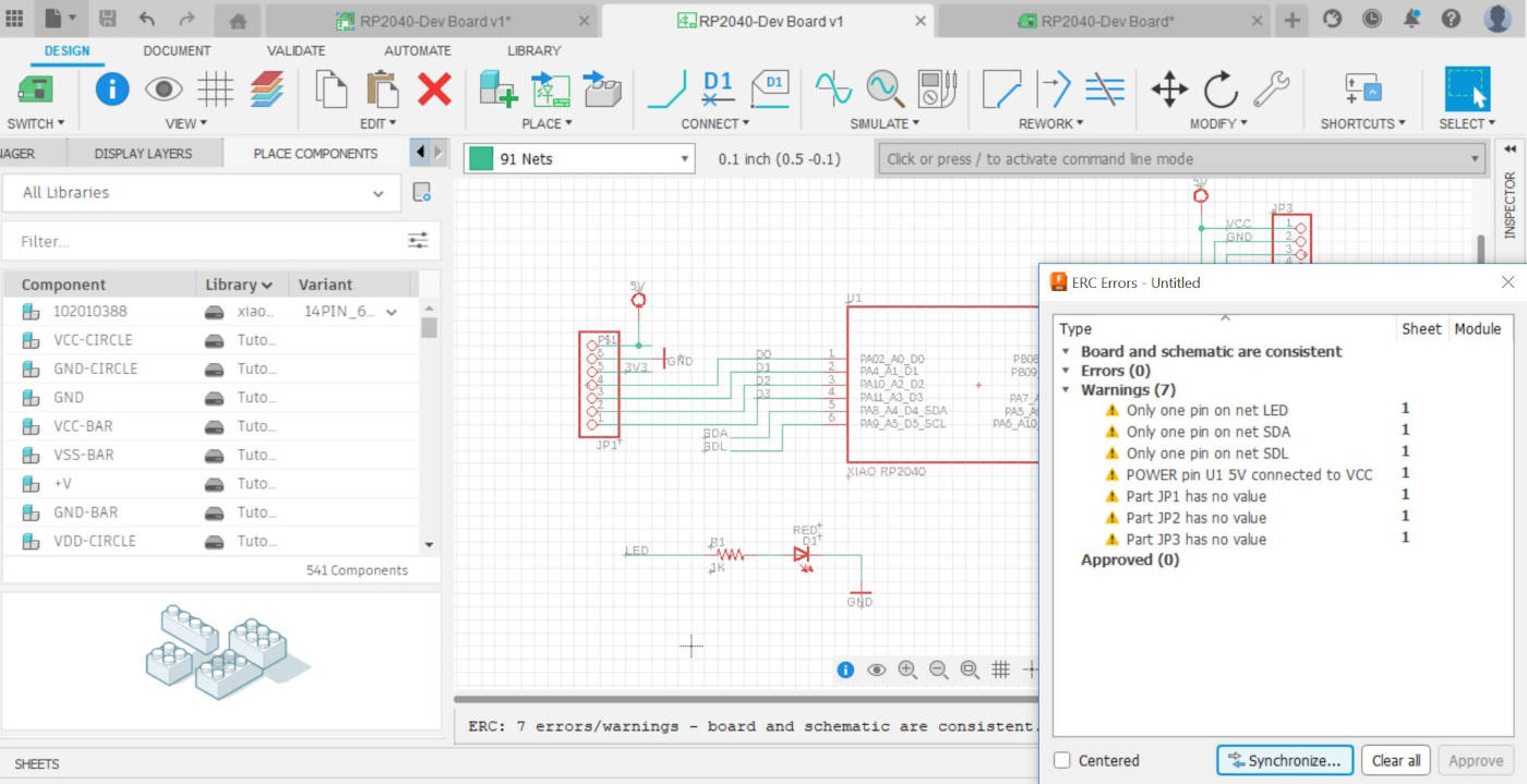
Before moving on to the PCB format, I ran the ERC (electrical rule check) controller to check for any discrepancies in my schematic design. This is a good practice as it can help avoid potential issues later on. During the check, I found some errors which I fixed, but I also noticed some "errors" that were actually intentional, such as the value of some pins that were not needed, like the Power Pin connected to VCC. This was done intentionally to provide flexibility in the set of pins, allowing them to be connected to either 3V or 5V depending on the specific requirements.
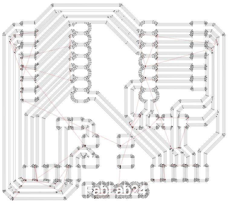
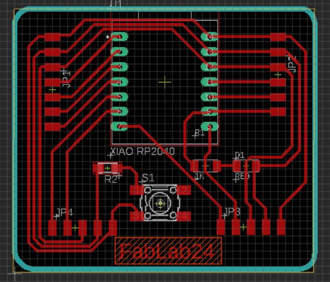
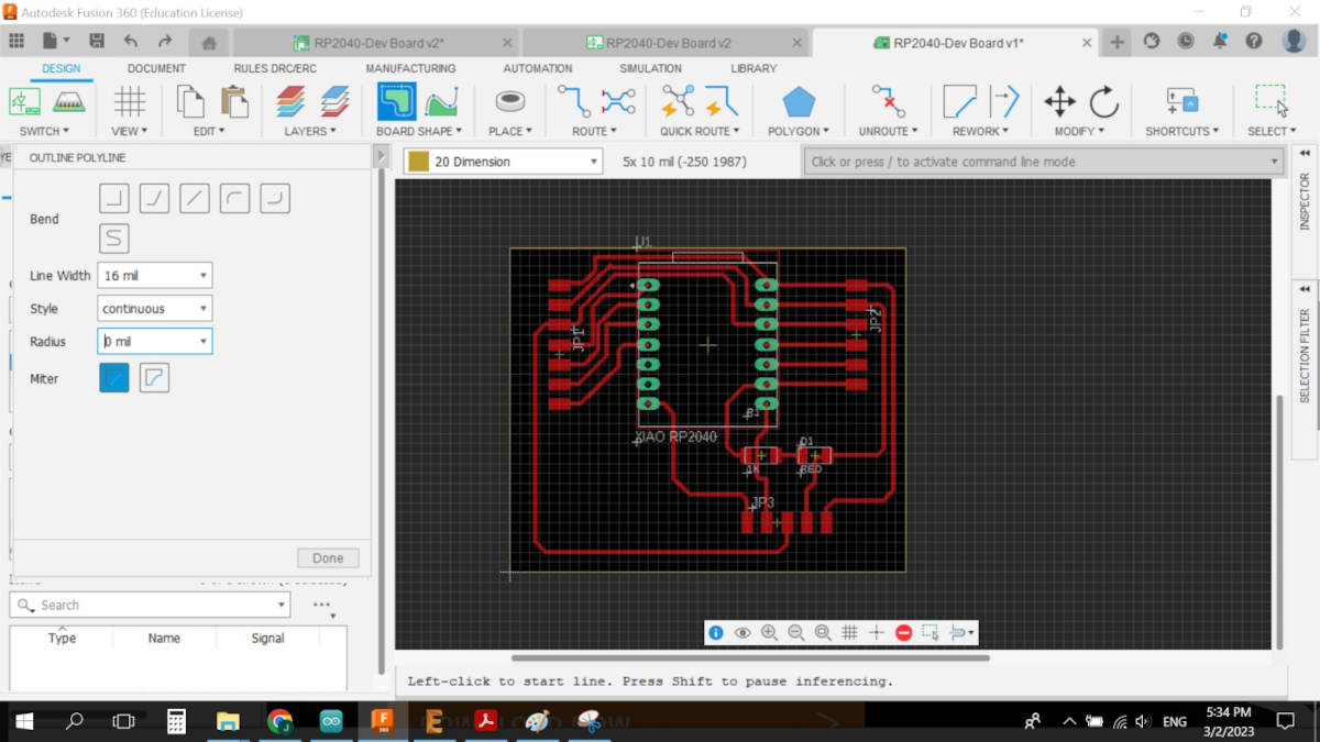
After completing the schematic diagram check, I switched to the PCB document in the program. Here, all the components and paths between them were automatically "sent" to a board setting, but they were initially disorganized. I had to manually move each of the components to their final placement, making sure to leave enough space for the paths that I would later print with the CNC.
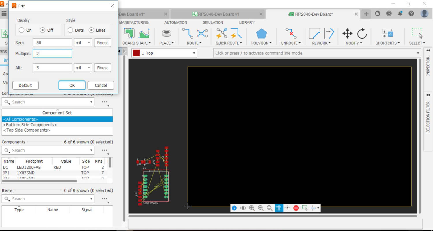
Before starting to move the components around, I adjusted the grid size to help guide me with the movements and traced a working area starting from the 0,0,0 origin point
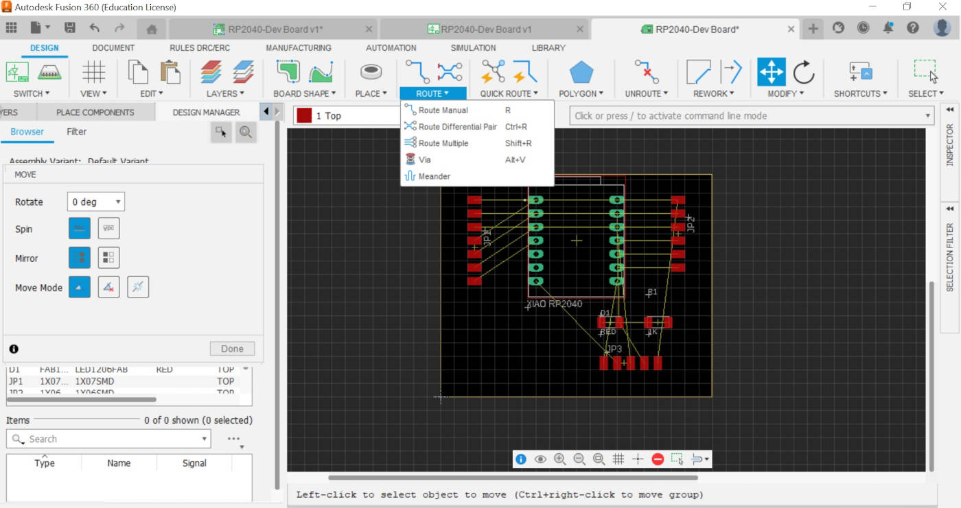
Once I had positioned the components approximately where I wanted them, I started tracing the paths that would connect the different pins. I went to the Route tools and selected manual mode, which allowed me to have better control over the paths.
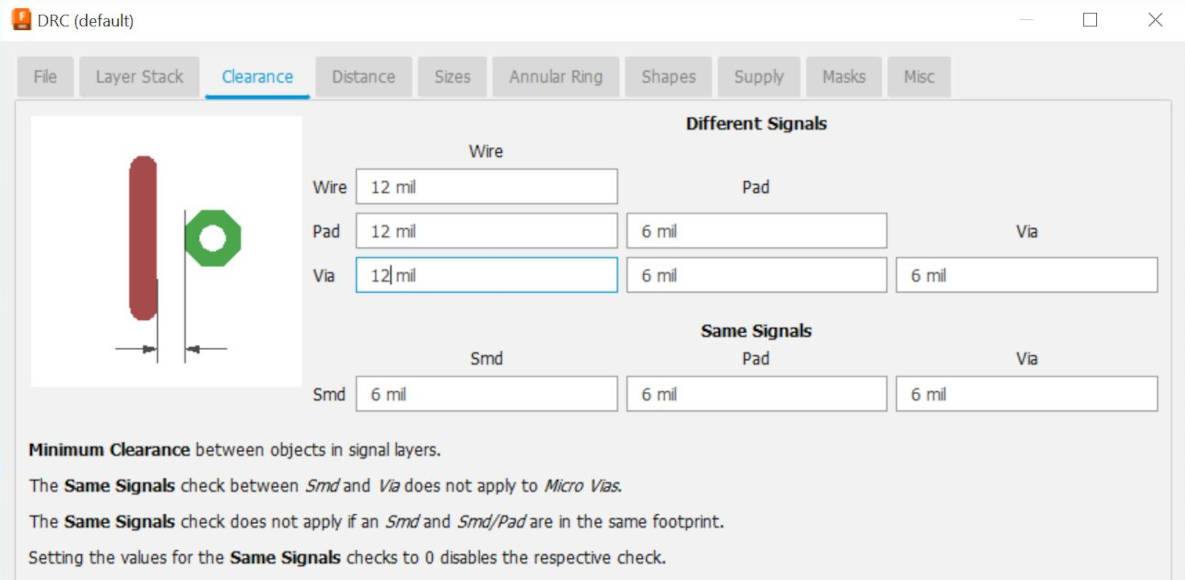
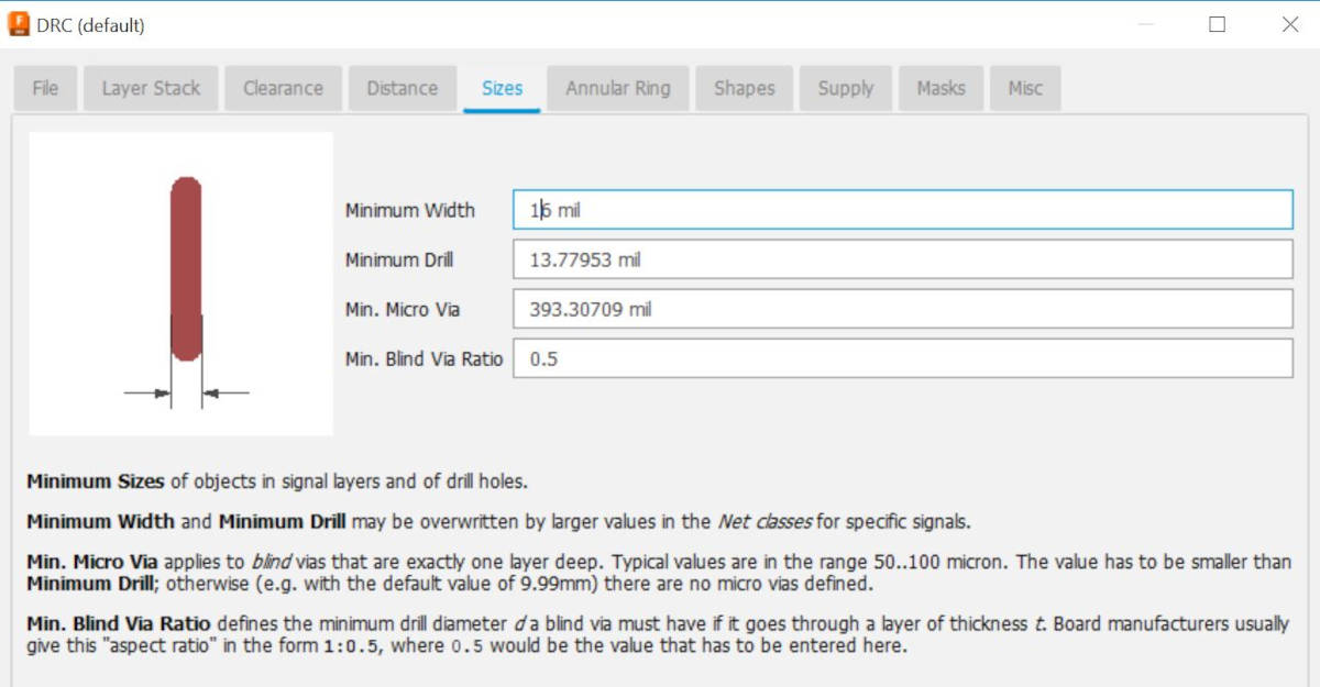
When I was working on the PCB design, I made sure to go to the DRC (Design Rule Check) settings and adjust the sizes to ensure a good space between the paths and the size of the paths. I set the spacing between 12ml and 16ml, which worked well for both. This step is very important, as it prevents the paths from getting too close to each other and generating errors when trying to get the template for the CNC in Mods.
After I finished preparing the pads, I proceeded to draw the outer line of the board by going to the Manufacturing tools and selecting "Outline polyline". This allowed me to create the final shape of the board, which I could then use to generate the necessary files for the CNC machine.
At this point, I was able to go back to the schematic and add more components or change connections between them if needed. I made some additions and changes in the schematic diagram and then ran the ERC to rule out any errors. Next, I traced the new paths in the PCB document and ran the DRC to check for errors. I discovered that most of my errors were due to bad connections to the center of the pins, pads being too close to each other, and broken paths. Fortunately, the DRC showed me where the problems were and what needed to be fixed.
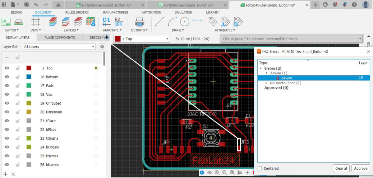
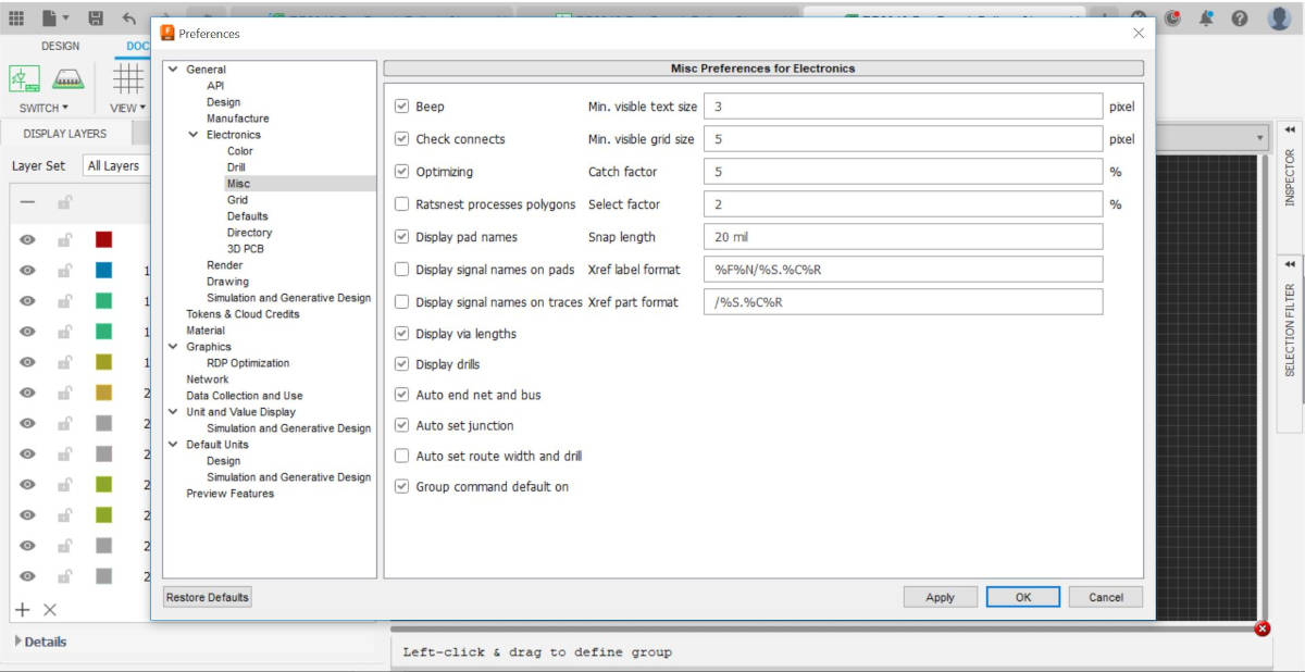
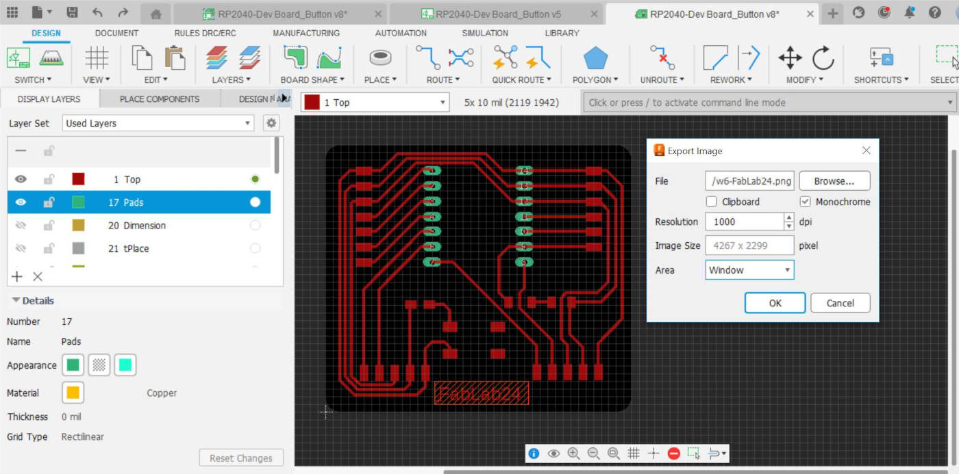
I was able to move the paths around once they were already traced, and I spent some time organizing them and giving them more space between each other. It was important to carefully check the board for errors and fix them to ensure that the routing and drilling would be accurate. Once I had checked everything again and all the DRC errors were cleared, I exported the image to PNG. Before doing so, I made sure to go to Preferences > Electronics and untick the "Display signal names on pads and traces" option, and then clicked OK.
I exported the image by typing in the command prompt, and a window appeared where I selected the location to save the PNG. I chose to make it monochrome and set the resolution between 1000 and 2000. I selected the area as file, not window. I exported two images, one for engraving the paths and another for cutting through the board. In the layers section,
I only kept layer 1 Top where I drew the paths and added text. I also kept the layer of the Microcontroller pads, as these areas would be left without engraving by the CNC.
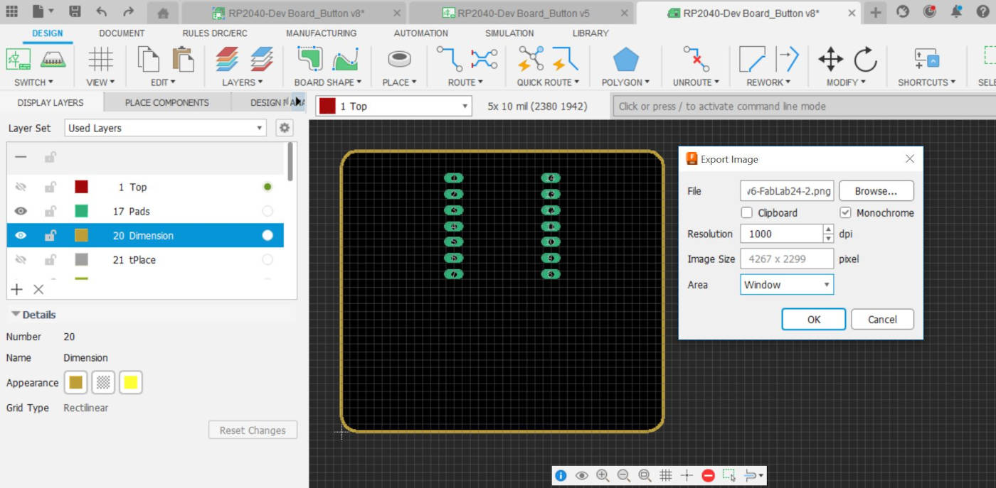
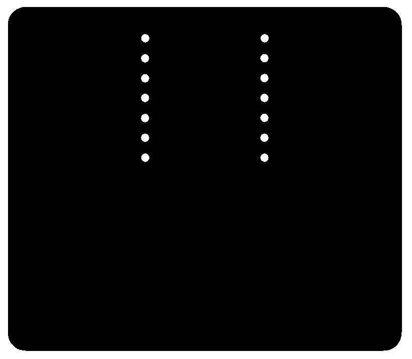
Once I finished exporting the image for the engraving of the paths, I proceeded to export the second image for the cut through. The process was the same, but this time I left ON the layer of the pads where the holes for the microcontroller are and the border outerline.
I opened the generated images in GIMP to touchup some minor details, for the engravig image I had to fill the holes of the pins.

|
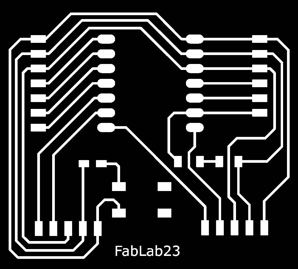
|
For the cut through image I had to leave only the holes for the pins and the outerline
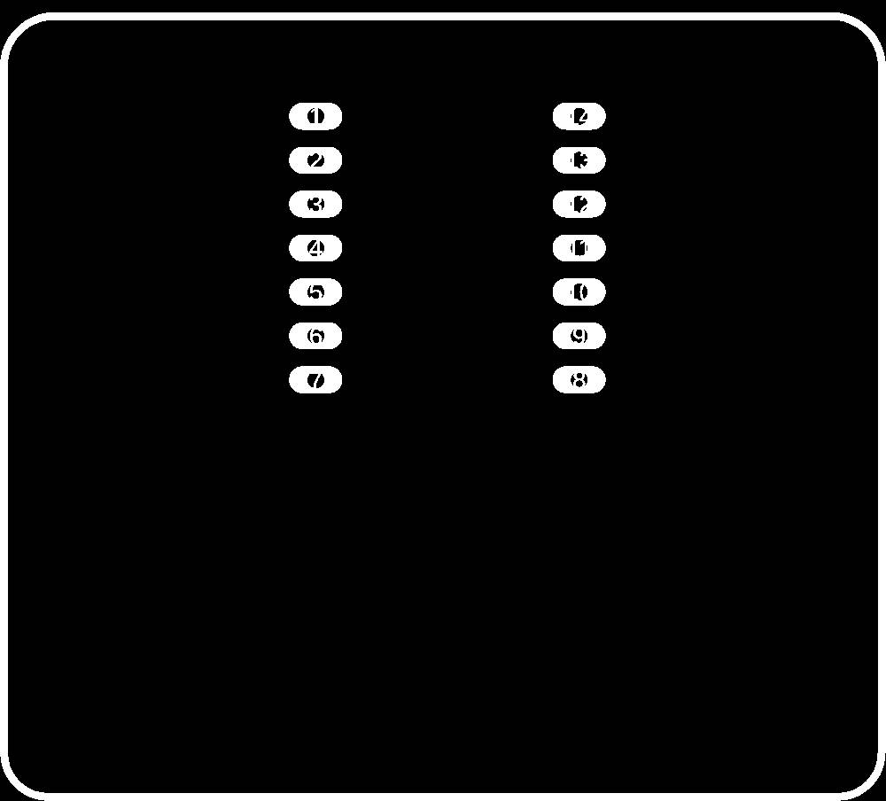
|
|
Having these two images I proceed to open the PNG images in Mods, and calculate them. This will generate the G-code I sent to the CNC machine to mill.
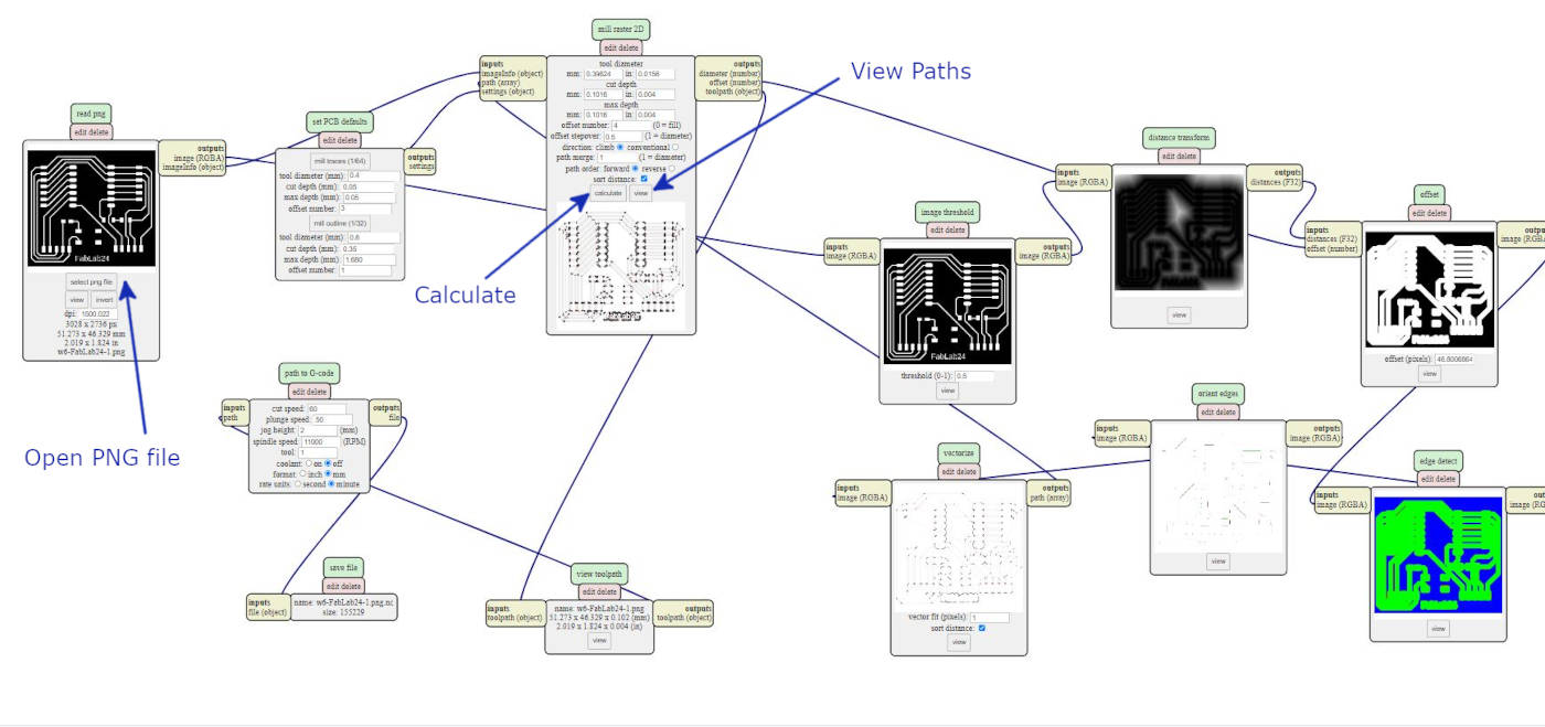
The steps to open mods are the following:
- Open MODS PAGE
- Right click on the screen and choose Programs from the menu
- Then choose Server Program from the list
- Scroll down to G-code, chose mill 2D PCB png
- Once Mods windows are opened we select open PNG file
- At the third window we select Calculate
- If we wish we can open to view the G-code path