Week 6: ELECTRONICS DESIGN

Group Assignment
- Use the test equipment in your lab to observe the operation of a microcontroller circuit board
Individual Assignment
- Design a development board to interact and communicate with an embedded microcontroller
- Extra-credit:Try another design workflow
- Extra-credit:Make a case for it
- Extra-credit:Simulate its operation
The group Assignment about use of testing equipments into our labs can found to fablab rwanda website . i personaly was familiar with test equipments from multimeter , oscilloscope ,function generator and many more. but this was good for my classmates who are not familliar with those equipment and i helped a lot with the testing
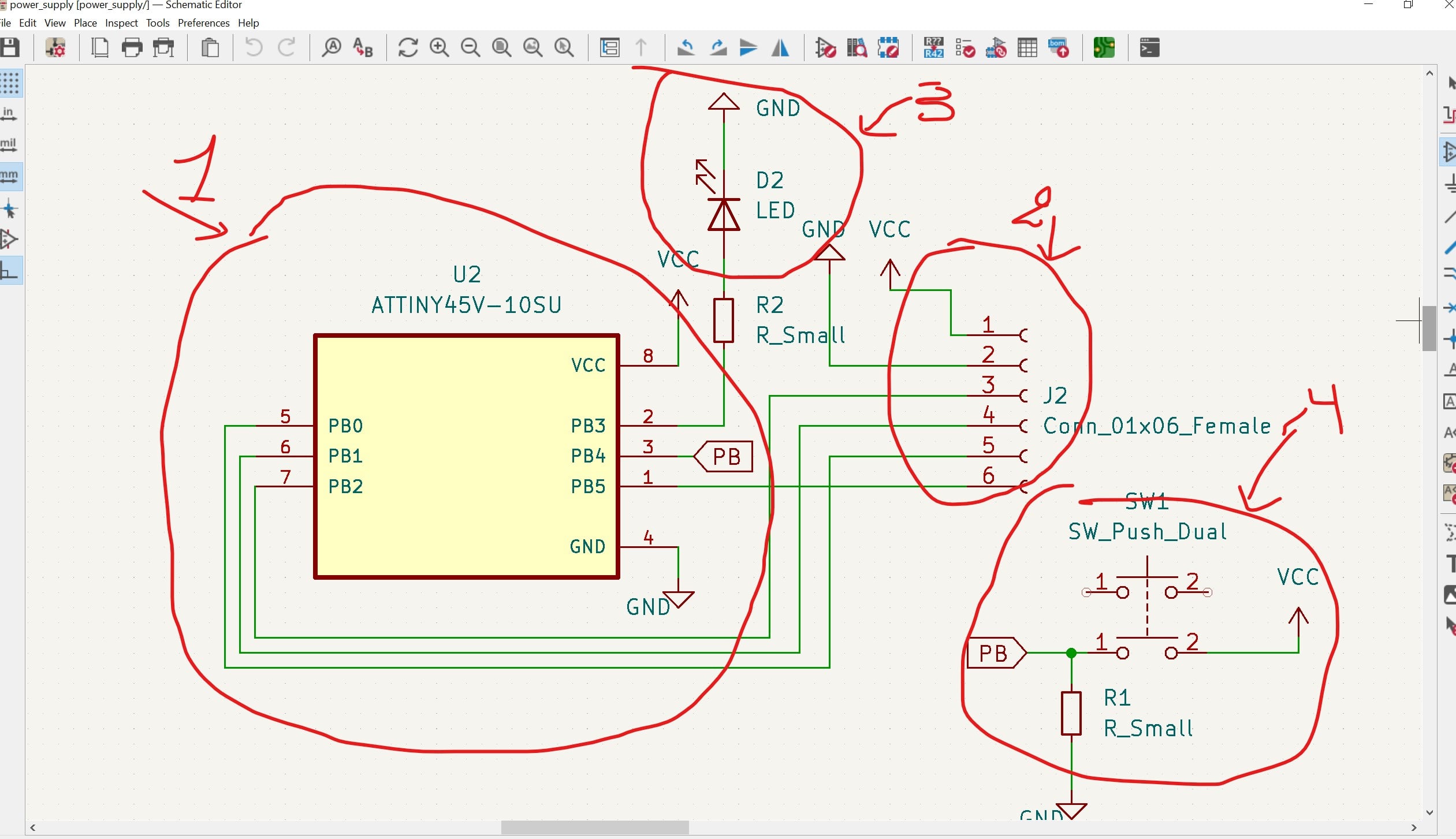
Make a development board and make it communicate
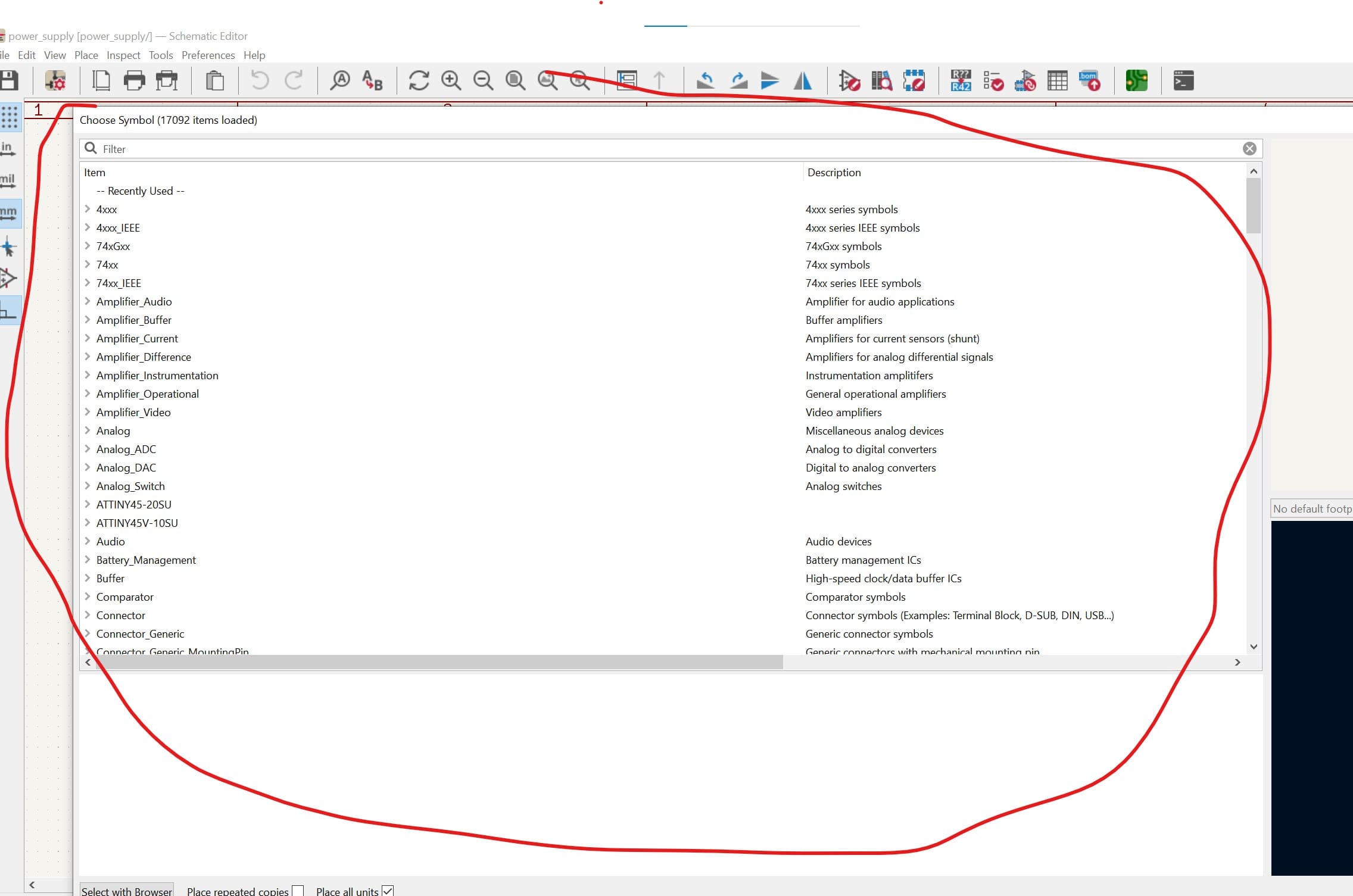
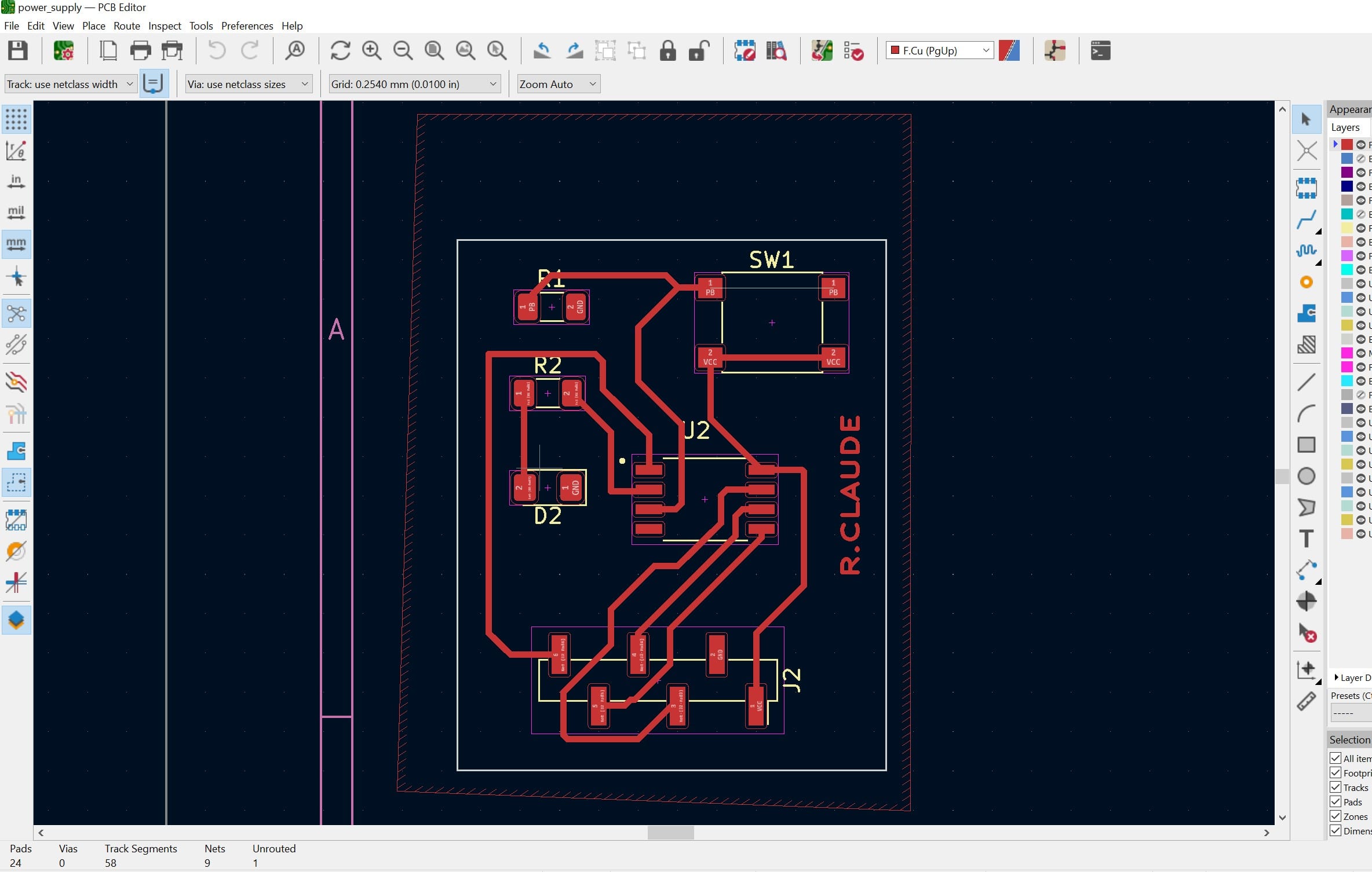
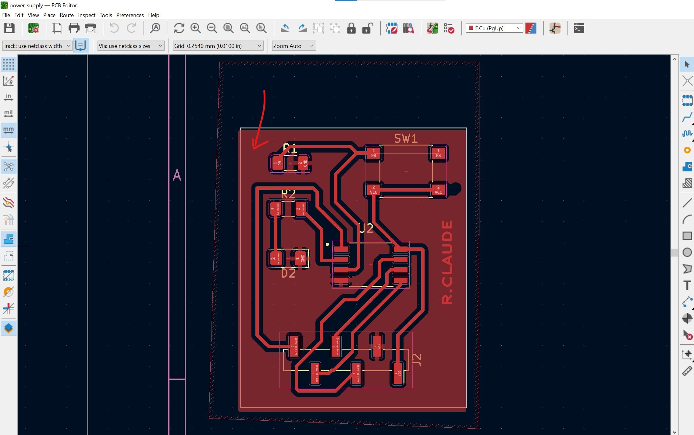
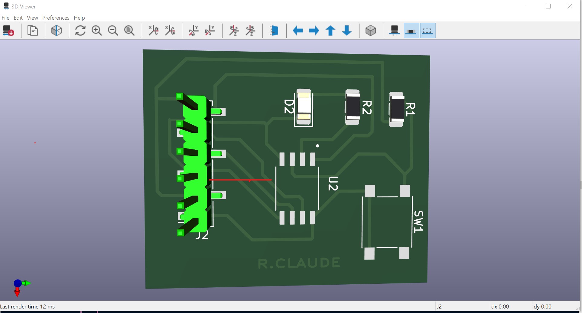
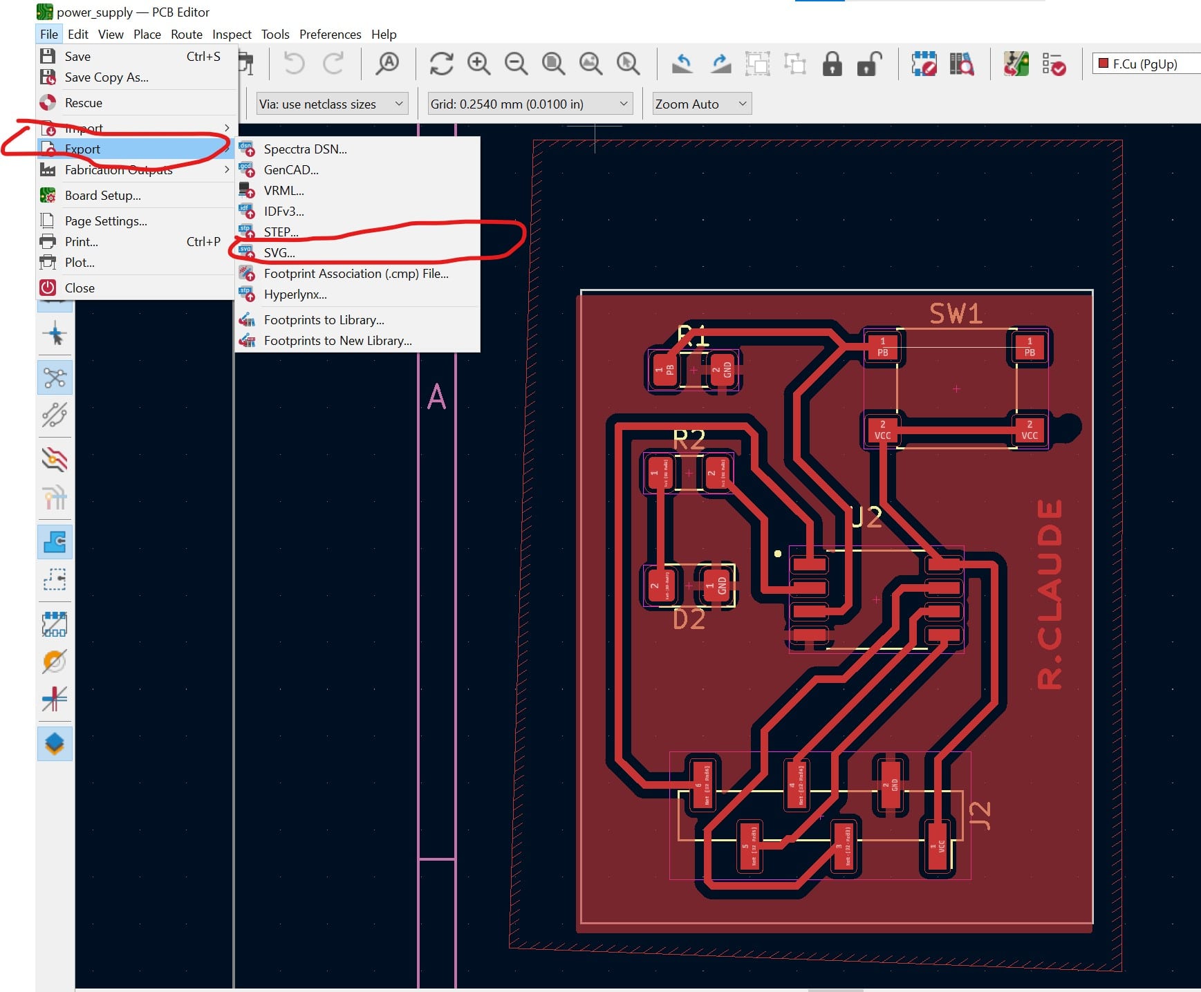
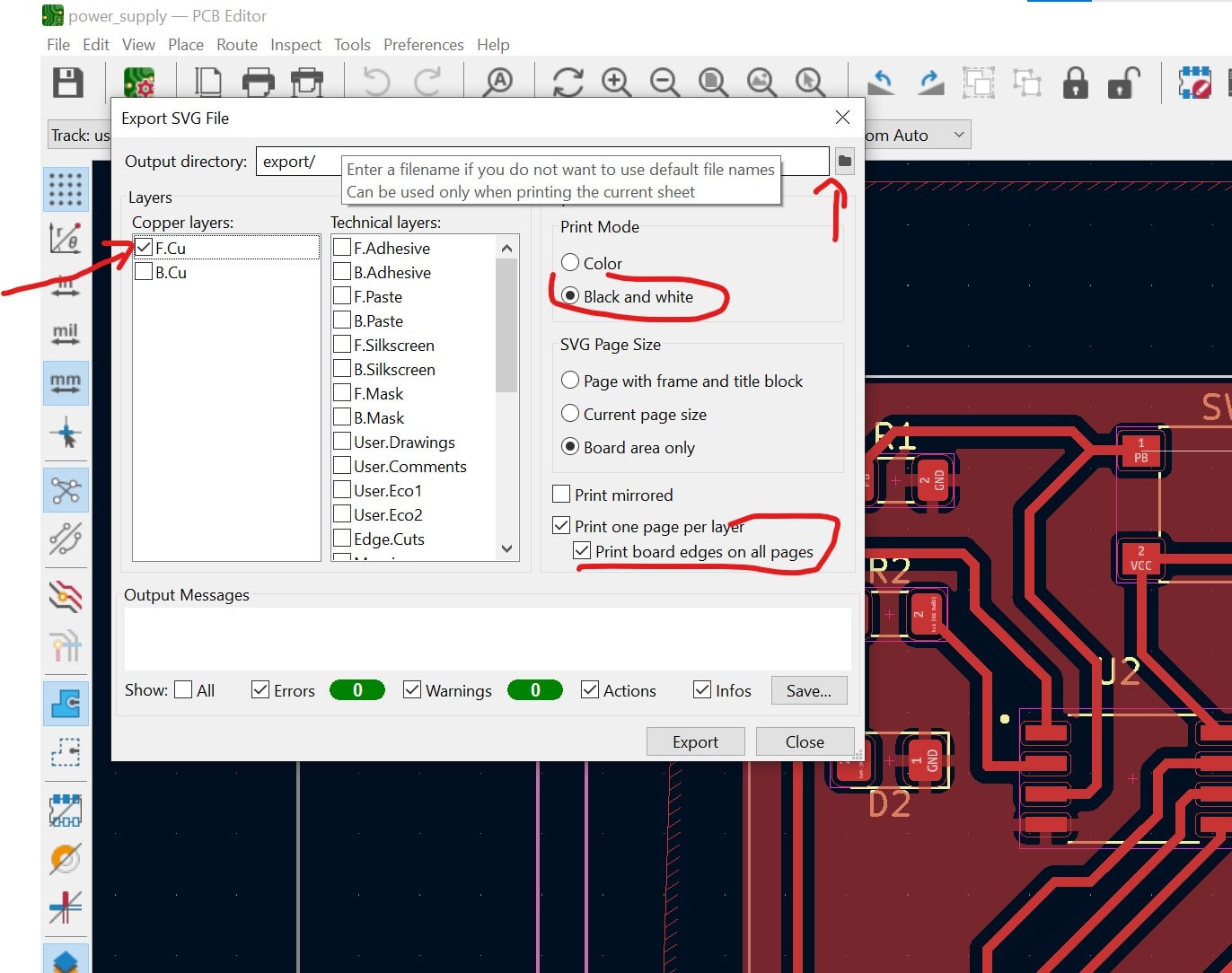
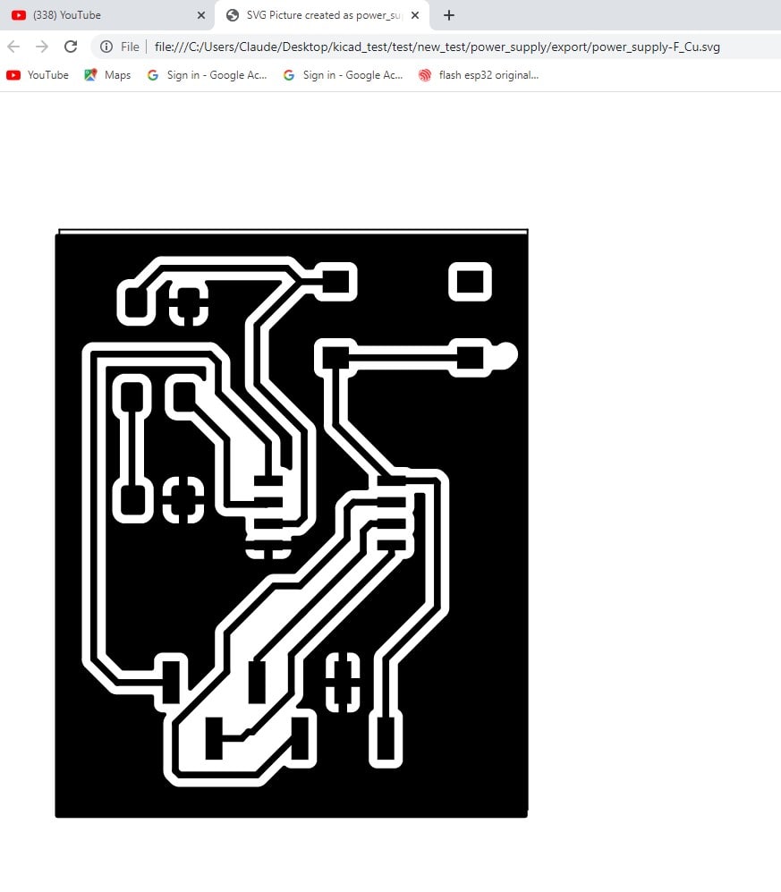
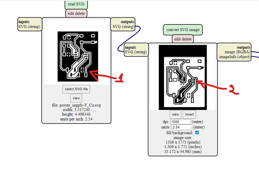
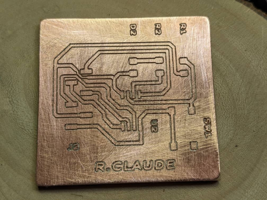
To design my circuit as indicated in the image bellow, i have used kicad which is free pcd tool that anyone can use. it is available for windows,mac and linux users . download it and install it
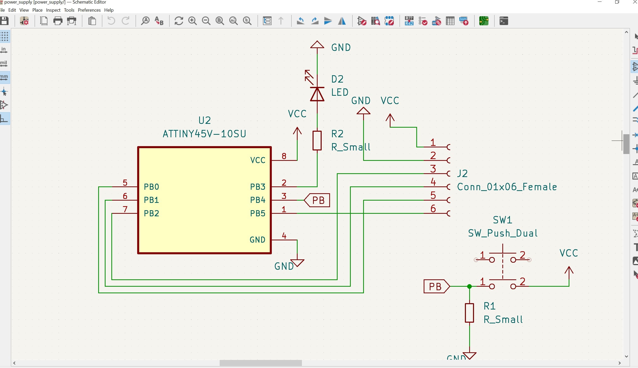
The following ar stpes to undergo while creating schematic and pcb in kicad
| Step | Description |
|---|---|
| Step 1 | Open KiCad and create a new project |
| Step 2 | Create a new schematic file within the project |
| Step 3 | Add components to the schematic by selecting them from the library and placing them on the schematic |
| Step 4 | Connect the components by drawing wires between them |
| Step 5 | Add any necessary labels or annotations to the schematic |
| Step 6 | Generate a netlist from the schematic |
| Step 7 | Create a new PCB file within the project |
| Step 8 | Import the netlist into the PCB file |
| Step 9 | Assign footprints to the components in the PCB file |
| Step 10 | Arrange the components on the PCB, ensuring that there is enough space for the traces to connect them |
| Step 11 | Route the traces between the components, using the autorouting tool or manually routing them |
| Step 12 | Add any necessary labels or annotations to the PCB |
| Step 13 | Check for errors and correct them as needed |
| Step 14 | Generate manufacturing files, including gerber files and drill files |
| Step 15 | Send the manufacturing files to a PCB manufacturer to produce the physical PCB |
Circuit Simulation
to simulate the working case of my circuit made with attiny45 with a push button and an LED , i have used an online tool called wokwi.com
Wokwi is an online platform that provides a virtual environment for designing, testing, and sharing electronics projects.
On Wokwi, users can design and simulate electronic circuits using a web-based schematic editor and a simulation tool that can simulate the behavior of the circuit in real-time. The platform supports a wide range of popular components and microcontrollers, such as Arduino, Raspberry Pi, ESP32, and more.
In addition to designing and simulating circuits, Wokwi also provides tools for sharing and collaborating on projects. Users can share their circuits with others by generating a unique link, embedding the circuit in a website, or exporting the design files for use in other software.
Wokwi only have attiny85 and it works the same as attiny45 that i have used in my circuit.
The following video illustrates the circuit simulation in wokwi
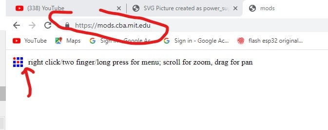
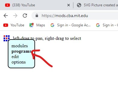
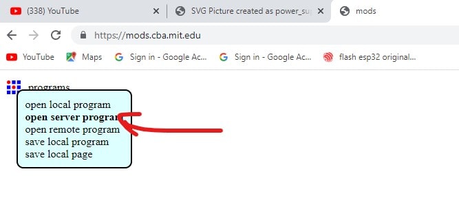
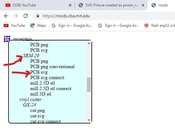
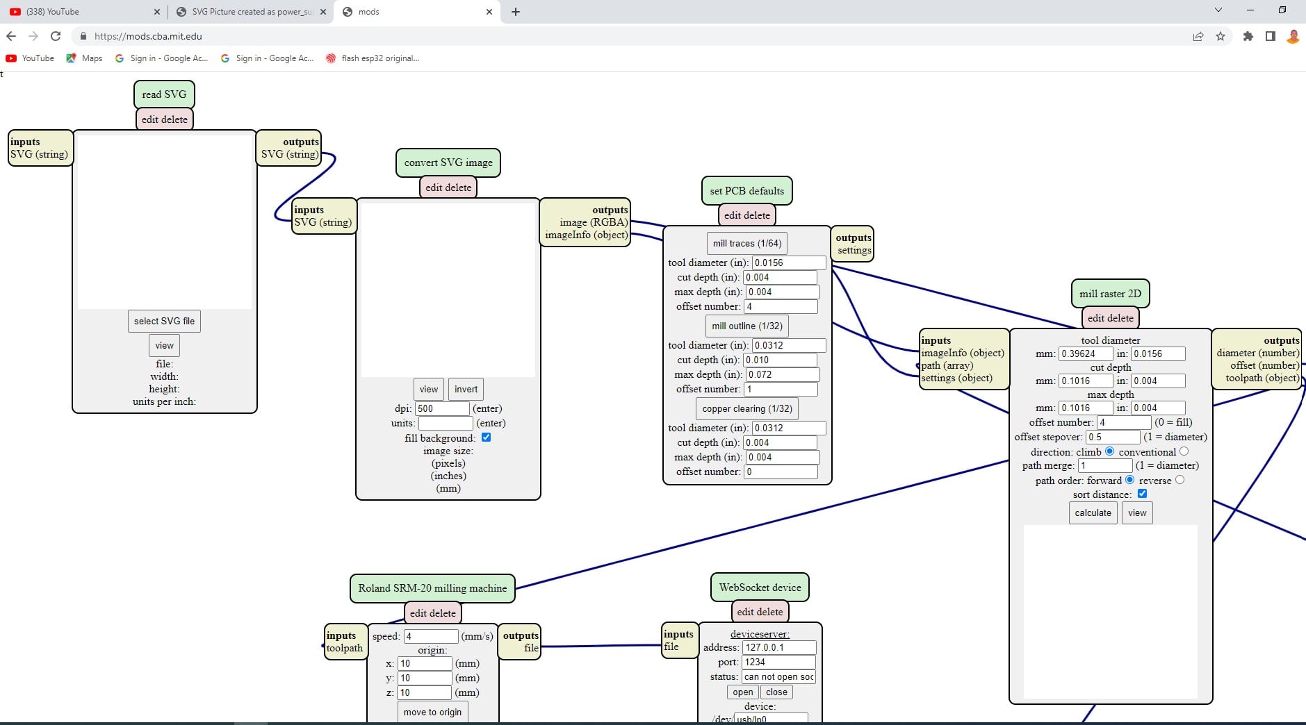
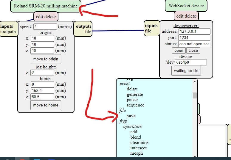
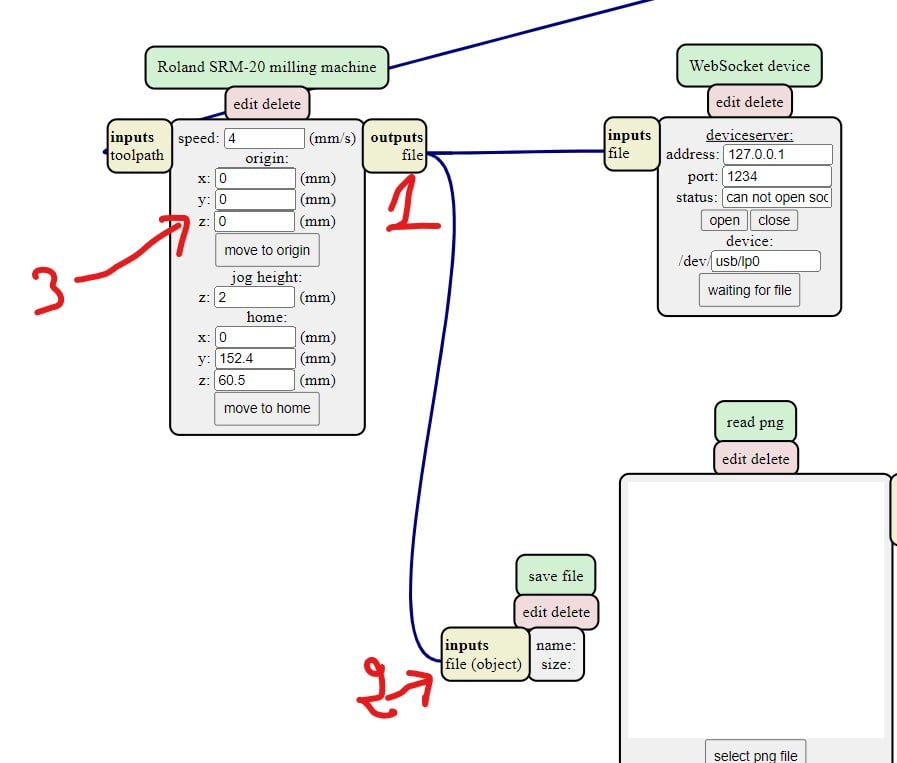
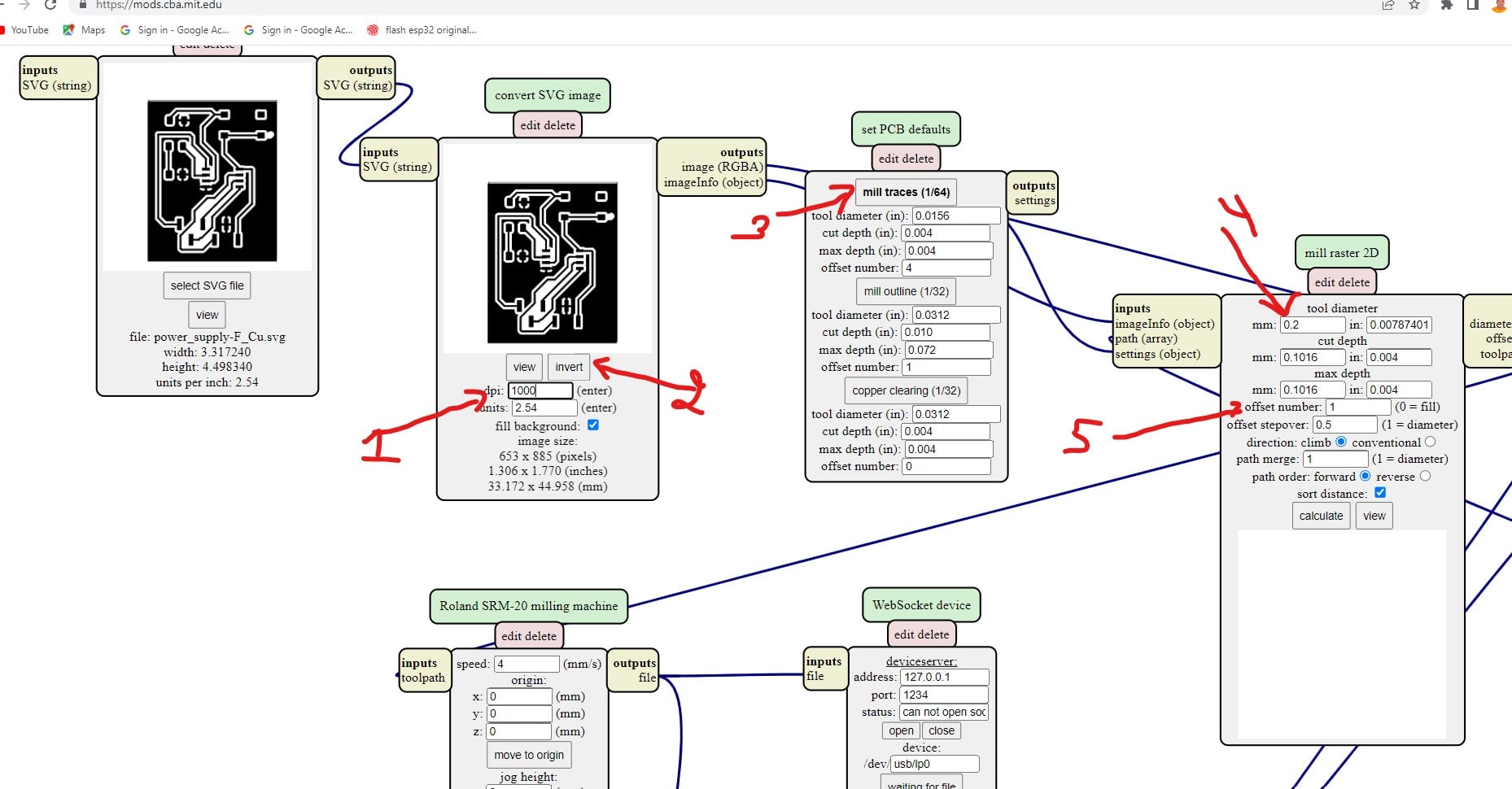
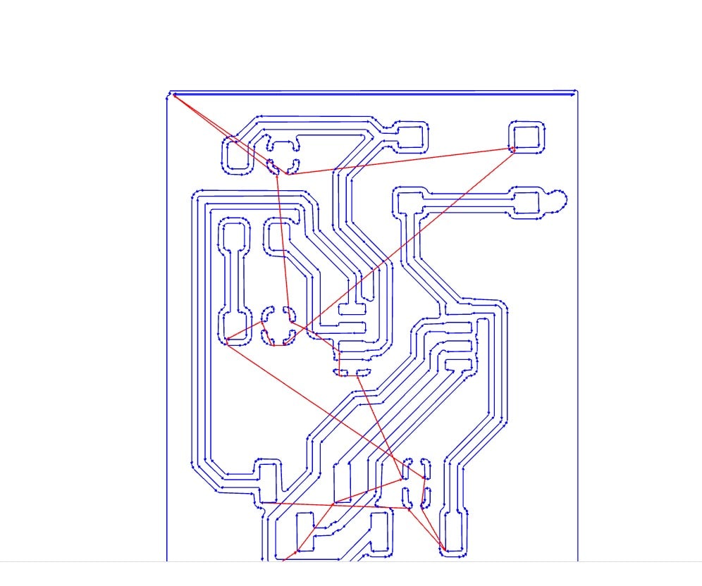
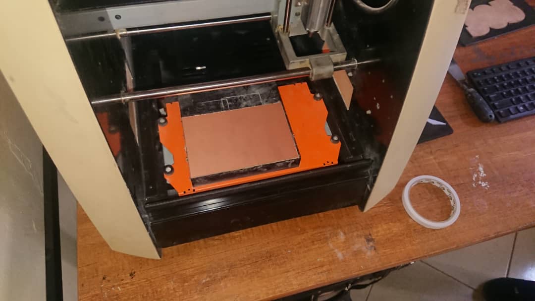
PCB Milling with Roland SRM-20 Milling machine
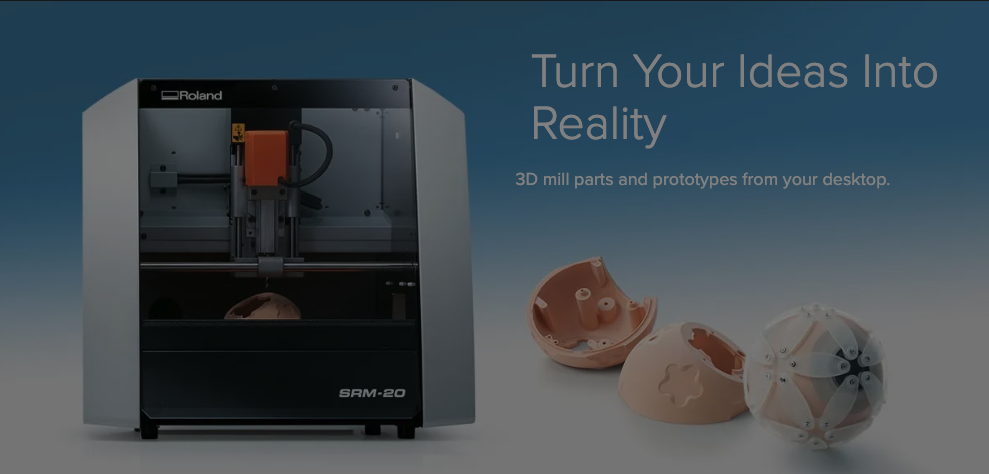
The Roland SRM-20 is a milling machine that is commonly used in Fablabs for PCB (printed circuit board) fabrication. It is a 3-axis milling machine that is capable of milling a variety of materials, including plastics, wood, and metals. The SRM-20 is known for its accuracy and precision, making it a popular choice for prototyping and small-scale production runs.
The SRM-20 is known for its ease of use and reliability, making it a popular choice for Fablabs and other makerspaces. It is also relatively affordable compared to other milling machines on the market, making it accessible to a wider range of users.To use the SRM-20 for PCB fabrication, the following steps are typically followed:
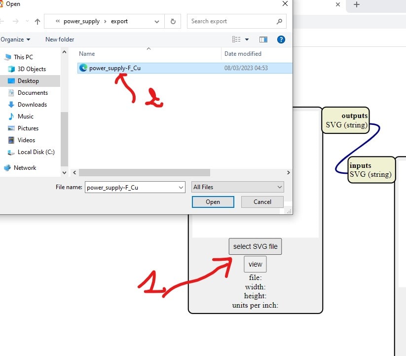
- Design the PCB layout using a software program such as Eagle, KiCAD, or Altium.
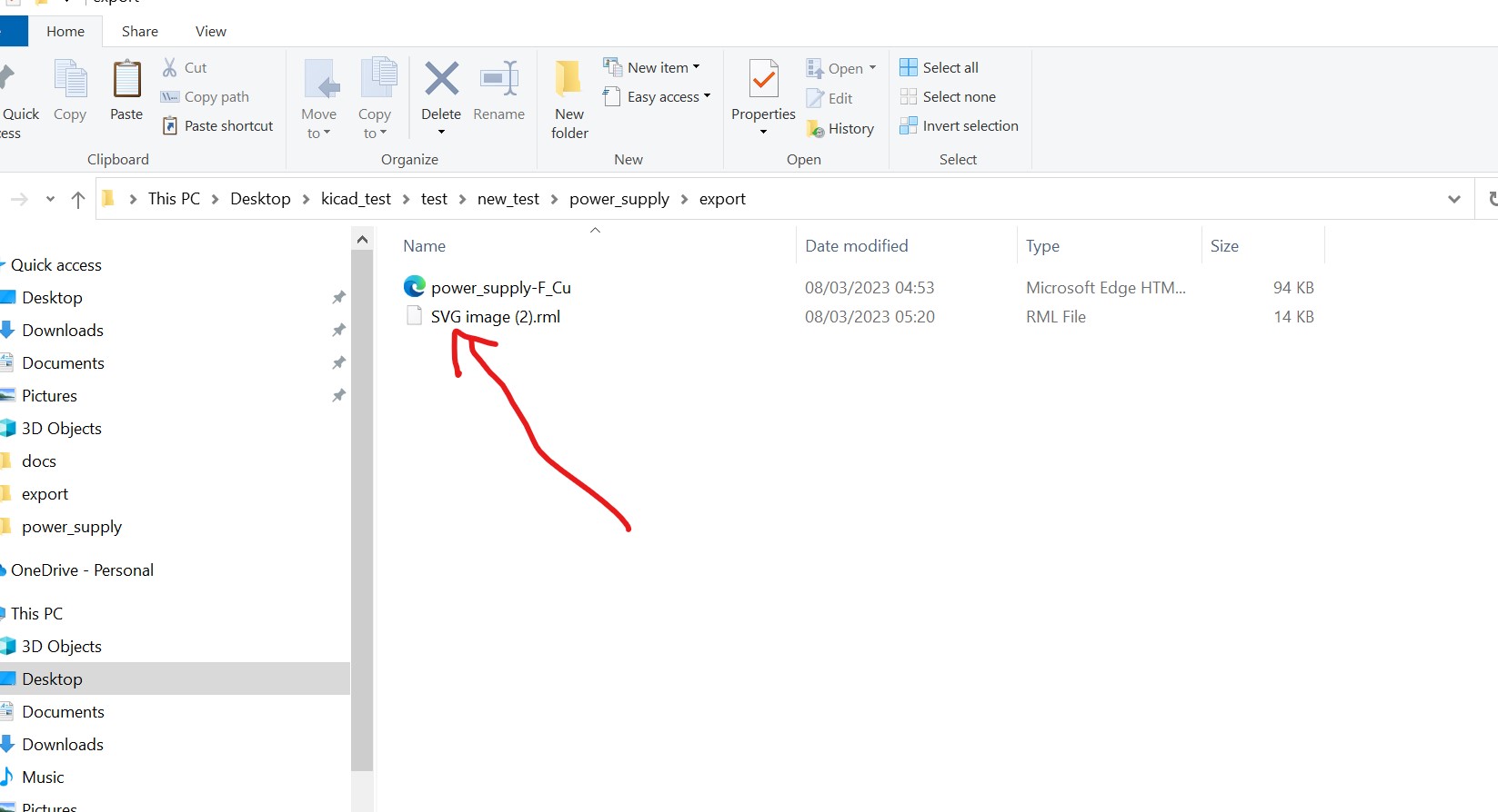
- Export the design file as a Gerber file, which contains the necessary information for the milling machine to create the PCB.
- Open the Roland SRM-20 milling machine and turn it on.
- Insert the material to be milled into the machine and secure it in place.
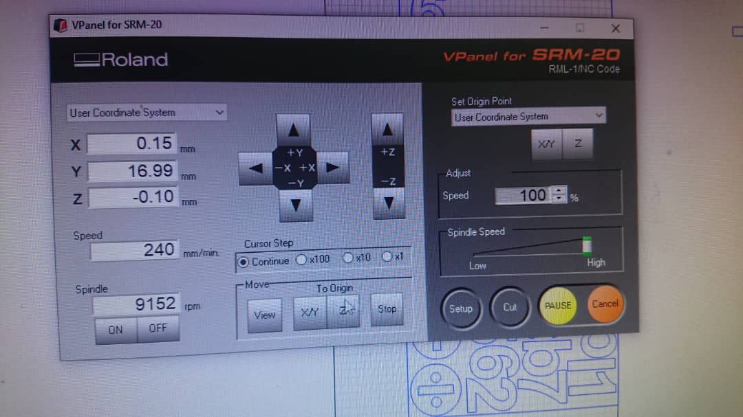
- Load the Gerber file into the milling software that comes with the machine.
- Set the milling parameters, such as milling depth and speed.
- Start the milling process.
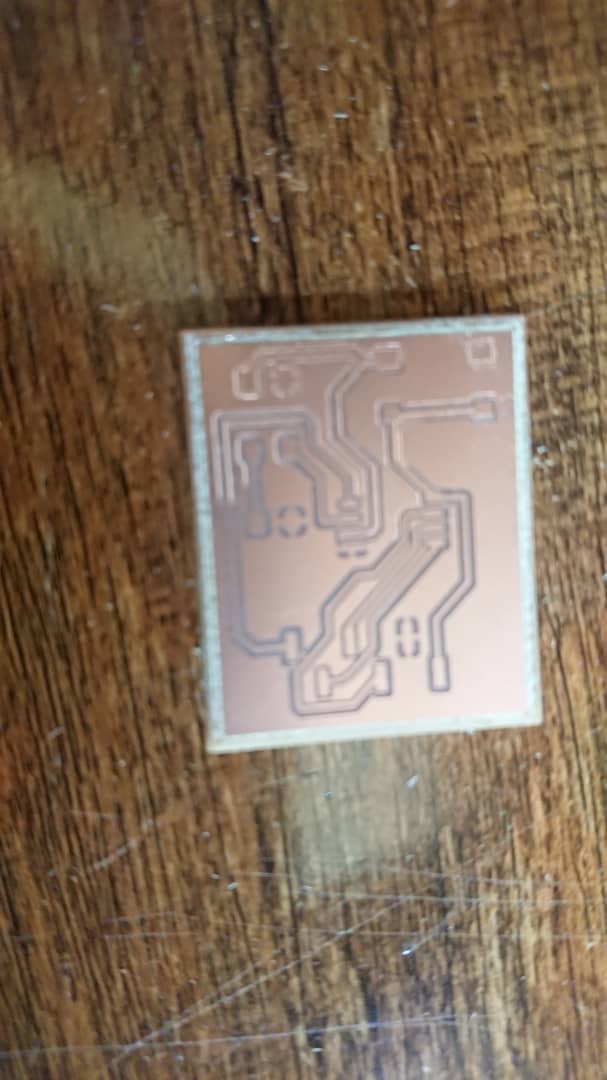
- Once the milling is complete, remove the PCB from the machine and inspect it for any defects.
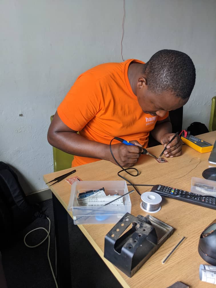
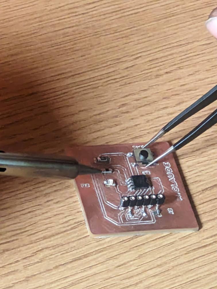
Burning a bootloader and program the Attiny45
After soldering, the next step was to make sure that the attiny45 runs correctly. we must load a biitloader first before running the first sketch
A bootloader is a small program that is used to load or initialize the main program or firmware of a microcontroller unit (MCU) or other electronic devices. The bootloader program is typically stored in a non-volatile memory, such as flash memory, of the MCU and it is executed when the device is powered on or reset. The main function of the bootloader is to prepare the MCU for the execution of the main program by initializing the required hardware resources and loading the main program into the appropriate memory locations.
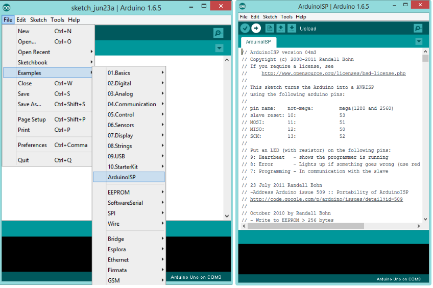
strongHere are the steps to burn bootloader in Attiny45 MCU using Arduino as ISP:
- Prepare the Arduino as ISP:
- Connect your Arduino to your computer using a USB cable.
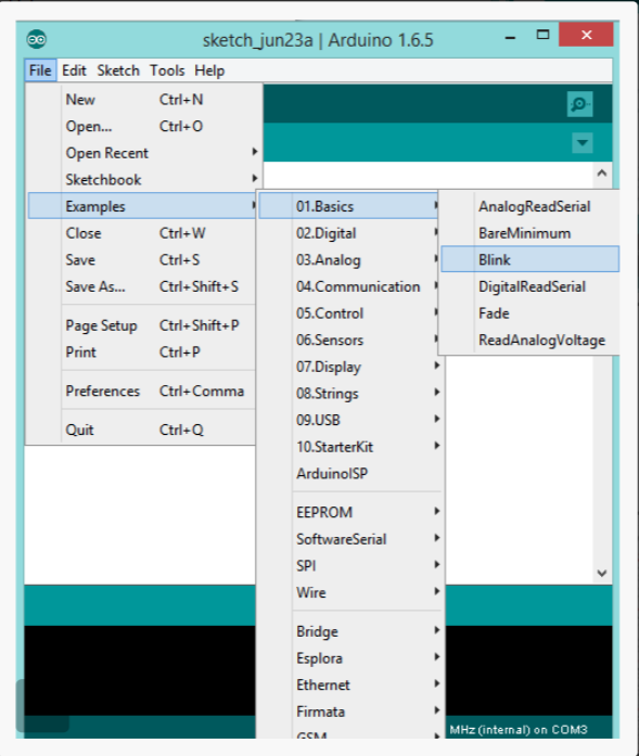
- Open the Arduino IDE and go to File > Examples > 11.ArduinoISP > ArduinoISP.
- Upload the sketch to your Arduino.
- Wire the Attiny45 to the Arduino:
- Connect the Attiny45 to the Arduino as follows:
- Attiny45 pin 1 to Arduino pin 10
- Attiny45 pin 4 to Arduino GND
- Attiny45 pin 5 to Arduino pin 11
- Attiny45 pin 6 to Arduino pin 12
- Attiny45 pin 7 to Arduino pin 13
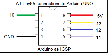
image credit to Intructables - Set up the Arduino IDE for Attiny45:
- Open the Arduino IDE and go to File > Preferences.
- In the Additional Boards Manager URLs field, enter the following URL:
- https://raw.githubusercontent.com/damellis/attiny/ide-1.6.x-boards-manager/package_damellis_attiny_index.json
- Click OK.
- Go to Tools > Board > Boards Manager.
- Search for "attiny" and install "ATTinyCore by SpenceKonde".
- Go to Tools > Board and select "ATtiny25/45/85".
- Go to Tools > Clock and select "Internal 8 MHz".
- Go to Tools > Programmer and select "Arduino as ISP".
- Burn the bootloader:
- Go to Tools > Burn Bootloader
- The IDE will start uploading the bootloader to the Attiny45 using the Arduino as ISP. This may take a few minutes.
- Once the bootloader has been uploaded, you will see a message in the IDE confirming the success of the process.
- Test the Attiny45:
- Disconnect the Attiny45 from the Arduino.
- Wire up the Attiny45 to your circuit as needed.
- Upload your sketch to the Attiny45 as you would with any other Arduino board.
- Your Attiny45 is now ready to use!
blink sketch. edit the sketch to use digital pin number 3 as output instead of LED_BUILTIN int ledPin =3; //Pin 3 //int ledpin =0; //Pin 5 void setup() { pinMode(ledPin, OUTPUT); } void loop() { digitalWrite(ledPin, HIGH); delay(500); digitalWrite(ledPin, LOW); delay(500); }
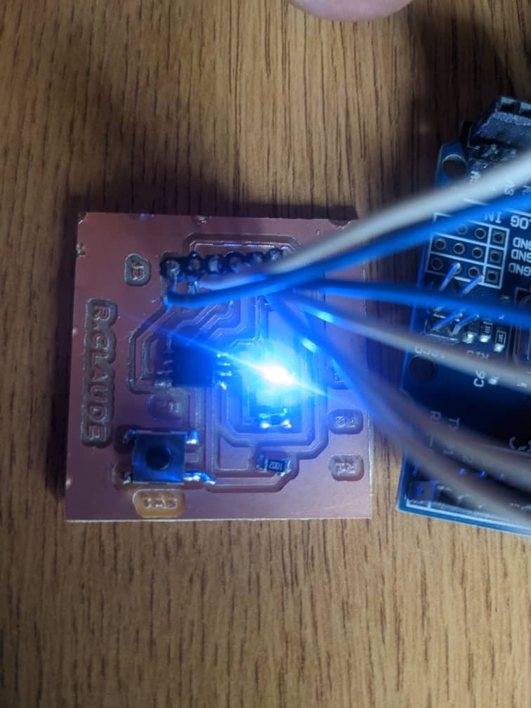
This video shows LED blinking