06. Electronics design
Part one : Assignments
-
Groupe assignment
- Use the test equipment in your lab to observe the operation of a microcontroller circuit board(as a minimum, you should demonstrate the use of a multimeter and oscilloscope).
- Document your work on the group work page and reflect what you learned on your individual page.
-
Individual project
- Design a development board to interact and communicate with an embedded microcontroller
Part two : Task
- Linked to the group assignment page.
- Documented what you have learned in electronics design
- Explained problems and how you fixed them
- Included original design files(Eagle, KiCad, etc.)
Part three : What I did
Groupe assignment
To see our group assignment click here
Individual project
1. What is Electronic Design Automation
Electronic design automation (EDA), also referred to as electronic computer-aided design (ECAD), is a category of software tools for designing electronic systems such as integrated circuits and printed circuit boards. It’s a set of software, hardware, and essential services for designing chips and semiconductor devices.
The sofware we are going to use is Eagle.
2. Install and use Eagle
EAGLE (Easily Applicable Graphical Layout Editor) is a flexible and expandable EDA schematic capture, PCB layout, autorouter and CAM program.
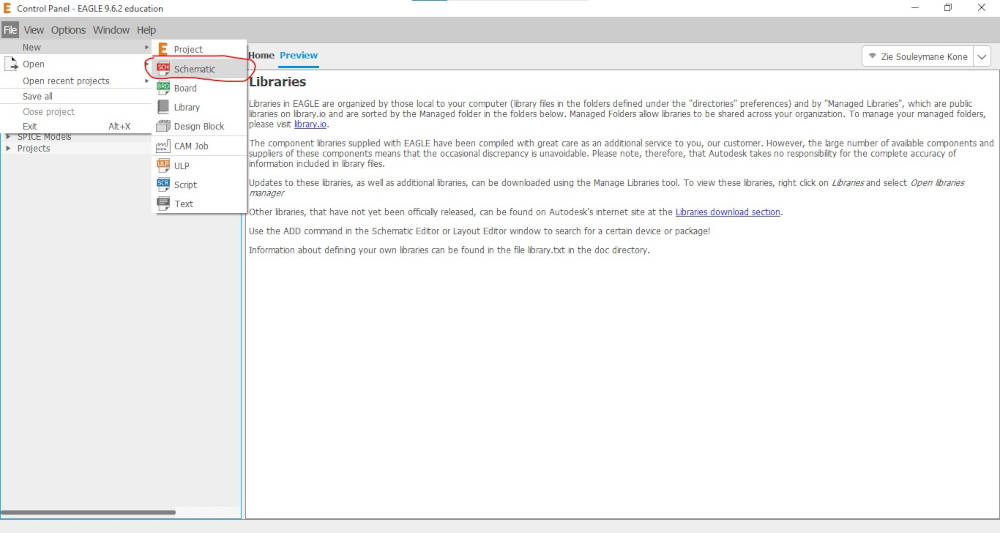
Step_01: Download and Install Eagle
- Download Eagle
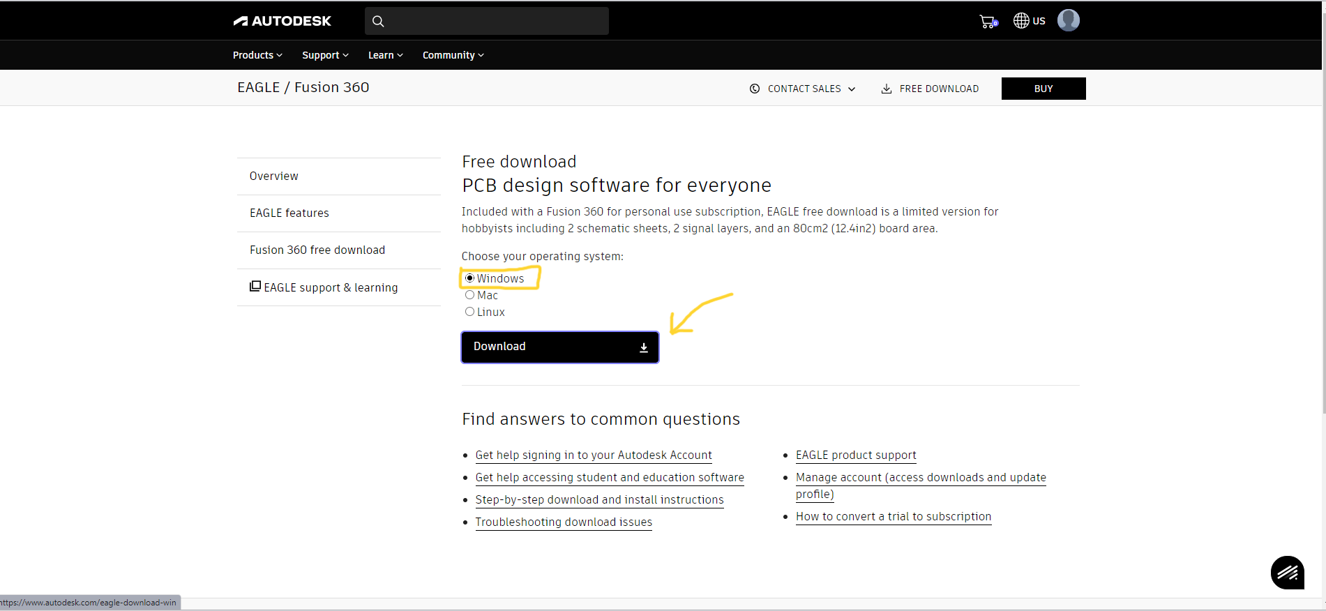
- Install Eagle
- Sign in
Step_02: Figure out issue here
-
Issue : (When launching/executing Autodesk EAGLE, the application:)
-
Navigate to “C:\EAGLE 9.x” and find the file “LIBEAY32.dll”.
-
Rename the .dll by appending .bak at the end of the file name: “LIBEAY32.dll.bak”.
-
Launch Eagle again, the program should open with no issue.
Step_03: Download and Install the component Libraries
- Download librarie files here
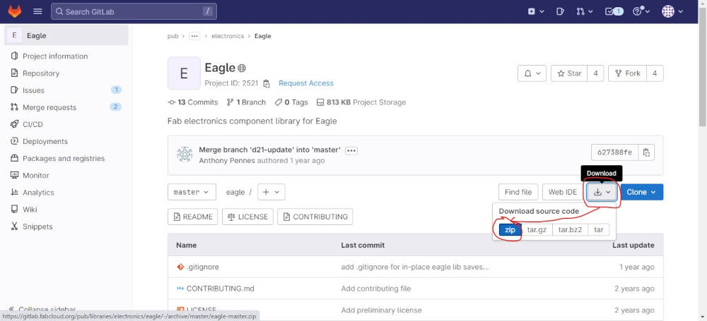
- Put the file fab.lbr , on Windows, on folder named Eagle\libraries


Step_04: How to Use Eagle
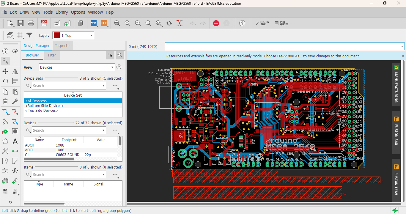
Eagle Basics
Eagle has two windows that you use simultaneously to design a board:
- Schematic (.sch)
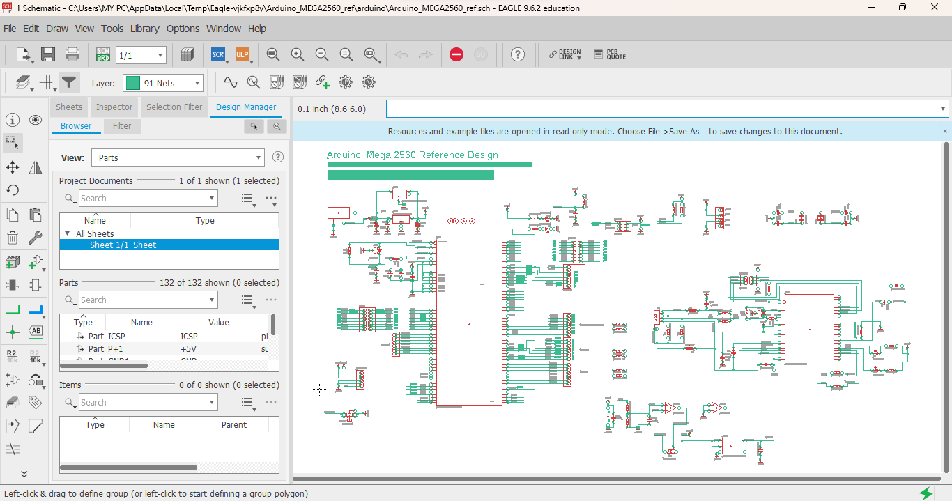
- Board Layout (.brd)
Working with the Eagle Interface
There are 2 ways to interact with Eagle.
-
Graphical Icons Toolbar: You can use the icons in the left-hand toolbar, mouse over them to see what they do. (enabled by default).
-
Command Line: You can start typing a command at any point, then select the item in the schematic / board that you wish to interact with, see section on commands below.
3. Design a development board Eagle
Data sheet : Seeed Studio XIAO ESP32-C3
- Presentation
Seeed Studio XIAO ESP32C3 is a development board for microcontrollers. It features an Espressif ESP32-C3 WiFi/Bluetooth dual-mode chip with a size of 20 x 17.5 mm, suitable for small projects and portable thanks to its low power consumption.
- Specification
| Item | Value |
|---|---|
| CPU | ESP32-C3 32-bit RISC-V @160MHz |
| Wireless Connectivity | WiFi and Bluetooth 5 (LE) |
| Flash Memory | 4MB |
| SRAM | 400KB |
| Digital I/O Pins | 11 |
| Analog I/O Pins | 4 |
| PWM Pins | 11 |
| I2C interface | 1 |
| SPI interface | 1 |
| UART interface | 2 |
| Power supply and downloading interface | Type-C |
| Power | 3.3V/5V DC |
| Dimensions | 20×17.5×3.5mm |
More information in this link. Here the Seeed Studio XIAO ESP32C3 pinout sheet.

- 5V: Supply voltage 5V.
- GND: Ground.
- 3V3: Supply voltage 3V3.
- Digital pins (GPIO Pin number): D0, D1, D2, D3, D4, D5, D6, D7, D8, D9, D10, D11
- Analog pins (GPIO Pin number): A0, A1, A2, A3
- SDA (GPIO Pin number): D4
- SCL (GPIO Pin number): D5
Note
Below are some important notes on the terminals of the XIAO ESP32C3 board, which should be taken into account when using it. For more details, click here.
- Terminal D9 of the XIAO ESP32C3 is connected to GPIO9 of the ESP32-C3, to a pull-up resistor and to the BOOT button. So pressing the BOOT button connects D9 to GND. It is therefore preferable to use D9 as a switching input.
- D6 on the ESP32C3 XIAO is connected to U0TXD (28) on the ESP32-C3. D’ou D6 is configured as a UART output at start-up, so if you use D6 as an input, you may accidentally generate a high current. So it is recommended to use the D6 pin only in output mode.
BOM and Schematic
Samdino |
Where to buy? | Amount | Price | Total price |
| Proto Board FR1 | Digikey | 1/4 board | 1,24 €/unit | 0,31 € |
| Seeed Studio XIAO ESP32C3 | Seeed Studio | 1 | 5,00 €/unit | 5,00 € |
| 499 Ω resistor | Digikey | 1 | 0,09 €/unit | 0,09 € |
| 1kΩ resistor | Digikey | 1 | 0,09 €/unit | 0,09 € |
| LED | Digikey | 1 | 0,35 €/unit | 0,35 € |
| Button | Digikey | 1 | 1,00 €/unit | 1,00 € |
| Female 1 row horizontal header | Digikey | 3 | 0,15 €/unit | 0,45 € |
| Total cost | 7,29 € |
Design
Step_01 : Open Autodesk Eagle click on File>New>Schematic
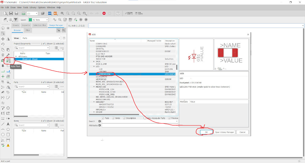
Step_02 : Click on the Add Part button and select the LEDFAB1206 component as shown below.
Step_03 : Once you’ve added all the components, click on Net to connect them as shown below.

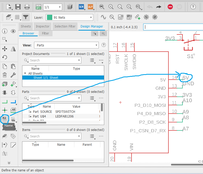
Step_04 : Click on Name and rename the green lines as shown below.
Step_05 : We repeat all the above procedures to obtain the final result below
We have finished the drawing of the electronic schematic and now we will draw the PCB.
Step_06 : After positioning the components correctly and resizing the edges of the PCB. Select the “Route Airwire” tool and draw the various circuit tracks as shown below.
Here are the final results of our design
4. Generation of PNG files for the traces and the board outline
Once I have all the components placed and the tracks together, I need to export the file as a “.PNG”. But first we need to be only exported the tracks, and after the outlines. To do this we followed the process below:
Step_01 : Click on “Layer Settings”, uncheck all but “Top” and click on “OK”.
Step_02 : Go to File>Export and click on “Image” a window will open, click on “Browse…” to choose the file type and location, select “Monochrome” with Resolution = 1000 dpi and click on “OK”.
Step_03 : Repeat the same procedure as above and in “layer settings” select “Dimension” instead of “Top”.
You should have the results below.
5. Design a development board Kicad
I continued my work on KICAD because I have some notion of design with the software so I found it useful to deepen my knowledge using this software.
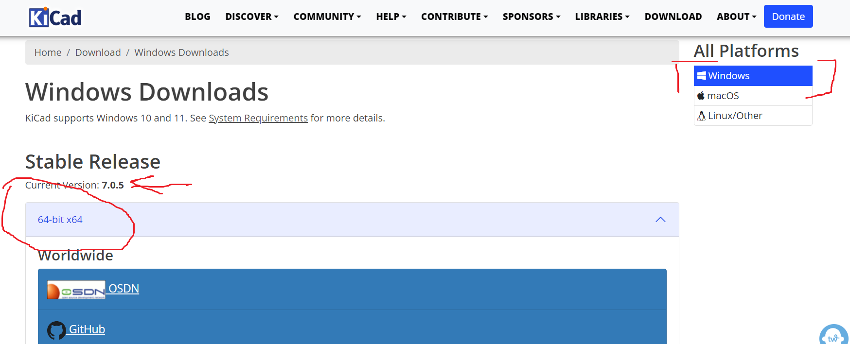
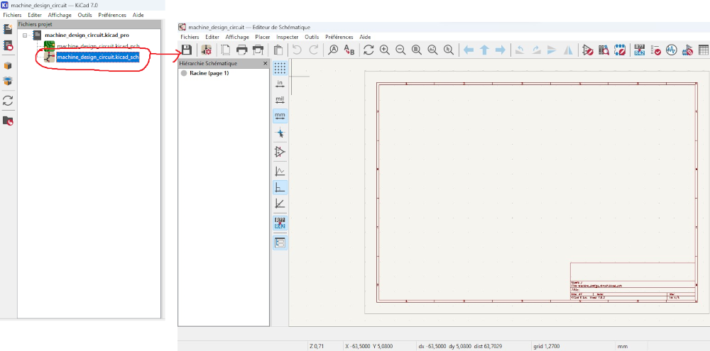
- Open KiCad 7.0 click on File>New project

- Double left-click on the file circled in red below to access the electronic schematic entry page.
-
To add components, click on the icon circled in red. A window will open, select your component, click on ok and place it in the schematic input zone as shown below.
-
After placing the component, we used the “add a net label (L)” tool as shown above. to use it, click on it and enter the markers of the terminals you want to use as shown below.

- Now we’re going to connect the XIAO’s GND terminal to the GND label. To do this, position yourself on the end of the XIAO’s GND terminal as shown below and click on it, then move the mouse to the GND label terminal and click a second time on the mouse.
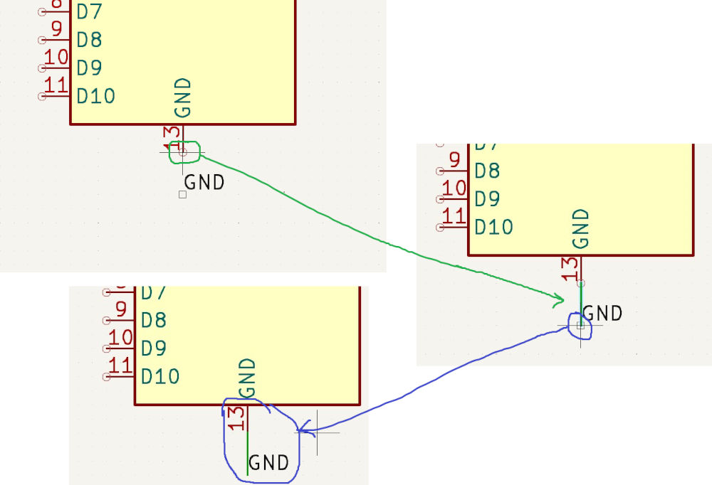
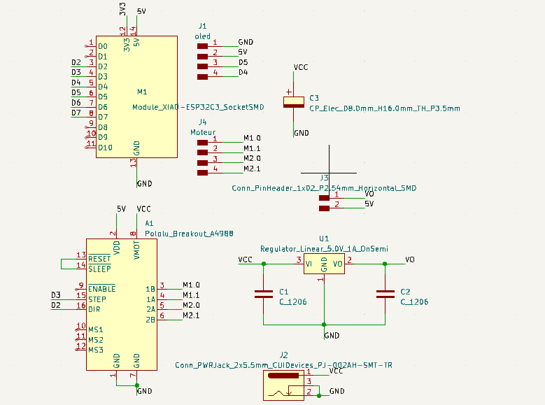
- After following and repeating the steps described above, we obtained the following result.
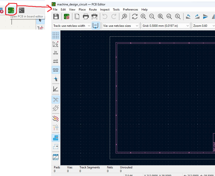
Now that we’ve finished the circuit diagram, we’ll move on to the PCB design. To do this, click on the icon circled in red below.
- Once the PCB window is open, click on the icon circled in red below, then on update and on close, and place the traces of the various components where you want them, as shown below.

Once you have positioned the components correctly and resized the edges of the PCB as shown above, click on “route tracks (X)” to trace the PCB tracks as shown below.

- After tracing all the tracks on the printed circuit board, we obtained the result below.

Board traces Net classes setting
To enter in the Net classes settings follow the steps below :
1.
 Click on the drop-down menu circled and select the last option Edit Pre-defined Sizes
In the window which is displayed go to the net classes setting you should get this window below if all is well.
Click on the drop-down menu circled and select the last option Edit Pre-defined Sizes
In the window which is displayed go to the net classes setting you should get this window below if all is well.

We’ve highlighted on the picture above the section where we put the differents parameters.
-
The first parameter is the clearance : That is the parameter defining the minimum spacement between the components. It prevents accidental shorts or electrical interference between traces. This parameter helps you define how much space should be left between elements belonging to different nets within this net class.
-
Then we have the track width which is naturally the width of the tracks.
-
Via Size represent the diameter of the hole.
-
Via hole This is the deep of the hole that will be drilled for vias.
-
DP Gap or Differential Pair Gap is for differential pairs, this parameter sets the minimum separation between the two traces of the pair.
In accordance with the tools we use, certain parameters have been set, as indicated above. The diameter of the traces tool is 1/64”, approximately 0.4mm. Therefore, we need to define the clearance as greater than or equal to 0.4.
For the cutting process, the size of the outside line should be around 0.8mm since the tool’s diameter is 1/32”, approximately 0.8mm. For this, all hole diameters must be at least 1/64”. Otherwise, toolpath generators like Mods will not be able to calculate the toolpath.
Generation of SVG files for the traces and the board outline
Once all the components have been placed and the tracks assembled, I need to export the file in “.SVG” format. We exported only the tracks, then the contours. To do this, we follow the procedure below:
- Click on File> Export> SVG…
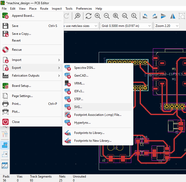
- First, we’ll export the PCB traces.To do this, in the export window, check the “F.Cu” , “Black and White” and “Board area only” boxes as shown below and click on Export.
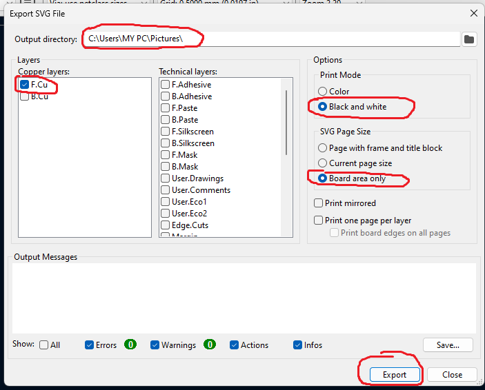
- To export the PCB contours and holes, check the “B.Cu” , “Edge.Cuts”, “Black and White” and “Board area only” boxes as shown below and click on Export.

Below is an image of the export results. To obtain the design and SVG source files for the printed circuit board, go to the Files section at the end of the page.
