08. Electronics production
Hero Shots
Assignment Requirements
Group assignment
- Characterize the design rules for your in-house PCB production process: document feeds, speeds, plunge rate, depth of cut (traces and outline) and tooling.
- Document your work to the group work page and reflect on your individual page what you learned
Link to group assignment page
The group assignment page can be found on the Energylab 2023 website here
it is also embedded directly in the webpage below.
Individual assignment
- Make and test the development board that you designed to interact and communicate with an embedded microcontroller
Group Assignment
Requirements:
- Characterize the design rules for your in-house PCB production process: document feeds, speeds, plunge rate, depth of cut (traces and outline) and tooling.
- Document your work to the group work page and reflect on your individual page what you learned
Individual assignment
Requirements:
Make and test the development board that you designed to interact and communicate with an embedded microcontroller
Workflow
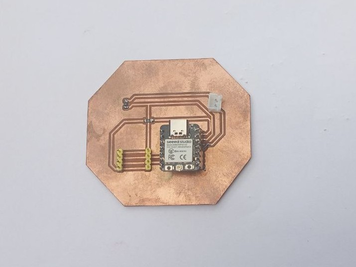
This week, we’re going to produce the electronic design of my 2 boards that we made with “Kicad” in week 6.
Step 1: Generate the Gcode with Flatcam
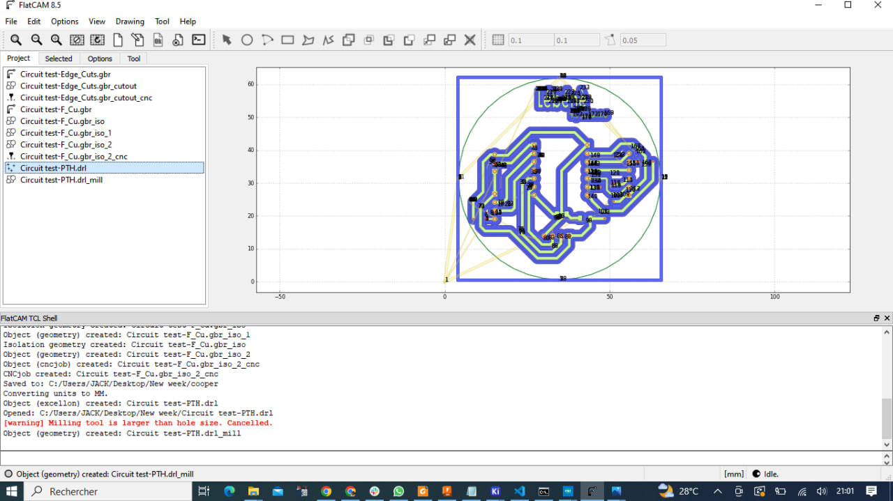
For this first step, we’ll be using the “Flatcam” software to generate the Gcode for our design, which will enable us to cut out our PCB board. At the end of this operation, we’ll have generated 3 gcodes. A first gcode will create the holes on our board, a second will trace the tracks and a third will cut the shape of our PCB.
The total thickness of the copper plate we have in our fablab for this job is 1.40 mm. Including 0.4 mm of copper above 1 mm of bakelite.
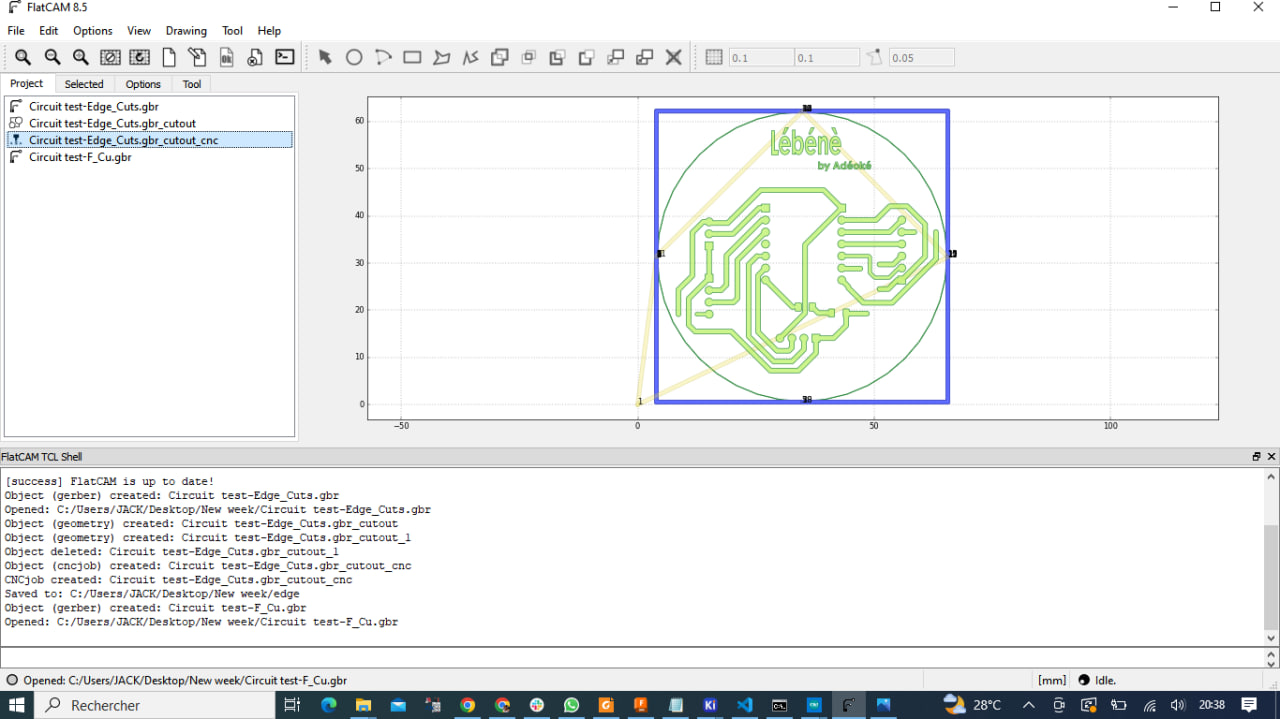
After opening the “Flatcam” software, we loaded our first “Edge cut” file to generate its gcode.
Then we double-click on the file name
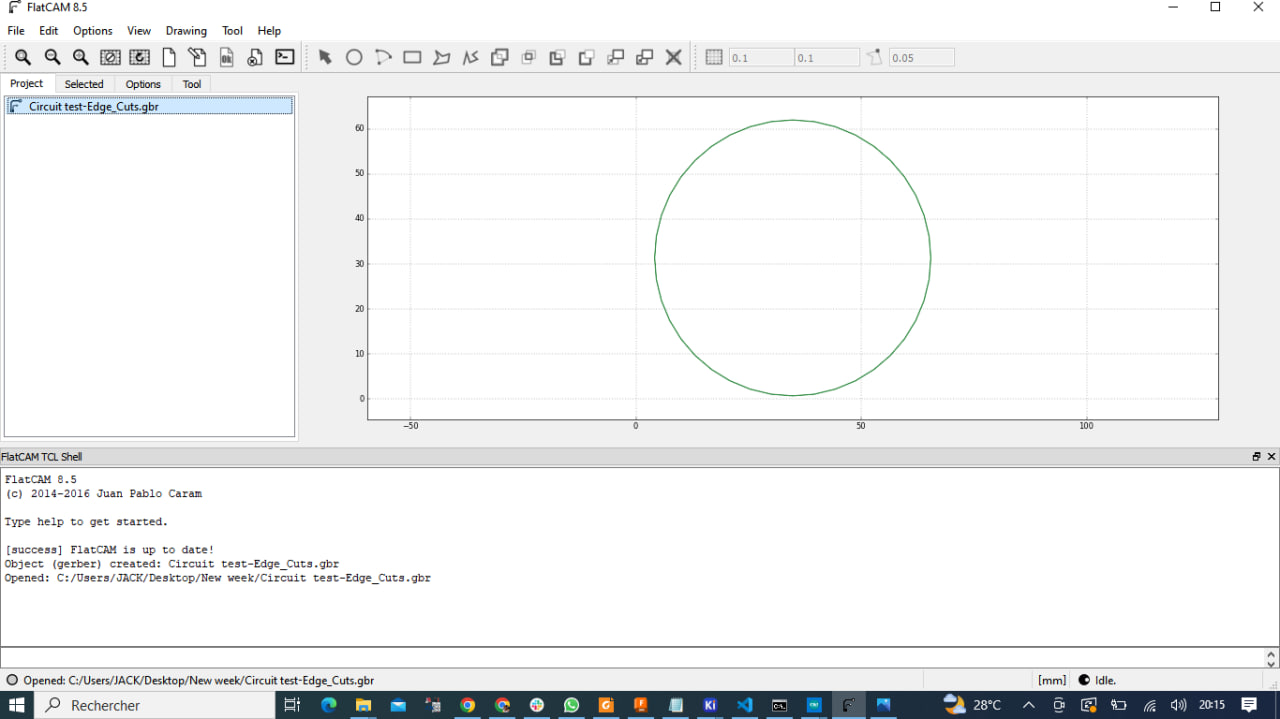
A new window opens, in which we insert the various parameters for cutting the shape of our PCB. Then click on “Generate” to generate the shape.
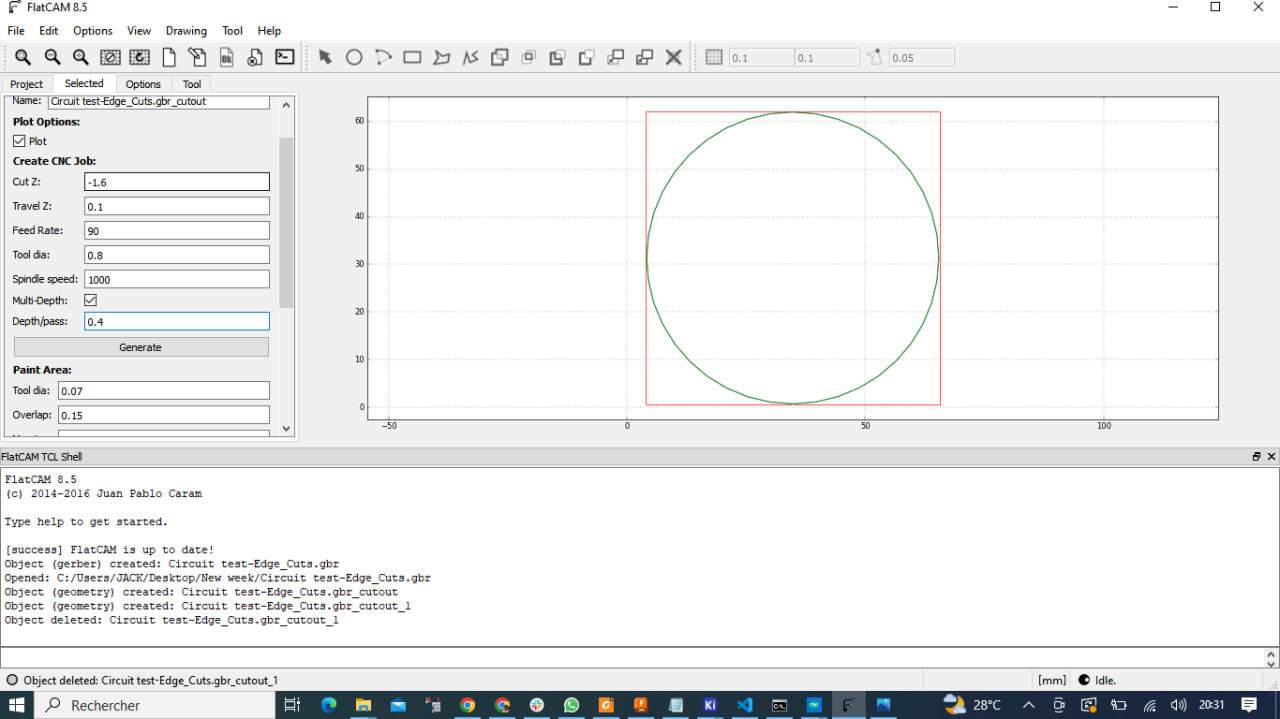
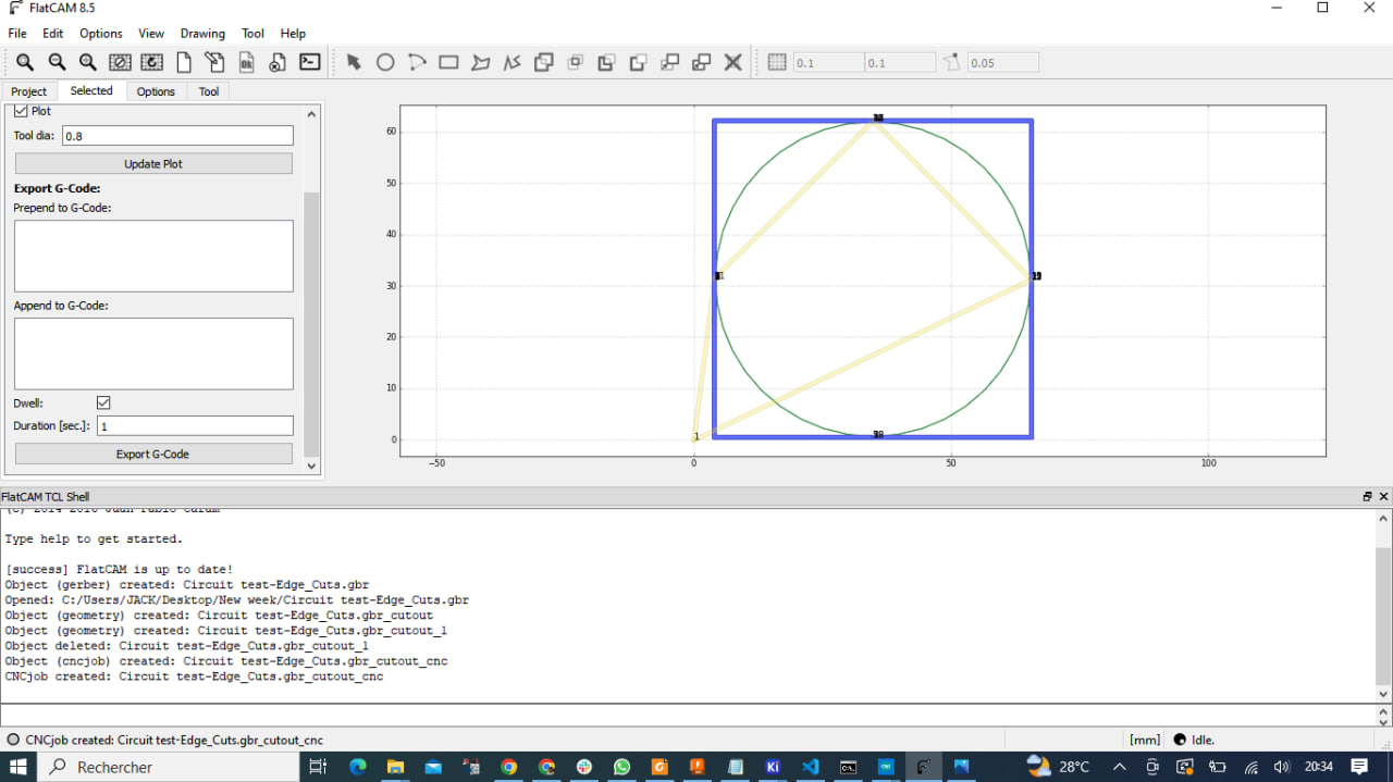
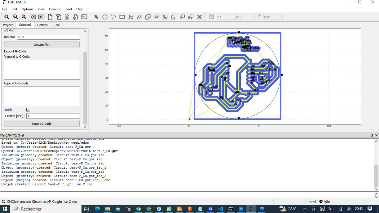
After generating the shape, we double-click again on the generated shape file, and a new window opens again. Insert the parameter values and click on “Export Gcode” to generate the Gcode.
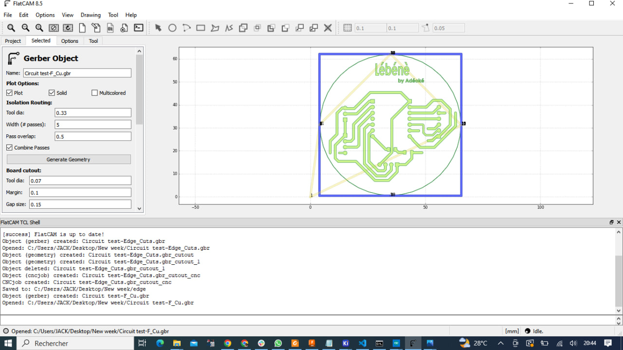
Here are the main parameters I used for “Edge Cut”
| Parameter | Value |
|---|---|
| Cut Z | -1.6 mm |
| Travel Z | 0.1 mm |
| Feed rate | 90 mm/min |
| Tool diameter | 0.8 mm |
| Spindle speed | 1000 mm/min |
| Depth/pass | 0.4 mm |
To generate the Gcode for track tracing, repeat the process as before, taking care to enter the correct parameter values.
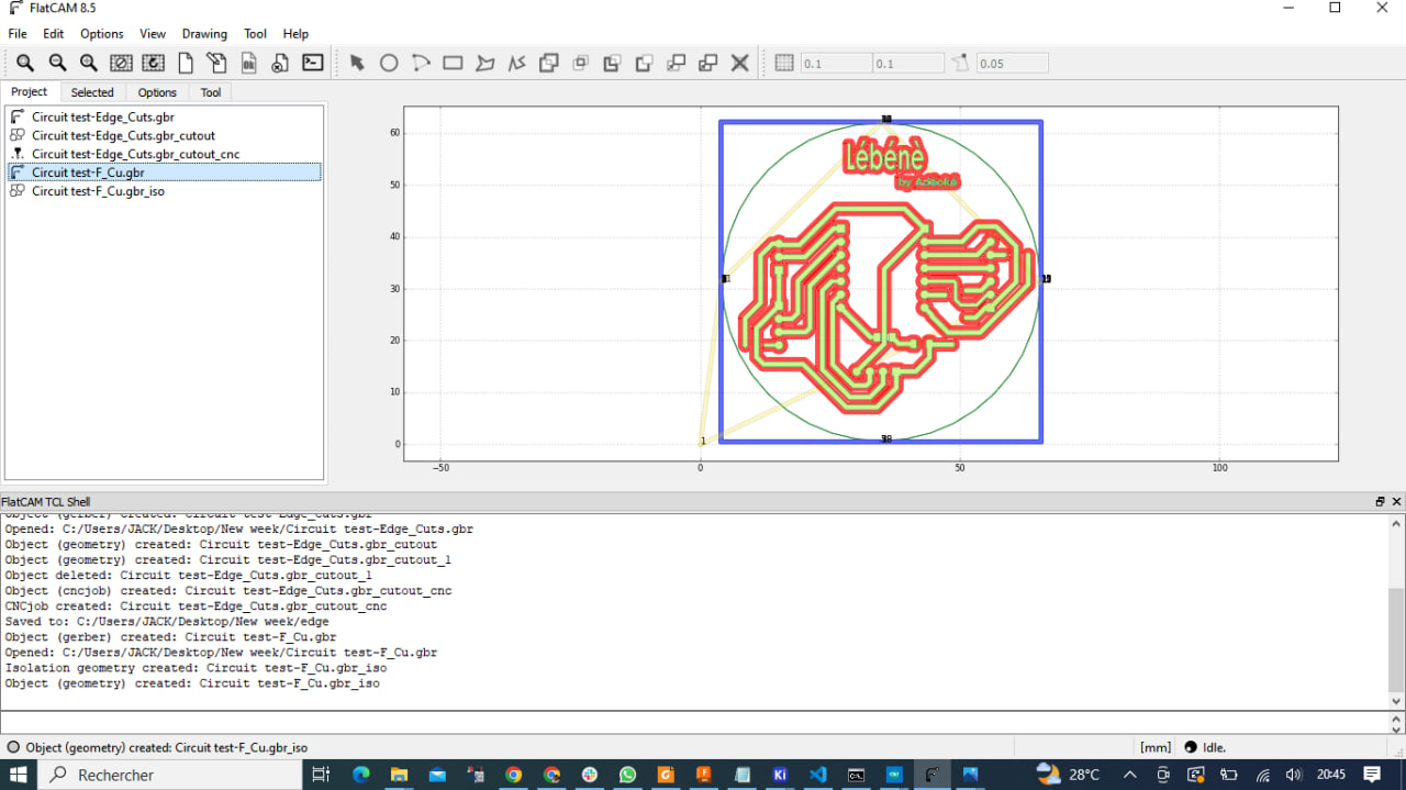
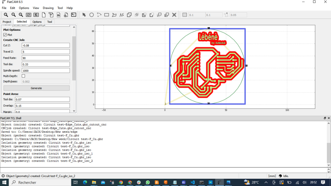
Here are the main parameters I used for “Font Cut”
| Parameter | Value |
|---|---|
| Cut Z | -0.08 mm |
| Travel Z | 5 mm |
| Feed rate | 90 mm/min |
| Tool diameter | 0.33 mm |
| Spindle speed | 1000 mm/min |
| Pass overlap | 0.5 mm |
Still using the same process, we generate the Gcode for making the holes.

Here are the main parameters I used for the “Hole”
| Parameter | Value |
|---|---|
| Cut Z | -1.6 mm |
| Travel Z | 5 mm |
| Feed rate | 90 mm/min |
| Tool diameter | 1 mm |
| Spindle speed | 1000 mm/min |
Step 2: Set up the machine and run the operation
Having generated the Gcode, let’s move on to production.
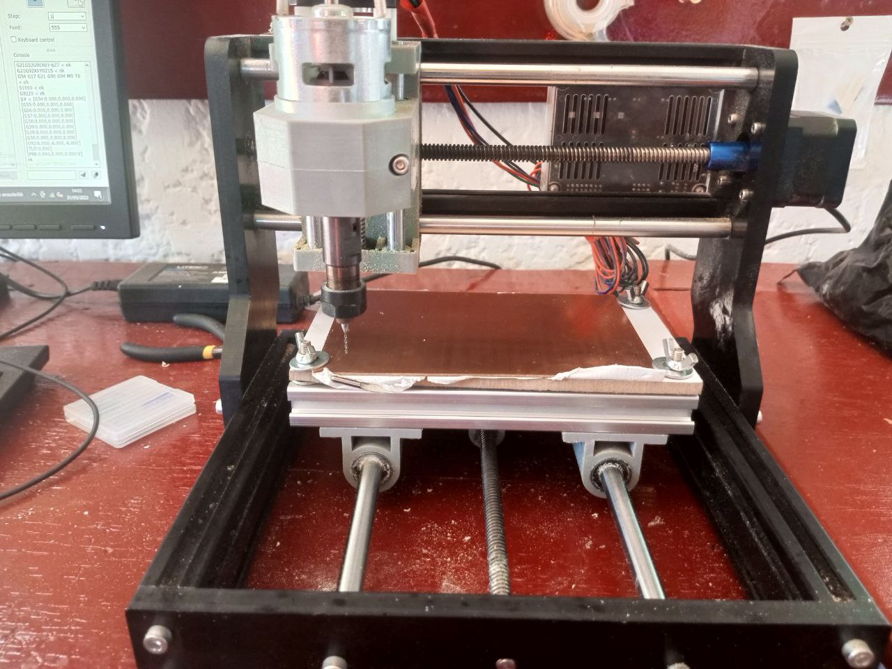
Here’s the cutting machine we have in our fablab.
Load file into software
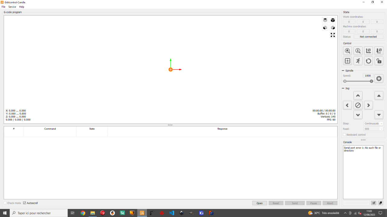
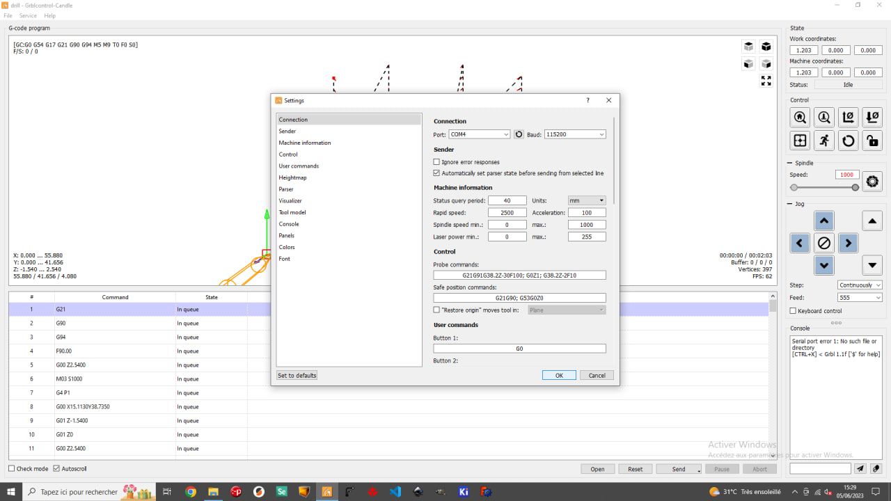
To control our machine, we use the “Grblcontrol-Candle” software, whose interface is shown below.
First, we load the Gcode for the holes into our CNC software.
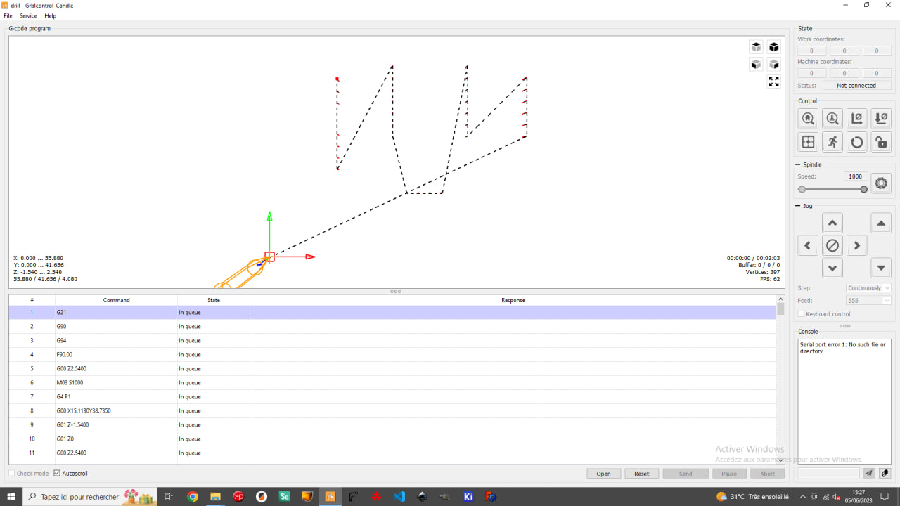
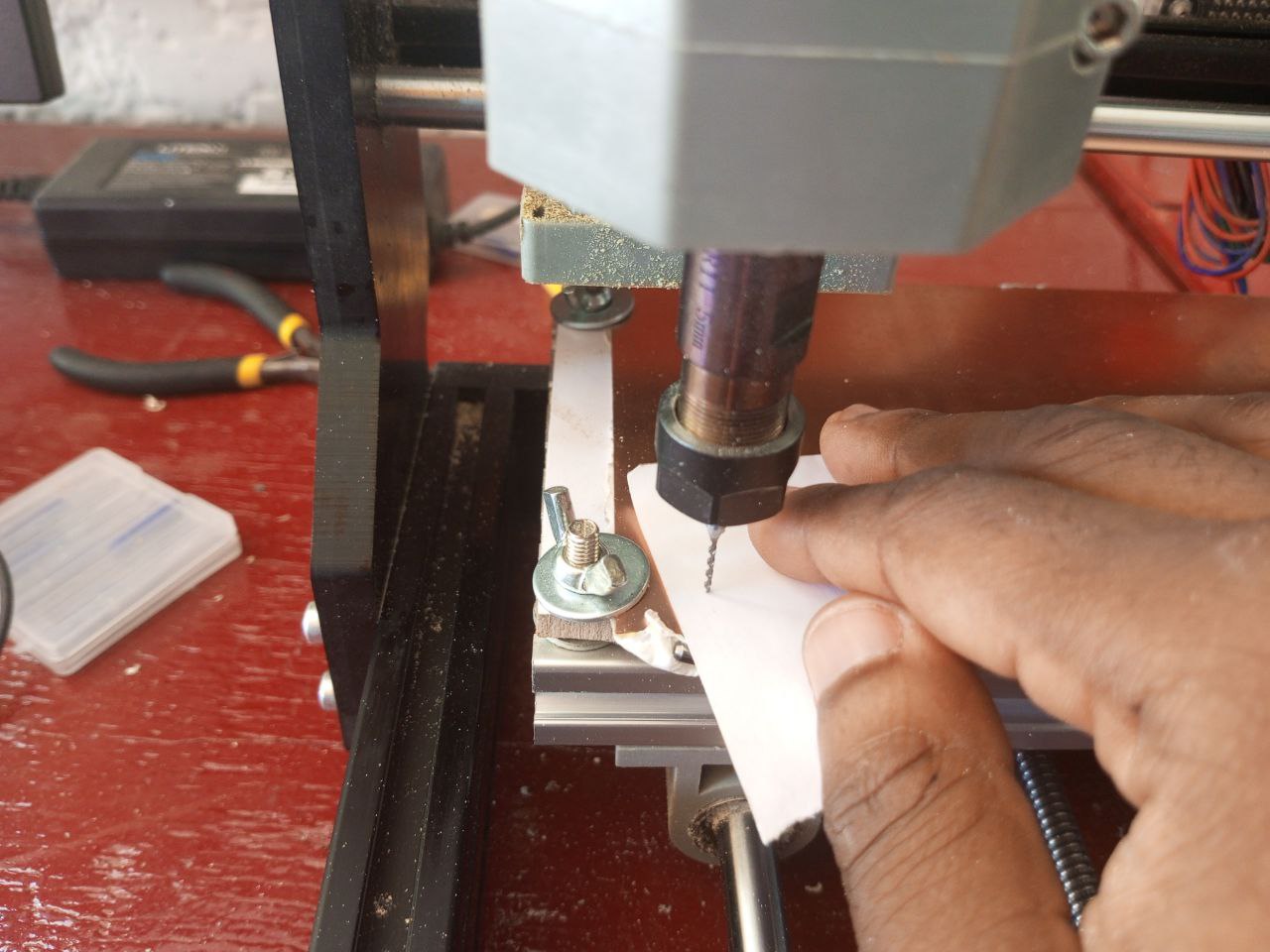
After loading the file, we need to check the various parameters to ensure that everything is correct. Then we launch the machine to make the holes.
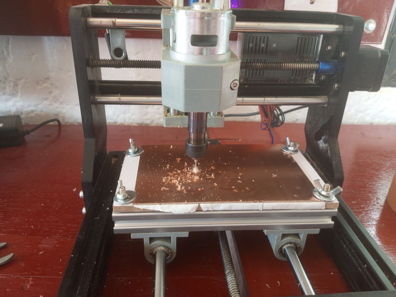
Once you’ve made the holes, load the Gcode to make the tracks.
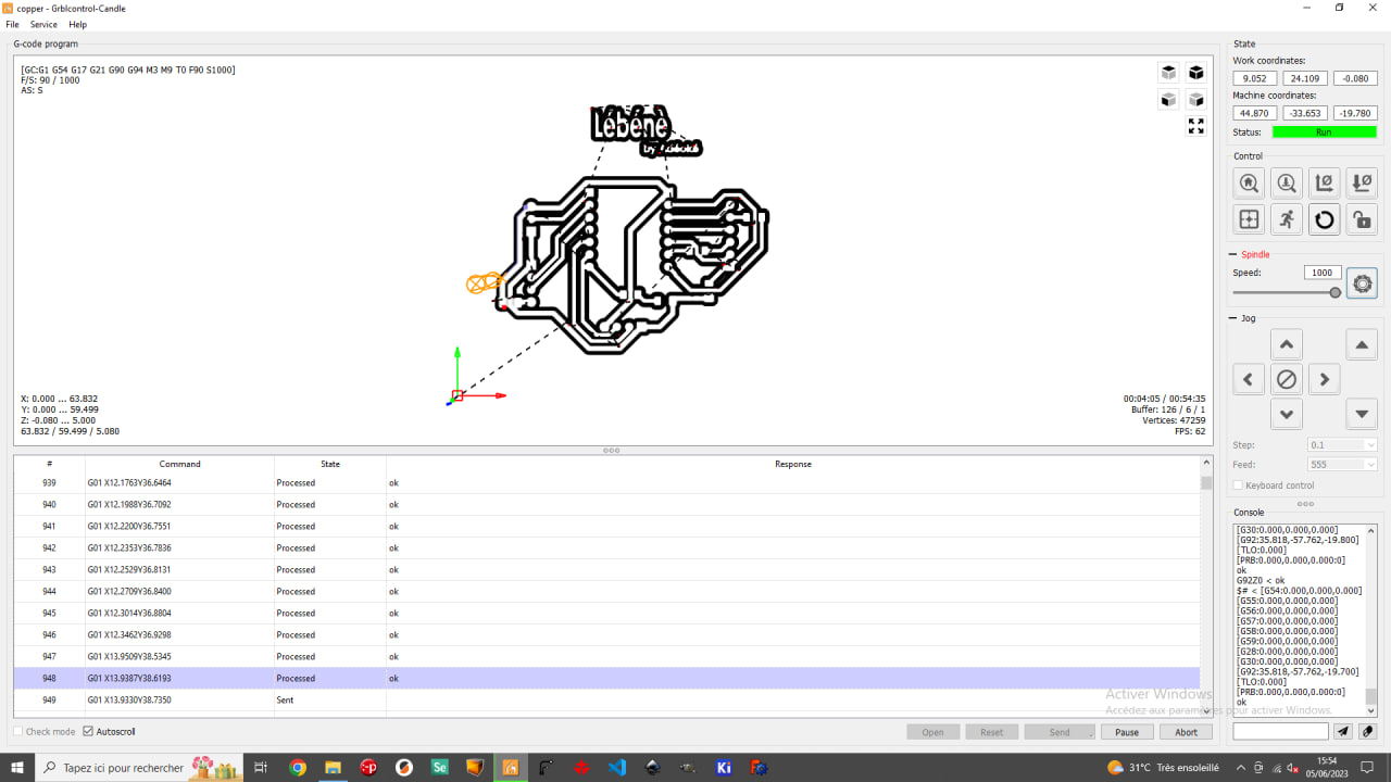
Next, we load the Gcode for cutting the shape, i.e. “Edge Cut”.
Install cutting material on machine and start CNC
First, we need to prepare the bed of our CNC to hold the copper plate to be cut. To do this, we use a double-sided skotch to hold the plate firmly on the bed.
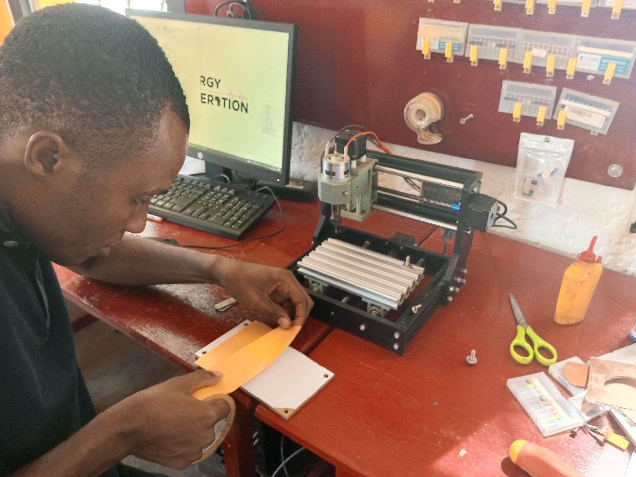
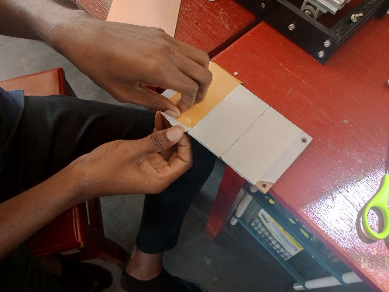
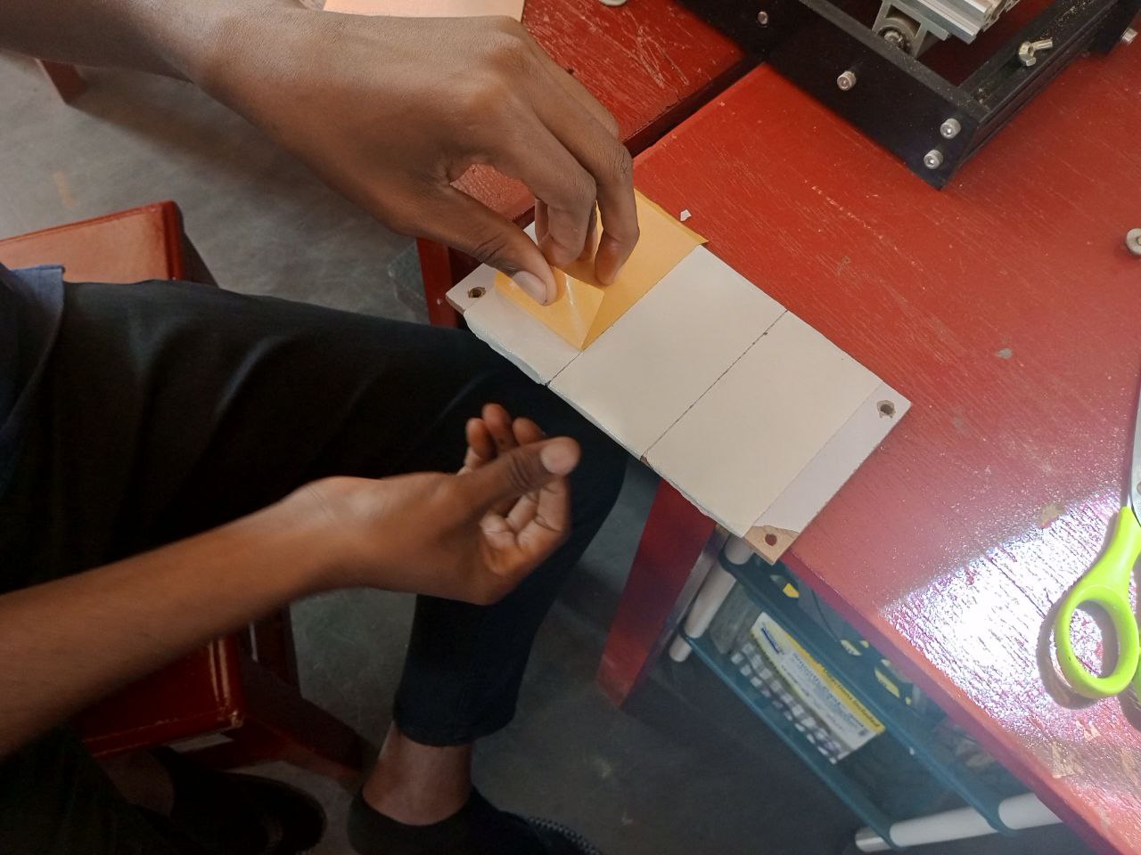
Now I place my copper plate on the bed
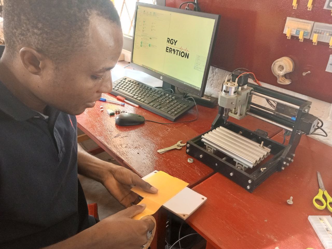
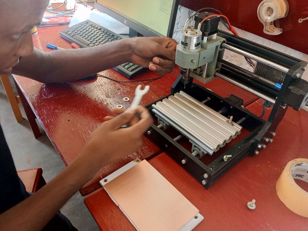
I change the machine bit
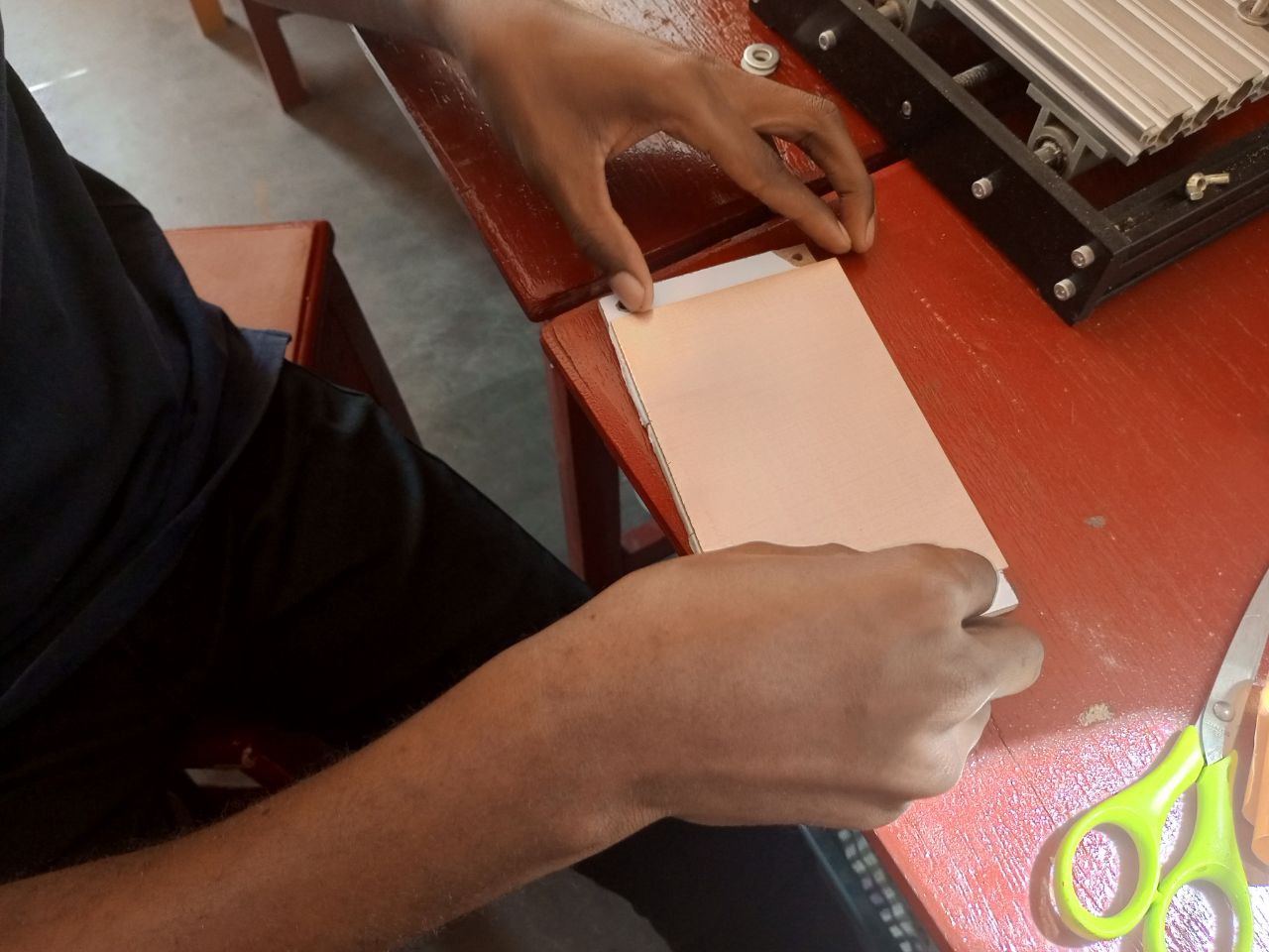
I check that my copper plate is correctly positioned on my bed.
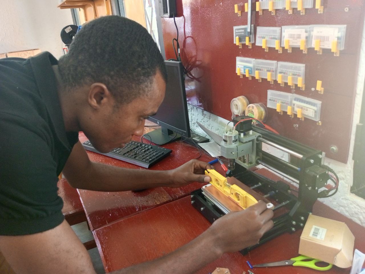
I set the origin
I launch the machine for cutting
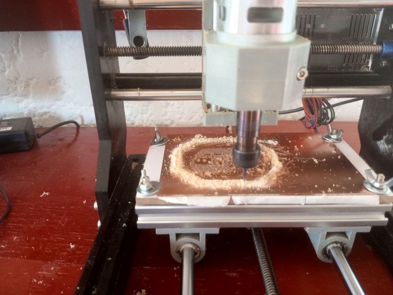
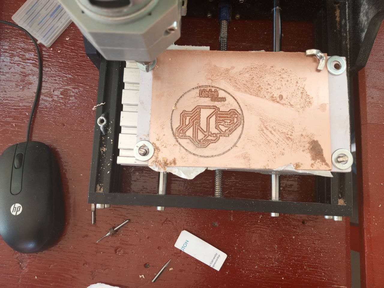
Step 3: Soldering and testing
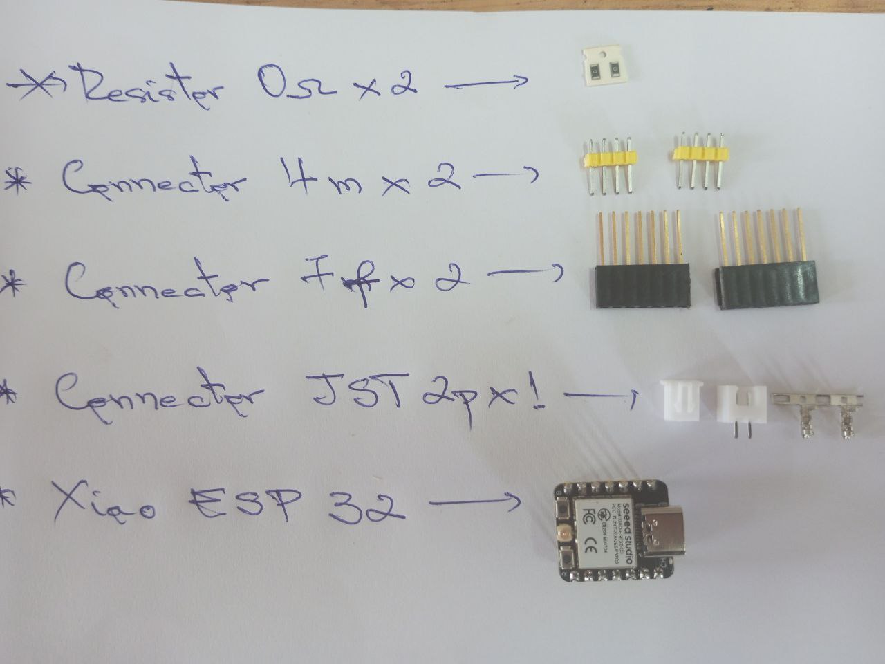
After cutting, let’s move on to soldering the electronic components onto my board.
To do this, I first made a list of these components.
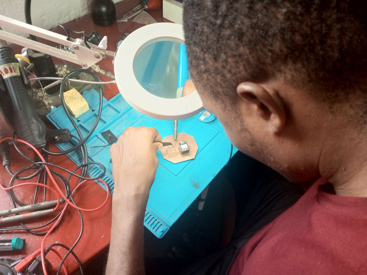
Then I started by soldering the components one after the other.
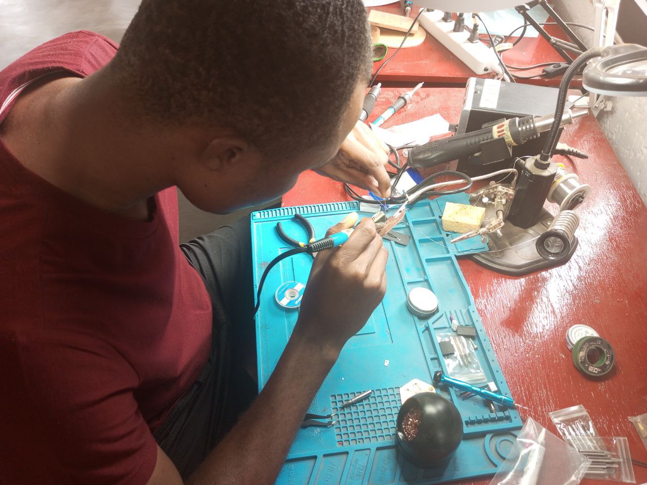
On this picture I used a soldering iron to solder the SMD components. I also had the option of using the reflow plate to do it, but I chose the soldering iron because it was easier for me.
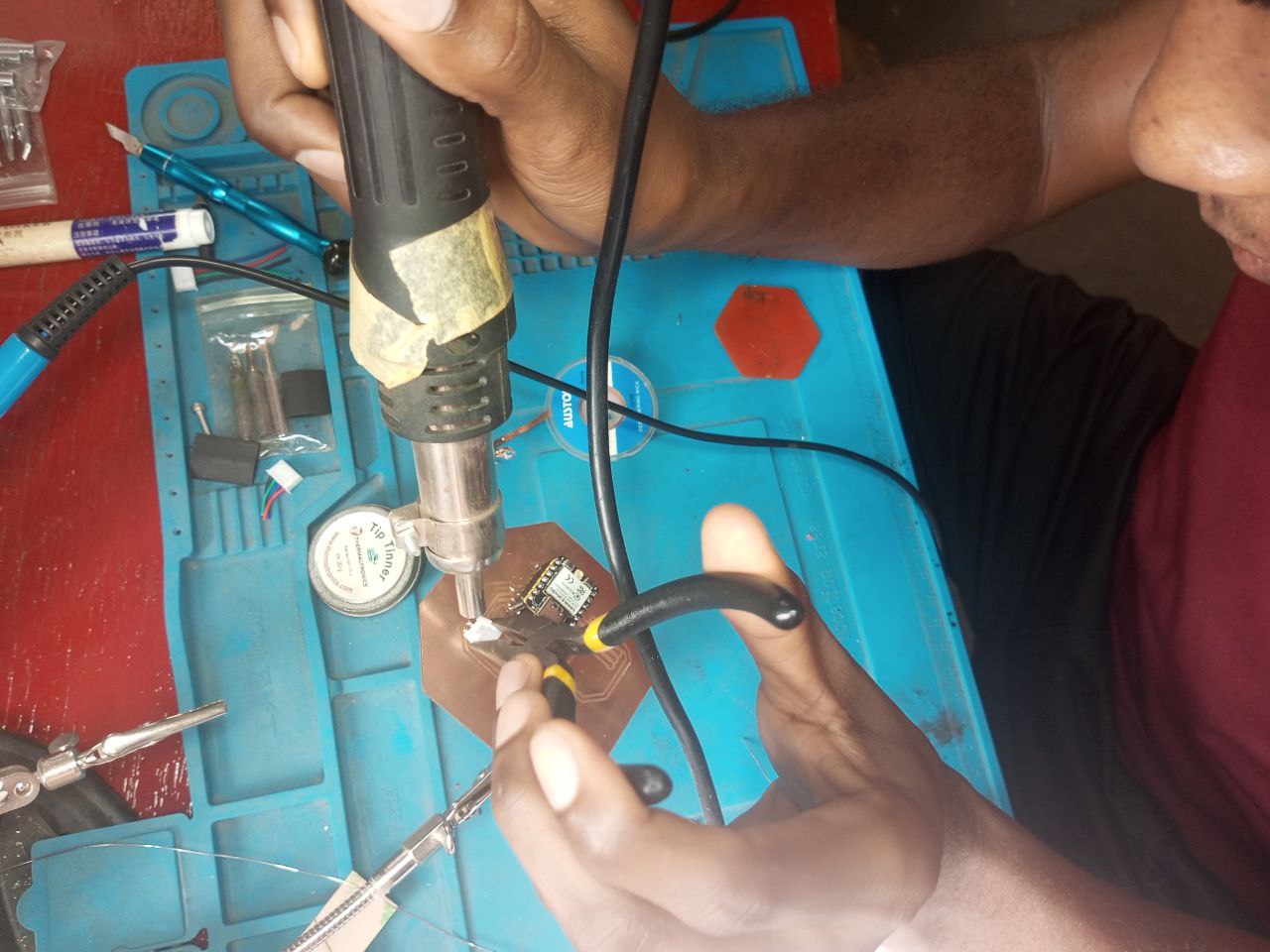
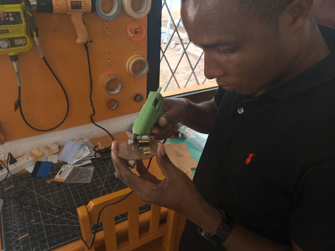
On this one I used the hot air gun to solder a JST component.
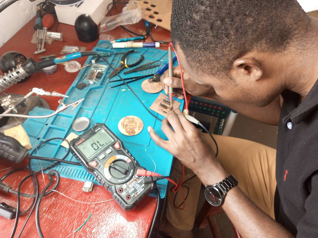
After soldering, I carried out some tests to check that everything was in order.
Step 4: Touch- ups
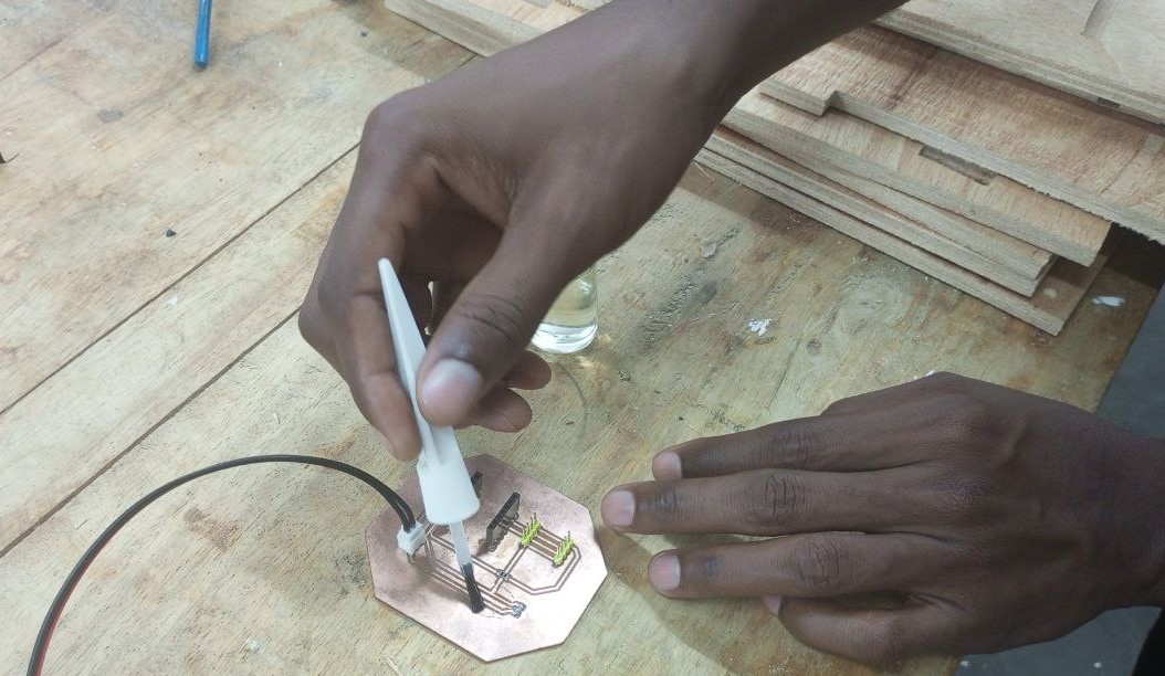
To protect my board against oxidation, I applied a little varnish.
I also used glue to solidify some pin components on my board.
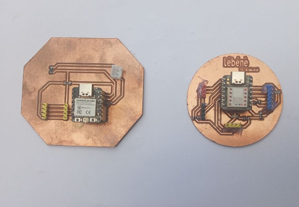
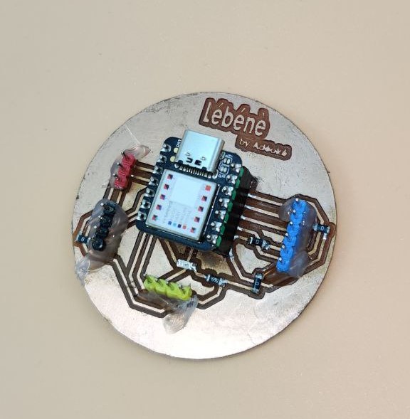
Final result
Here’s the result at the end of all these steps.
What went wrong / what went well
At the end of this week’s work, I can say I’ve learned a few new things, like soldering in different ways with different tools. It was a bit painful, but I learned a lot. What bothered me a bit was the soldering on the board, because the first one I did wasn’t any good and the board was no longer usable, as some of the tracks had broken off. So I had to reprint a new card before soldering again.
Files
The Kicad and Flatcam files that were created and used for this job can be found at the link below: