06. Electronics design
Hero Shots
Assignment Requirements
Group Assignment
Use the test equipment in your lab to observe the operation of a microcontroller circuit board (as a minimum, you should demonstrate the use of a multimeter and oscilloscope)
Document your work on the group work page and reflect what you learned on your individual page
Individaul assignment
Design a development board to interact and communicate with an embedded microcontroller
Group assignment
Requirements:
Use the test equipment in your lab to observe the operation of a microcontroller circuit board (as a minimum, you should demonstrate the use of a multimeter and oscilloscope)
Document your work on the group work page and reflect what you learned on your individual page
Link to group assignment page
You can find images and videos of all these tests on our fablab website by clicking here .
To test our board, we used the multimeter in its different modes: Voltmeter, Amperemeter and Continuity meter.
In continuity mode, we used it to check the insulation of tracks and plates in relation to each other, in order to avoid short-circuits.
To measure the output of the XIAO board, we used an oscilloscope to flash an LED.
it is also embedded directly in the webpage below.
Individual assignment
For this assignment I’ve decided to design a printed circuit board that I could use as much as possible for my final project. To do this, I need to learn how to use Kicad. There are several software packages available for PCB design, but I’ve chosen Kicad because it’s open source.
It’s a collection of several different programs that work together to help design a printed circuit board.
Step 1: Learning to use Kicad
To learn how to use Kicad, I followed a series of videos on youtube, in particular on this channel. Apart from that, I was helped by our instructor and other colleagues in our fablab who know their way around.
Step 2: Identifying the components I’ll need
Here I had to identify all the components that would make up my system.
Step 3: Schematic
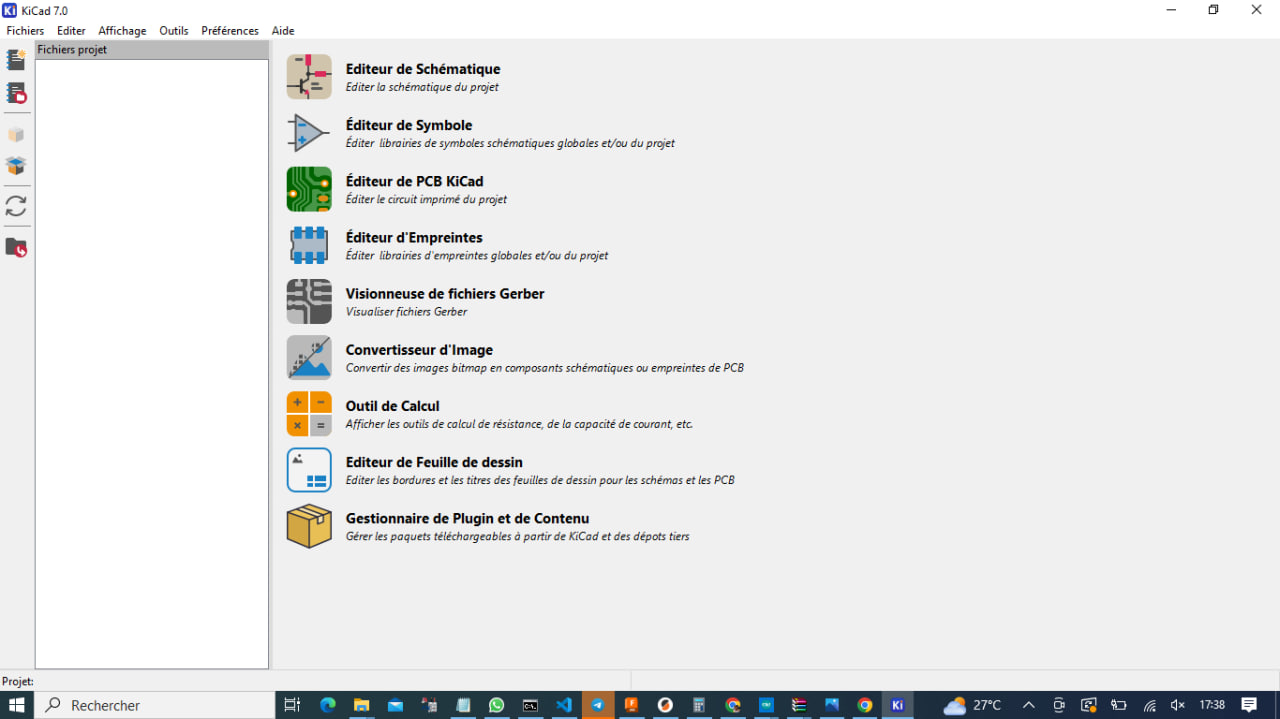
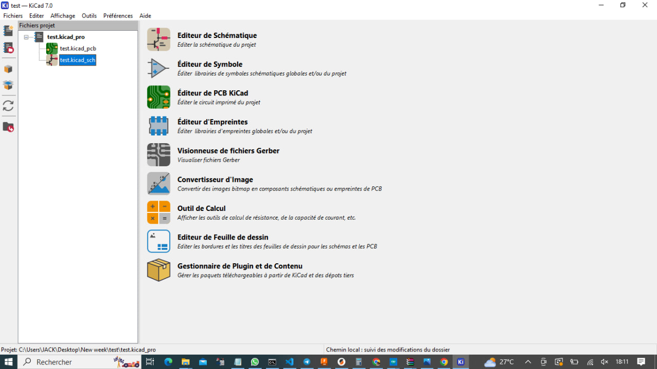
Having identified the components, let’s move on to the first step in KICAD, which is the construction of the schematic. To do this, we open Kicad and create a new project.
Then this window appears
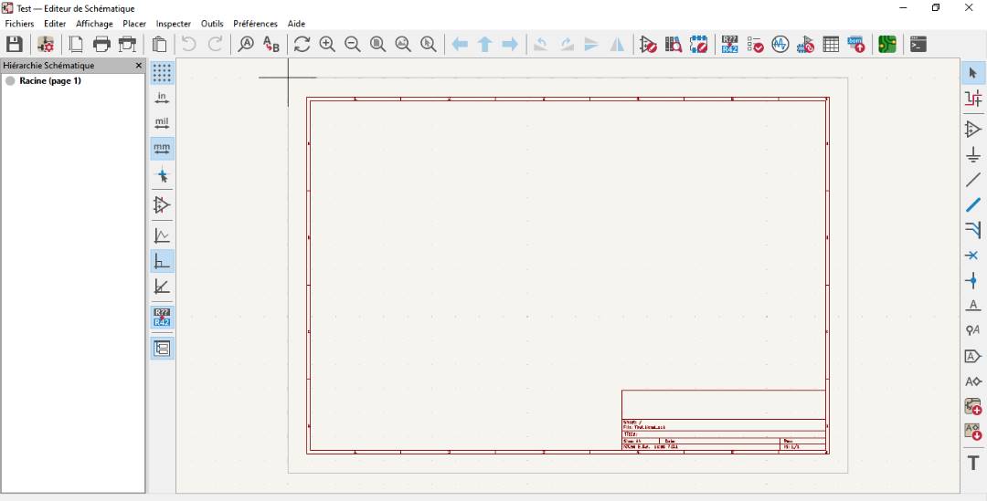
Double click on the schematic symbol
This window opens
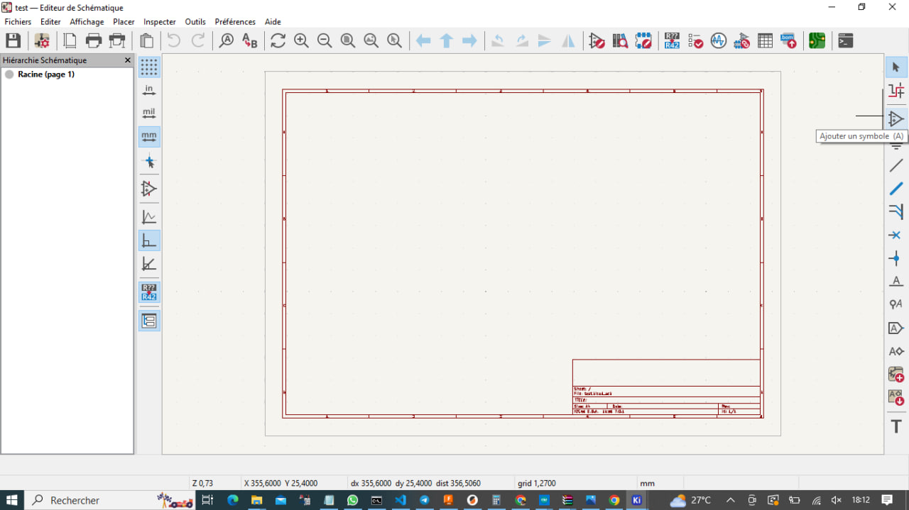
Now, to choose our components, we’ll select the symbol below by clicking on it in our window.

After selecting this symbol, left-click with our mouse and a new window will appear as below.
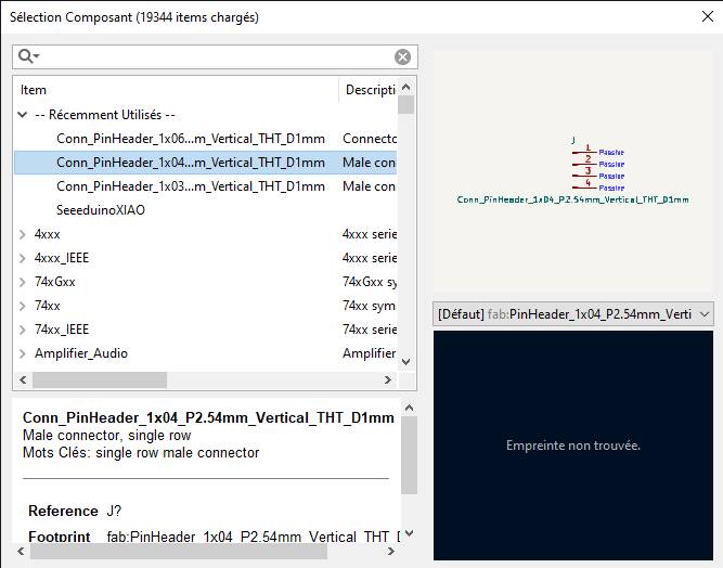
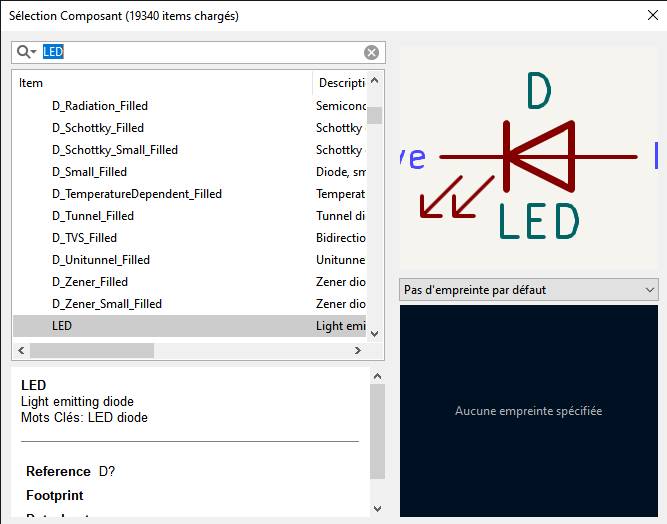
In this window, we can now select our components by doing a search as in the image below, on which I’ve selected an LED.
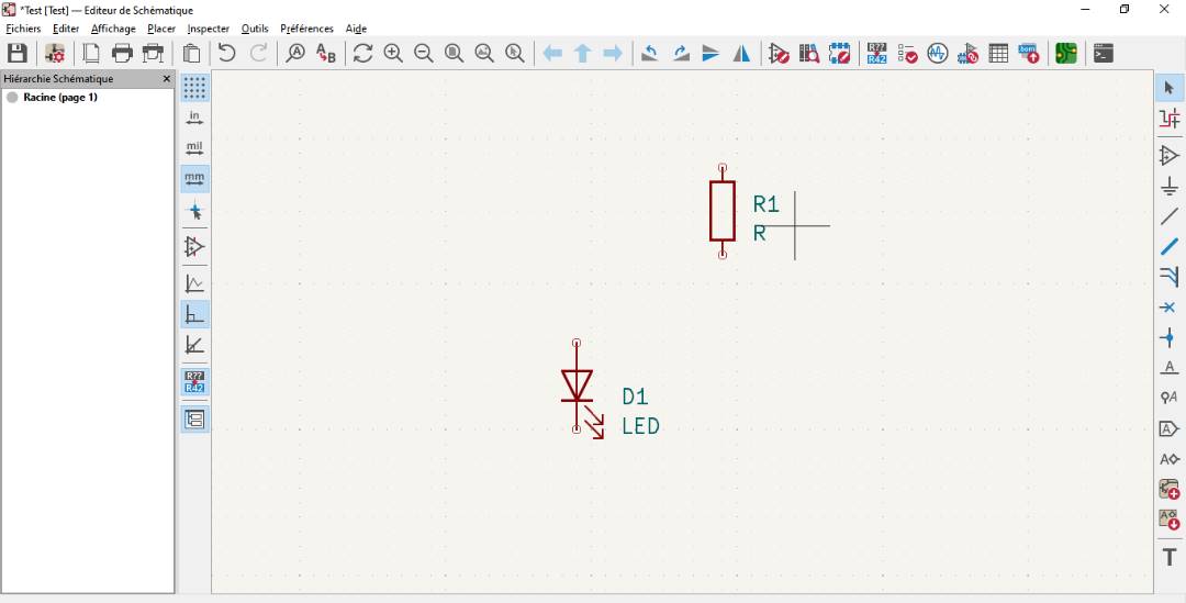
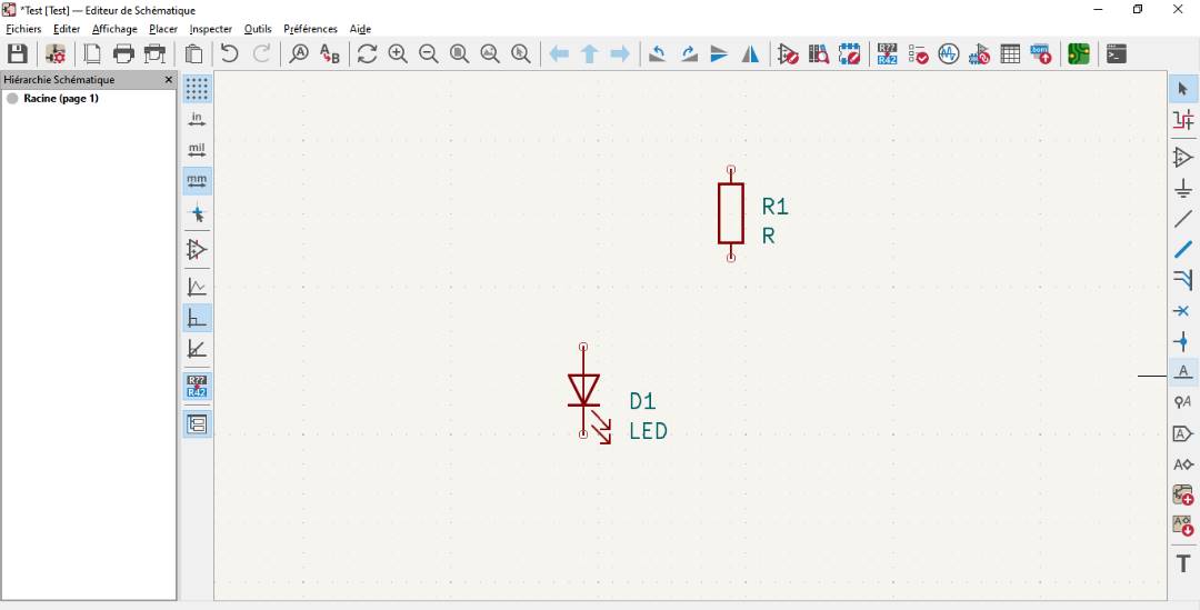
At first, I’ve just selected a resistor and an LED as shown in the image below, to demonstrate how these 2 components can be connected.
To connect these 2 components, you can either use the wires or the “LABEL”.
- Wire connection
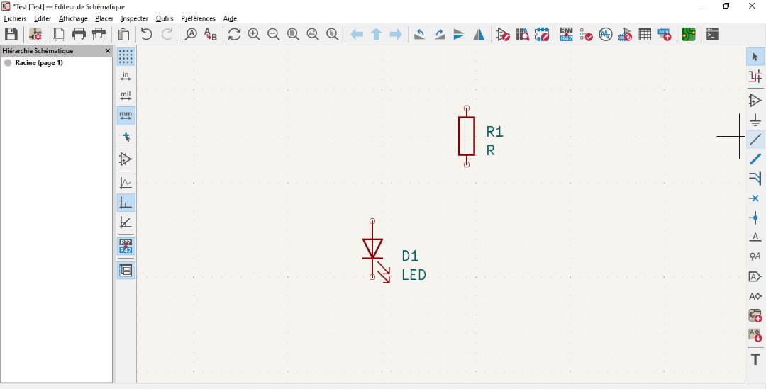
First select the “wire” tool from the toolbar on the right of the window, as shown in the image below.
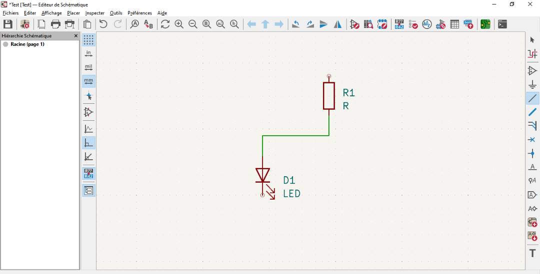
Then draw a line between the 2 components to connect them.
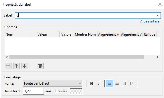
- Label connection To do this, click on the tool marked A with a line under it in the toolbar on the left, as shown in the image below.
Once you’ve clicked on it, a new window will appear in which we’ll give our label a name. In my case, I’ve named it “L”.
Then click on the ends of the components you want to connect, as shown in the image below, and you’ll see the name you’ve given your label.
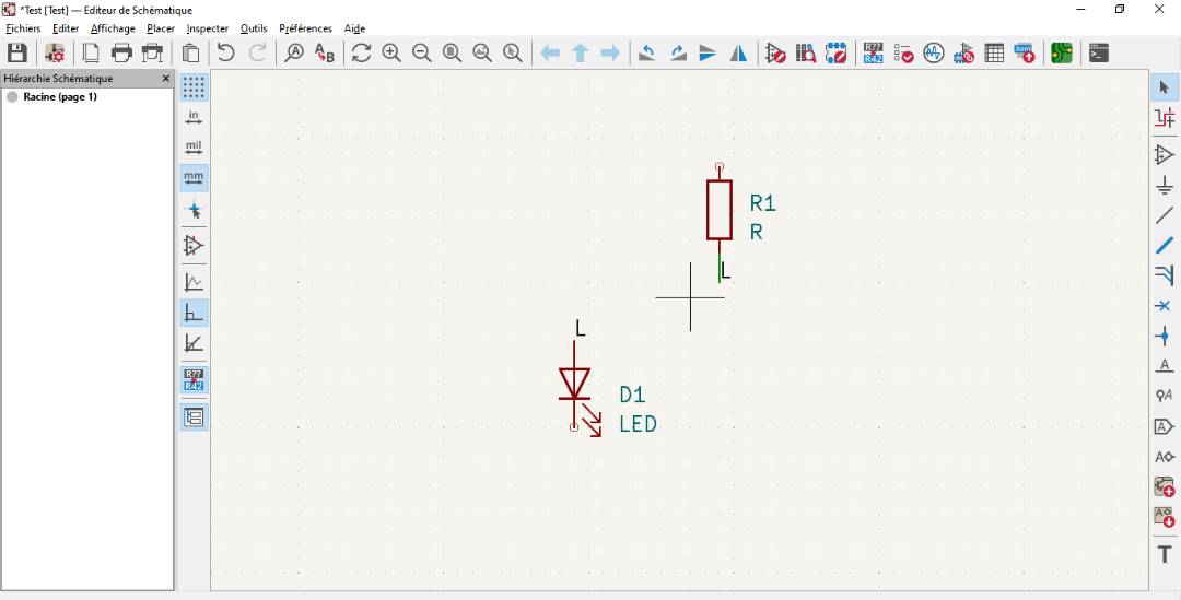
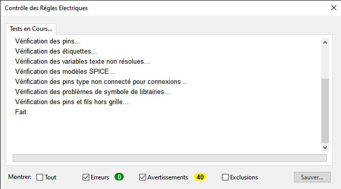
This is how, by selecting and connecting my various components, I obtained the result shown below.
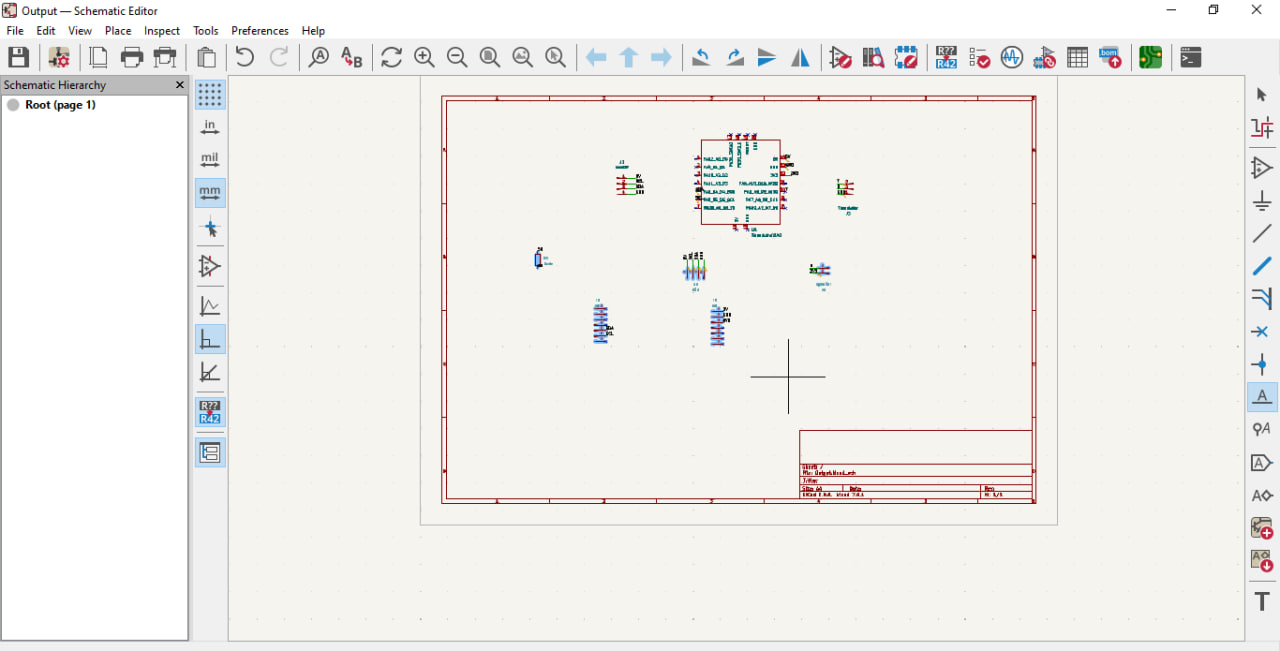
To finish with the schematic and go on to the PCB, we need to carry out an electrical test to make sure the various components are properly connected.
Step 4: PCB
After the schematic, we move on to the PCB. To do this, simply click on the icon below in your workspace, i.e. the window in which you created the schematic.

A new window will then open, as shown below.
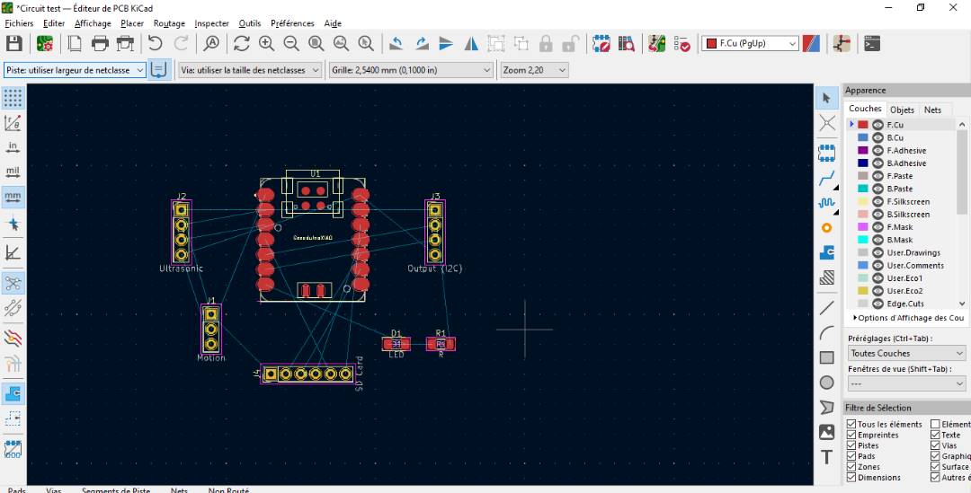
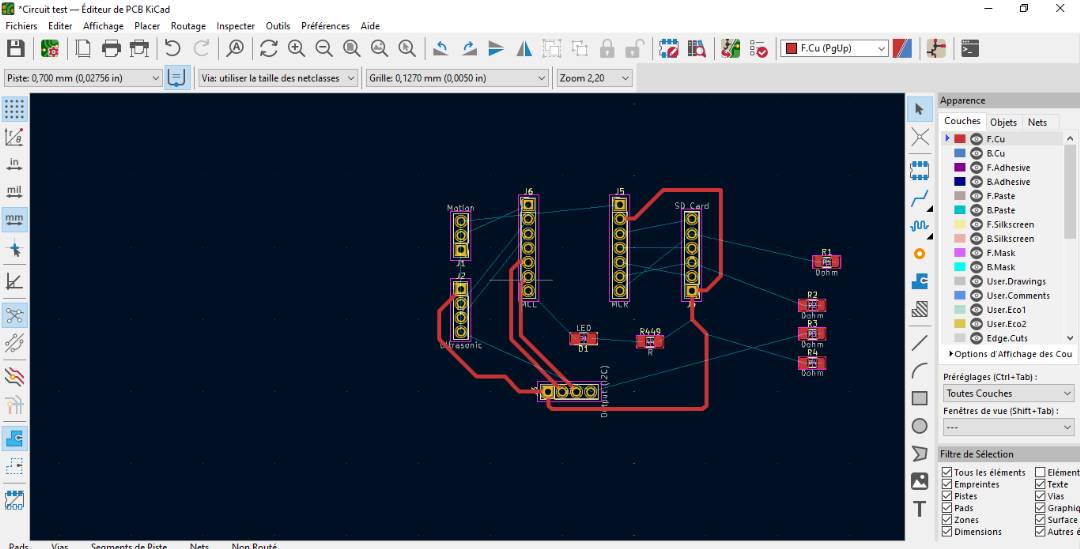
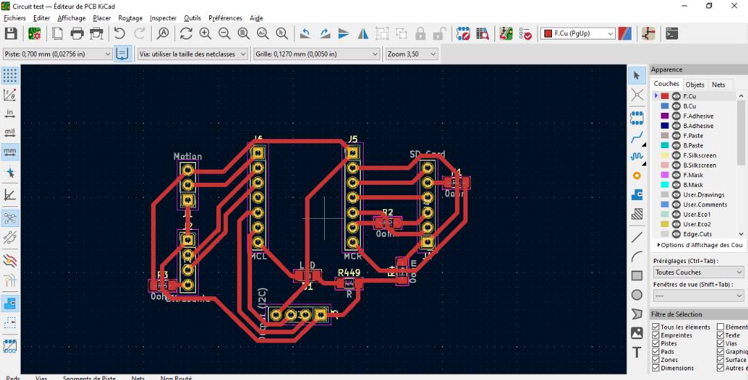
With the help of the little lines that can be seen on the schematic, we’ll be able to draw the different tracks that connect the pins of my components.
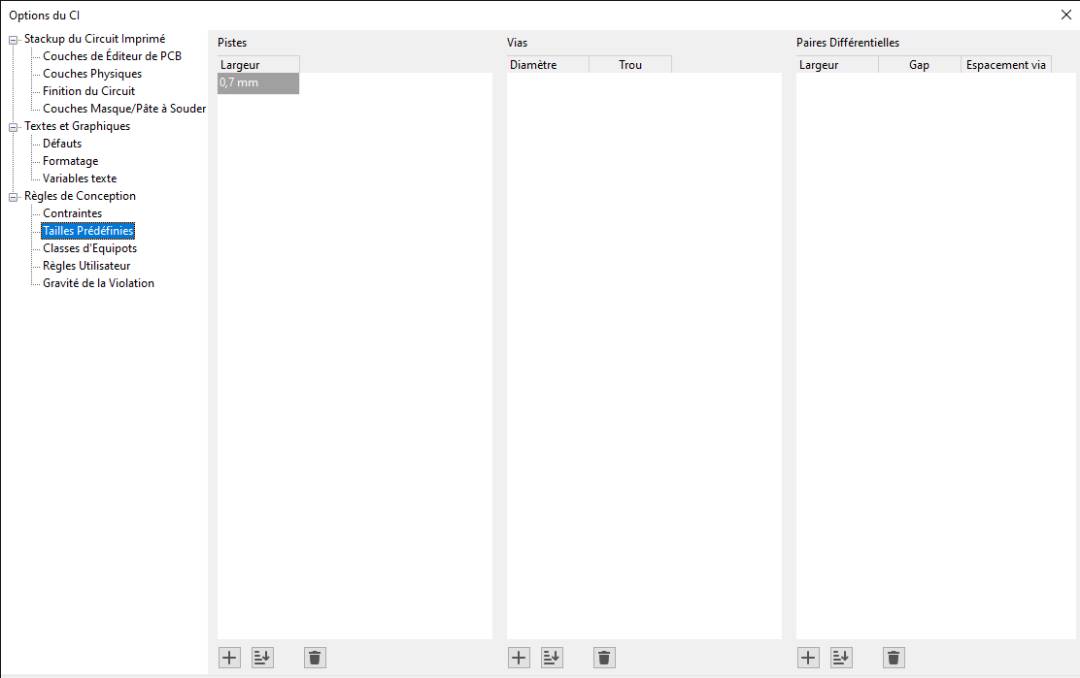
But first we need to choose the size of our track. In my case, I’ve chosen a width of 7 mm.
After validating the track width, we can now draw the different tracks.
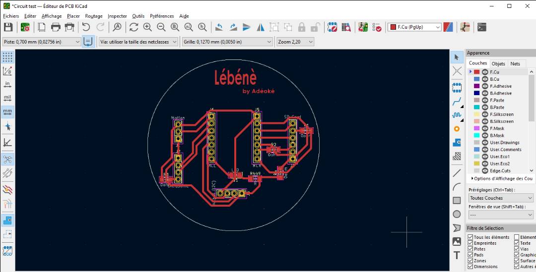
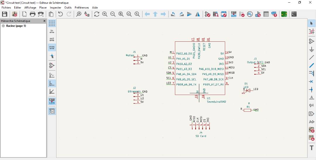
I had to design 2 boards, and here’s the schematic below.
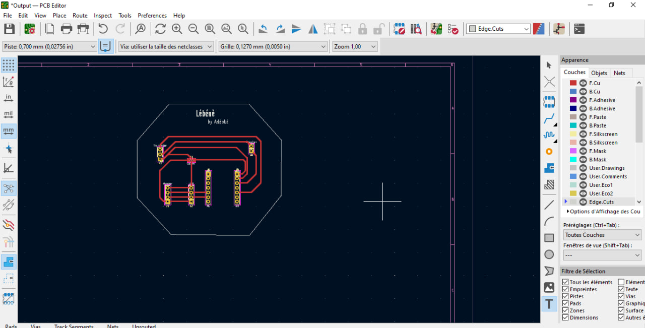
After tracing the different tracks, we’re going to delimit our PCB. To do this, select “Edge Cut” in the window and then draw the shape you want. You can also write text on your PCB. For example, give your PCB a name. In my case, I gave a round shape to one of my PCBs and a hexagonal shape to the second, then wrote a name on it, as shown in the image below.
- What this board does:
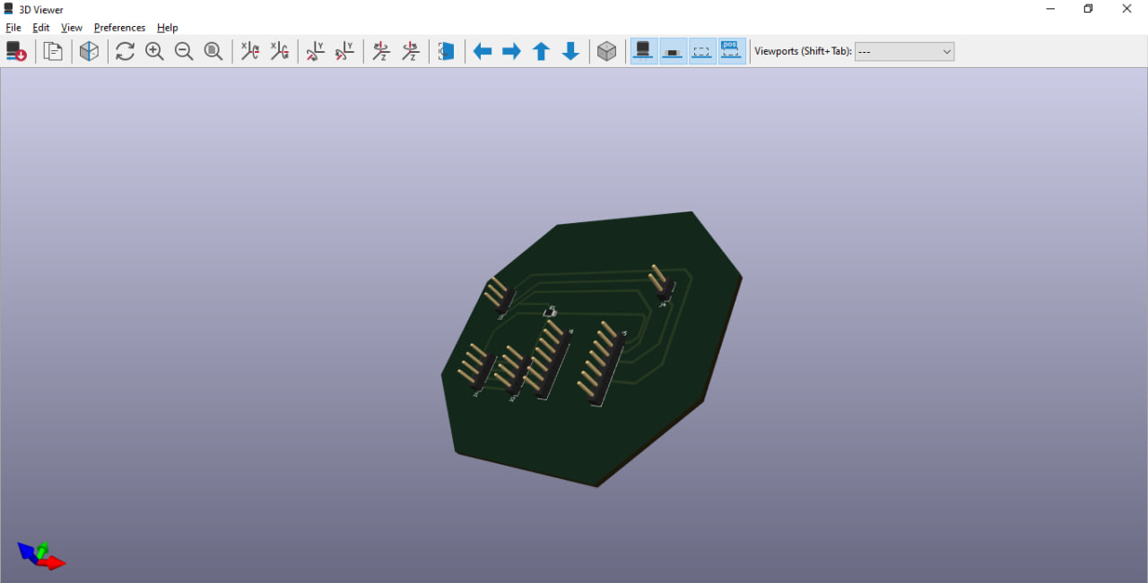
This board is the input device board for my final project. On it, a XIAO SAMD21 microcontroller is connected to an ultrasonic sensor, a motion detector, an SD card and an output for I2C communication with the second board, which is the output devices.
- Its purpose:
Its purpose is to collect data from its various sensors and process them in order to send a signal to the output devices board for execution of a specific task.
- What this board does:
This board is the output device board for my final project. A XIAO ESP32C3 microcontroller will be connected to it, along with an LCD screen, a small speaker and an output for I2C communication with the first board, which is the input device board.
- Its purpose:
Its purpose is to receive signals from the input device board and execute them, displaying messages on the LCD screen and emitting sound through the loudspeaker.
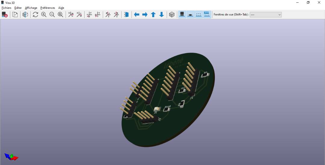
You can also have a 3D preview of your PCB as shown below.
Step5 : Export
Once you’ve created your PCB, you need to export it so that you can use it for cutting. In the export process, you need to select the various operations to be carried out by the cutting machine. In my case, I’ve only selected 2 operations (F.Cu and Edge Cut) at this stage, as shown in the image below.
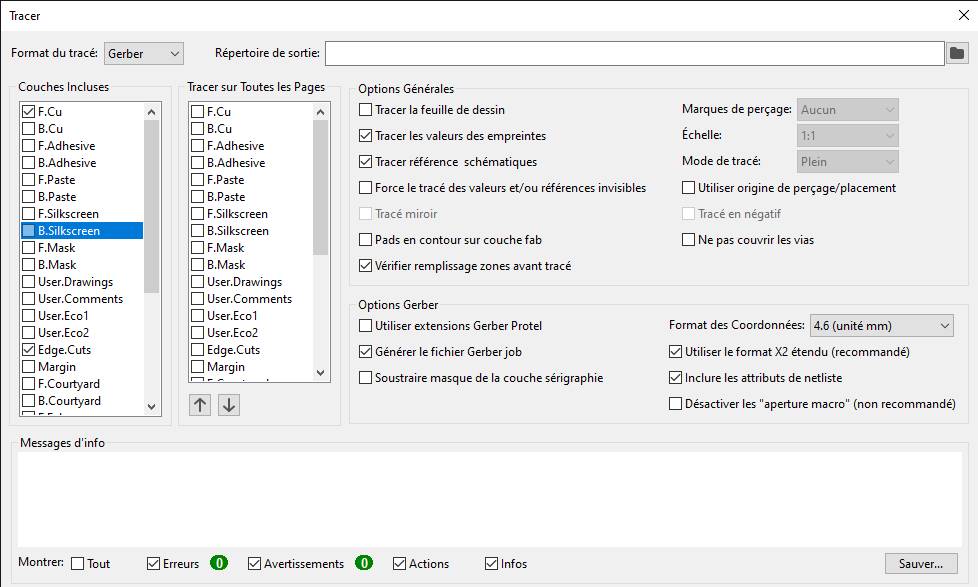
Then you can export in “GBRL” format for further processing.
For the rest, see you in week 8 for production.
What went wrong / what went well
During the design phase, everything went smoothly, but I did encounter a few difficulties, such as the footprint of certain components that were not directly visible in my Kicad. I had to do some additional research to find them. This was a bit constraining but it allowed me to learn even more.
Files
The files that were created for this assignment can be found at the following links: