Week 08

Electronic Production

This week is about fabricating the board that we have previously design two weeks ago. Then, learn how to solder all of the components and programming it to have communication with the computer.

  • Week 14th - to 21th of march
  • Keywords SRM-20, endmill, pcb
  • Software Kicad, Modsproject
  • Group assigment
  • Here

01PCB

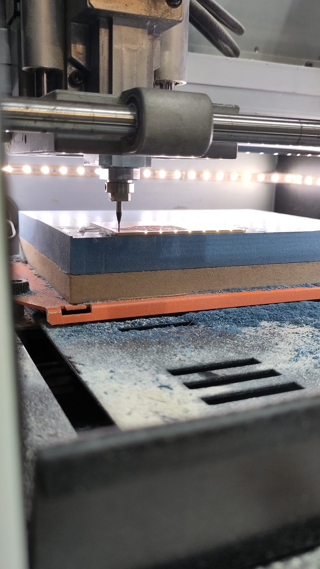
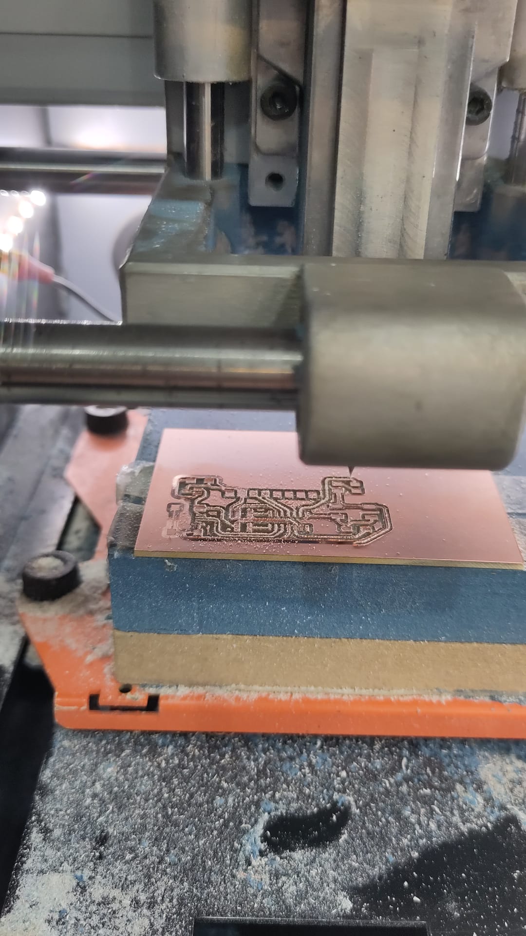
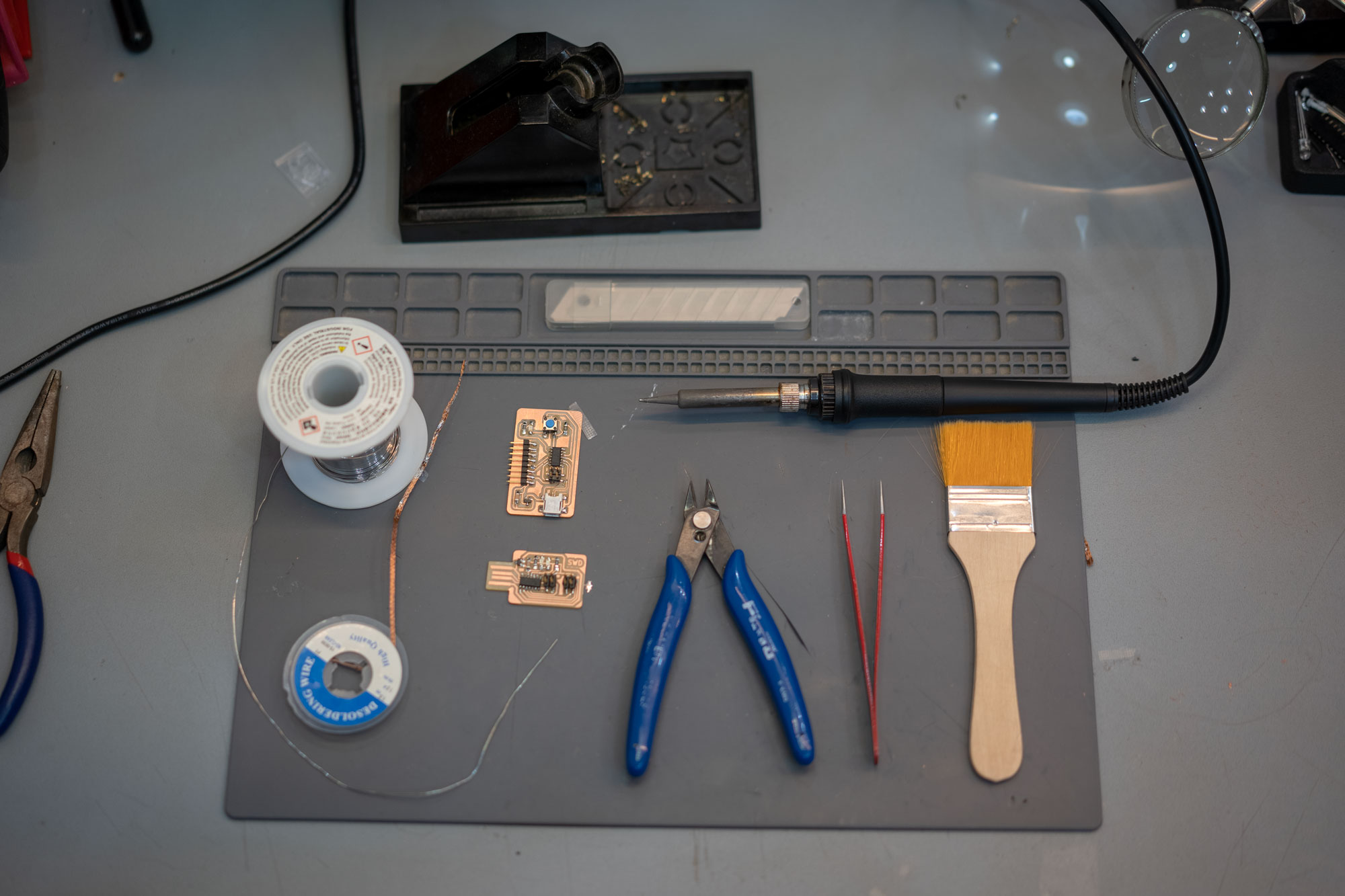
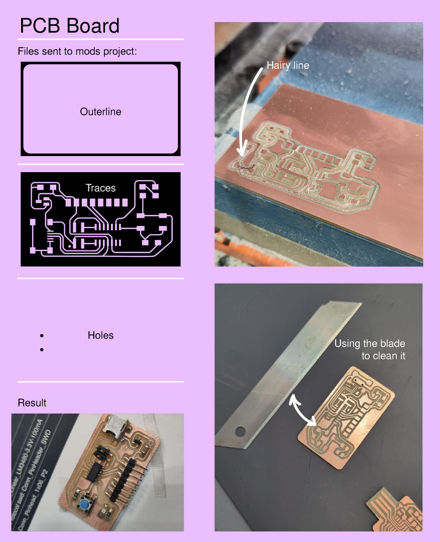
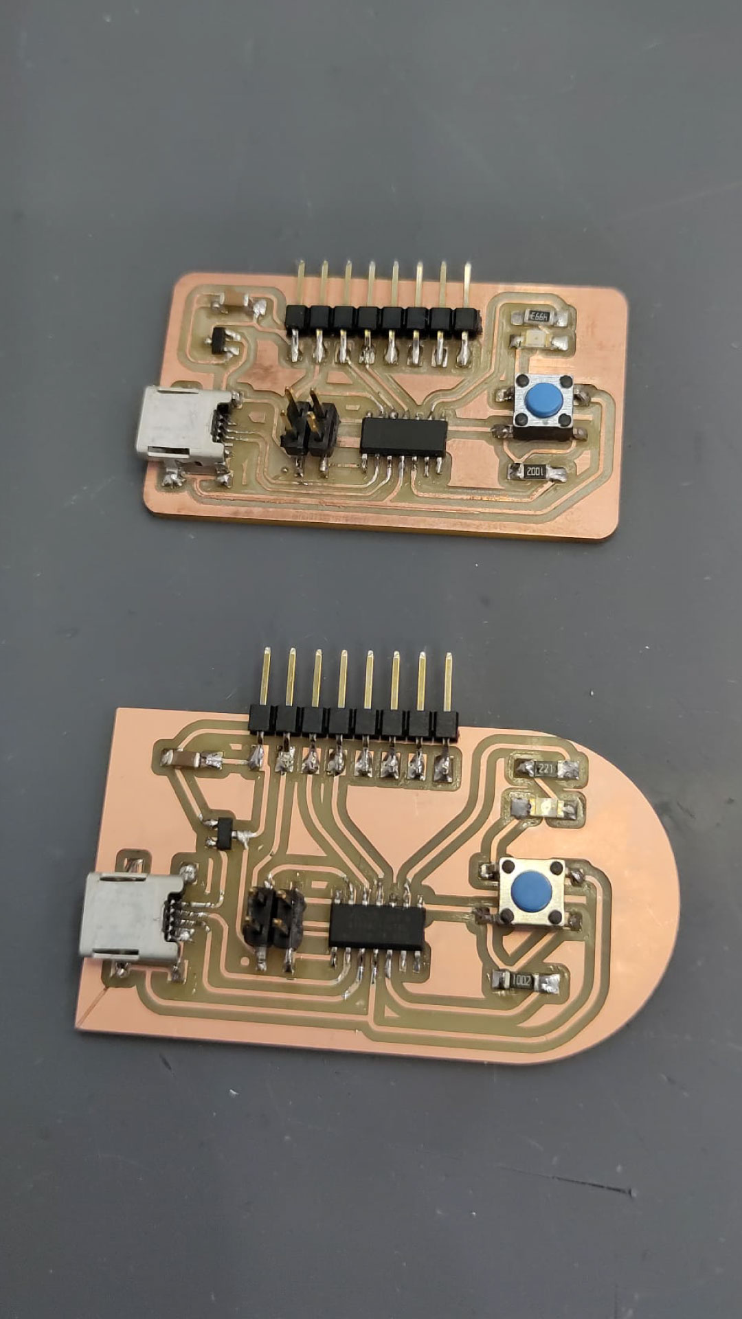
PCB printed circuit board, there are many types and process on how to produce them like with acid, cnc milling or cut it in the vinyl cutter.
The ones that we will be using are FR1: this mean the material inside the coper is phenolic resin. It is standard the amount of thickness through all the boards.
Design Rules: The distance between the traces needs to be at least the size of the end mill. We are using two different ones. 1. 1/64 inch (0.4mm) for doing traces * This is why in kicad, we were designing considering the clearance of the end mill. 2. 1/32 inch (0.8mm) for the holes and outlines.


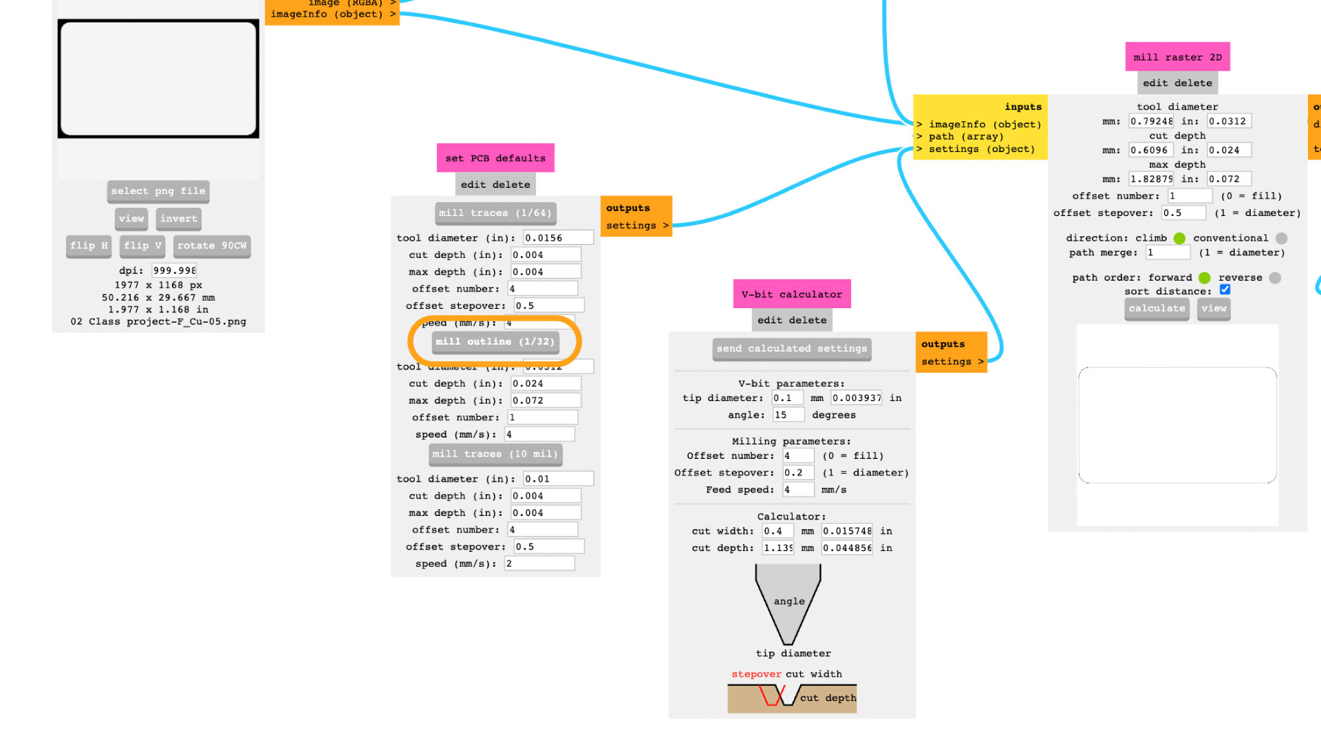
Prepare the files from kicad and Mods


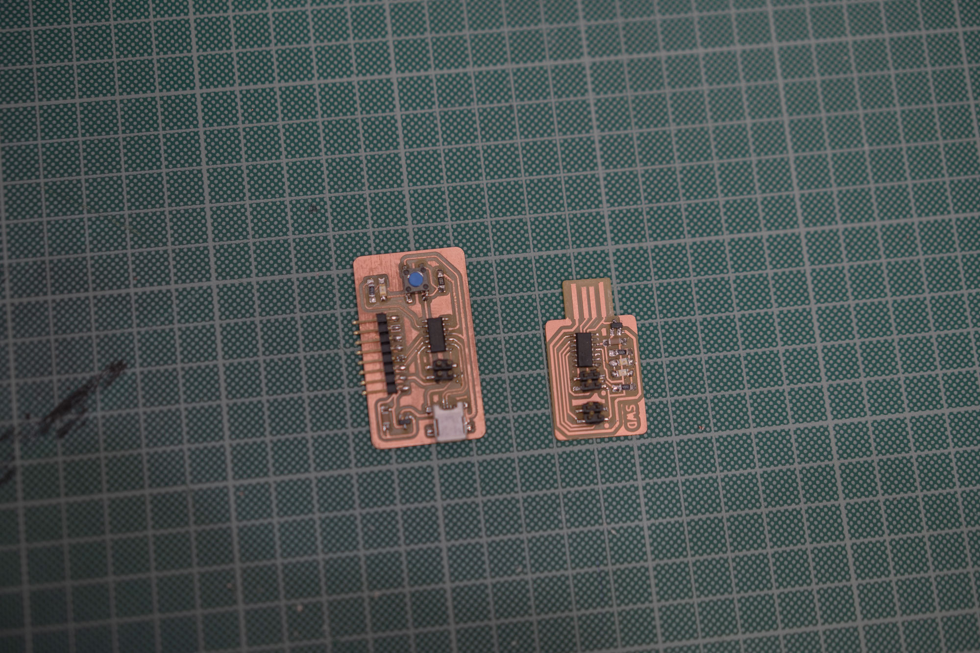
1. We need to export as SVG from the PCB Editor in kicad, then a pop up window comes and we need to choose what to export, in this case the copper layer, the edge cuts, black and white for print mode and the board area only for the svg page size.

2. Export to illustrator as the svg to divide the files into inner lines, holes and outer cut. Whatever is in white we are going to keep it and whatever is in black gets cut.In the case of the inner lines I added more radius to the corners so it will look more smooth.

3. Mods to export the files for the SMR-20
  • Open program
  • Choose in Rolland SRM-20 Mill PCB
  • Upload png file with 1000dpi
  • Set PCB defaults, choose the mill trace necessary
  • Mill Raster 2d: In offset number 4 its nice, in case of wanting to clear the copper we can put 0 and direction climb is fine.
  • Define setting of the machine, Speed 3mm, the origin needs to be always 0 in X Y Z not to create any offset. Jog height: 5mm
  • Turn off setting directly to the machine and on to download the file
  • Select Calculate to see if it works.

  • In the photo 01, we can see how to set up 0 to the axis, becuase the endmill specially the 1/64 its so delicate its better to loss a bit the end mill and let it touch the material, that way the Z would be exactly on the place without pressing on the tool.

    02SRM-20 TUTORIAL


    1. Prepare the components
    Take the copper board and put two stripes off double side tape longer than the board, not overlapping the tape in order to have a flat surface.

    2. Turn on the machine
    On the top right corner we turn on the machine, then open V-Panel that is the software to cut the files

    3. Fix the PCB
    Align to the left down corner to press it down the surface.

    4. Lead the end mill
    First using the 1/64 end mill for doing the traces we need to open the collet with an Allen key and introduce it slowly

    5. X Y Z
    First move with continuous move the X and Y to the left corner and then small step movements for the Z with the x10. Leaving it 3mm distance from the pub board and then with the collet we lower that amount gently to touch the pub board.

    6. Prepare the files
    As I explain more in depth above, we are using Modsproject but here is how was describe in the tutorial as a faster approach.
  • Add the png files: One for traces or inner lines, one for holes and one for outer line.
  • Check that the Dpi its 1000px and the size of the board is correct in mm
  • Choose the process: Mill traces 1/64 or 1/32 depending on the file.
  • Change the speed of the machine (1/64 it would be 3 or 4 and for the 1/32 would be 0.5mm per second ) and not having any offset so the origin point needs to go to, so we need to change it to 0 and check if the jog height is 2 mm( means how high the machine is going to move in the air)
  • Check in Calculate and save automatically the file


    7. Cut!
    Choose the file, added to the V panel software and once press output to start automatically start producing it. This process needs to be down twice, the first one to use 1/64 for the traces, stop the machine, changing the tool for the 1/32 (always reset the parameters of X, Y, Z and then cutting holes and outlines.


    Possible Mistakes to be aware off when doing this process:
    Bad Z offset
    Too high it will scratch the copper leaving a shinny surface but not taking out all of the material.
    Too low is going to look hairy, this might not be a problem because it can be sanded with iron paper or iron wool to clean it.


    03Milling and soldering my PCB


    01 Milling

    I started with the inner lines and using the 1/64 end mill, it was really easy to put inside the collet, kind of adding a new needle in a sewing machine. Then, after adding the files, in the first 10 seconds I realise that the end mill was scratching the copper but leaving a shinny look, this means the end mill was not going deep enough and I stop the machine, with the collet put it a bit lower and start again the file, It cut about 15 minutes until the end mill broke :( I had to change the broken end mill and add a new one, we checked with help and it could have being a used end mill or was not completely flat from the surface. After reloading the file, the first part I adjusted the speed to 40% until it reach the point the need to cut from 0 and speed it up 60%, I wasn’t in a rush and didn’t wanted to break another tool, so I send it to this speed.

    Once it was done, I changed the end mill to the 1/32 that is clearly more resistant, added the holes file, which took less than 5 seconds, then the outer line file.

    When it was done, took the brush to clean the copper power and check if it cut through, unattached the tape from the sacrificial board and then I checked that on the part that the end mill broke the line is hairy, only in that side of the board, so I had to take some iron wool and scratch those detials.

    02 Fining the components

    This was a task that took longer than expected. A lot of the reference in the drawer of the lab space are written different than in kicad, so the easiest was to go paciently, checking in google how they should look and then opening drawers, confirming with collegs.
    But suuuuper important it was before starting, having a clear list of the things we needed, masking tape to attatch them to a paper and taking photo of the drawer that it came from.

    03 Soldering


    For soldering, as a general recommendation, it is always better to start from the inner and smaller components to the outer lines. By adding a bit of melted tip on the trace of copper and then trying to attach the legs of the component * Even the side of it. Being careful that some of them needs to be done by specific side.
    Be super careful that there are not super small pieces of copper connecting lines, could do a shortage.

    In my case, there was two boards to solder one for the programmer SWD D11C and my own board. So I started with the programmer, in this one, I started to heat the places of copper on which each component needed to be place, then adding the tin by taking it closely to the solder iron at the same time than placing it on the spot.
    For this first experience, my hands shaked so much, I try to grab the tweezers or the tin in one side and the solder iron in the other one. So most of the pieces are croocked, specially the small ones and in the case of the SAMD that it has multiple tiny legs, it was extremely difficult to add the solder without creating a link between different legs that where next to each other. So in this case, with the desolder wire, I had to take out a lot of the excess.
    The important part, was checking the side of each component, for example, the led has a really small green light one one of the sides. So paying atention to this before soldering the pieces could save a lot of time.


  • 03Communication

    I'm adding the communication of the second board instead of the first one.

    1. Bootloading the SWD board

    The first part was to boatload the board we created with the one that we had to solder this week. Here is the link to the git steps for creating and programming the SWDboard using a 4pin connector

    2. Download files

    Start downloading the files to flash firmware, (free dap binary)Once it was download, it is important to have the edgb folder on the computer as well, and inside I created another folder called openocd ( because I worked with mac, having the edgb didn't work) OpenOCD (Open On-Chip Debugger) is a free and open-source software tool used for debugging and programming microcontrolleres. Then, with Homebrew it help to install software packages by commands in the Terminal. It automatically handles the download, installation, and configuration of the requested software.


    At the end I had to redo my board becuase under the samd in the previous one some of the lines where not divided in mods, so after cutting it and soldering it again, I could program this one using the bootloading with OpenOCD and the folder SAM_BA which I placed inside of it,


    FILES

  • png files to add to mods

  • mods file
  • next project

    Output Devices