Week 06

Electronic Design

This week was understanding the basics on electricity, voltage (V), resistance (R) and current. Then as the hands on exercise we had to design our own board using kicad.

  • Week 26th of feb to 6th of march
  • Keywords Voltage, resistance, current, LED, capacitor
  • Software Kicad
  • Group assigment
  • Here

01Electronics

Electricity is a movement of charge, this means in the atoms, we push an electron from one atom to an other one, creating a chain If the voltage is the force like a waterfall, the current is the amount of energy created from the fall. (Amount of electrons) Ground is 0 that is negative.

Voltage When we force electrons to group in a certain area, leaving another area without electrons, we create a difference in voltage.
AC Alternative current (high voltage) four wires, for one point to the other one. Yellow and green is ground. The other two blue and brown. We have a frequency that changes the current. Pass an electron and then pass another one, not direct but an exchange.
DC Direct current(low voltage) positive and negative pol. Pass an electron to the next one, in chain.
Resistance Is a measure of the opposition to current flow in an electrical circuit. Resistance is measured in ohms.
Resistance Is a stream of charged particles, such as electrons, moving through an electrical conductor or space.

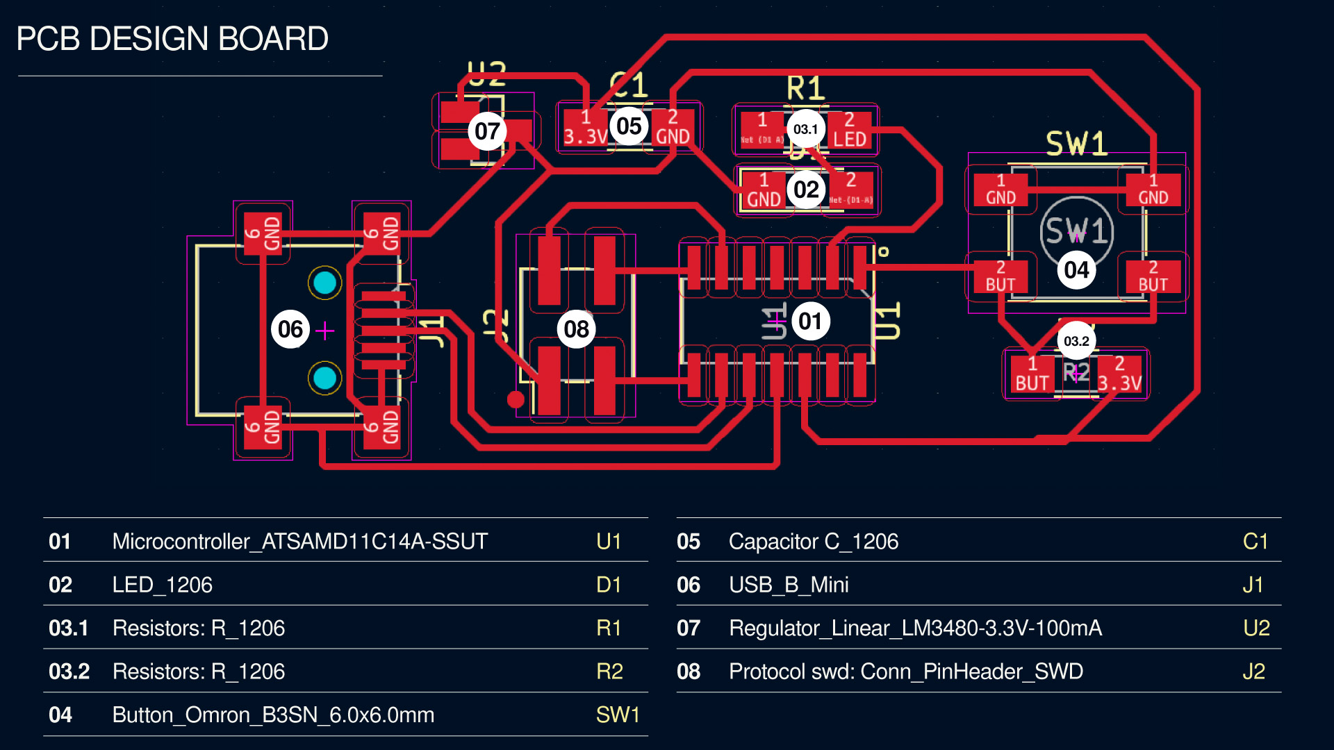
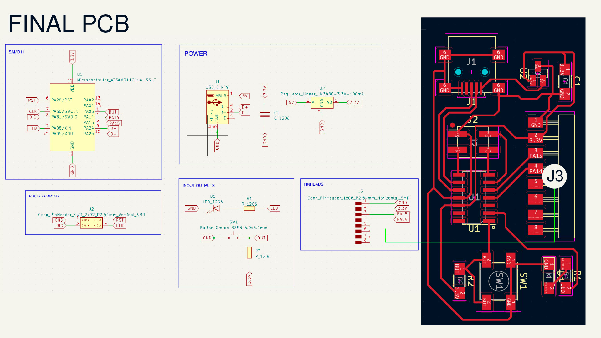
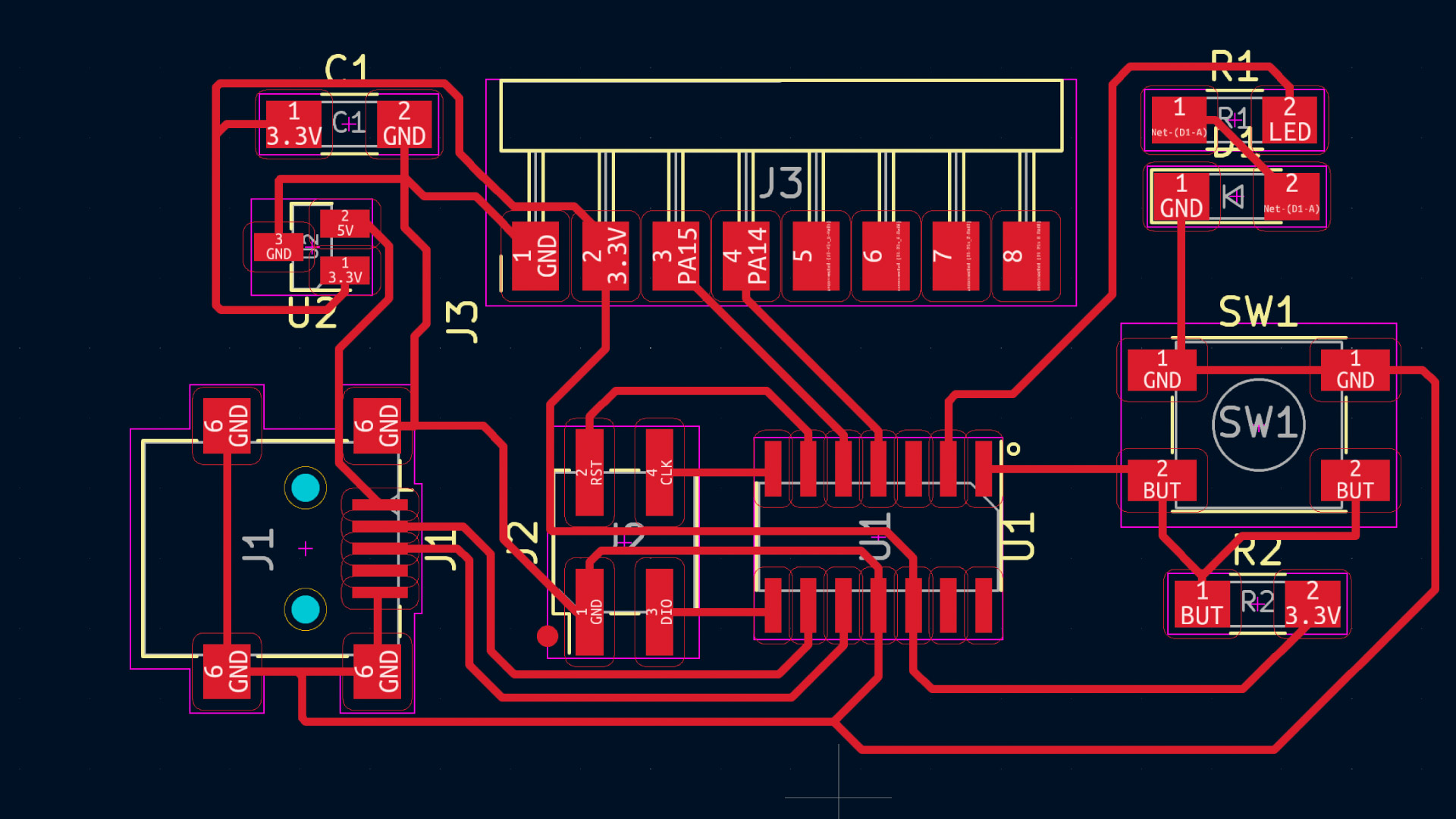
The basic components of electronics design include:

01 Power sources Power sources are the devices that provide electrical energy to a circuit. For example, a battery, but there are other sources like: generators, solar panels, and more.
02 Resistors Resistors are used to limit the flow of current in a circuit. They resist the flow of electricity because of this, they can be used to control the voltage and current in a circuit. (Always measure in OMs), There is a color code where the bands tell us the amount.
03 Capacitors They store electrical charge and release it when needed. They are commonly used in filters, oscillators, and power supplies.
04 Diodes Semiconductors that allow current to flow in one direction and block it in the other.
05 Pull up or pull down resistor The pull-up resistor allow controlled current flow from supply voltage source to the digital input pins, where the pull-down resistors could effectively control current flow from digital pins to the ground.

02Kicad tutorial


For this week we needed to design a development board to interact and communicate with an embedded microcontroller. This meant to include LED, button, microcontroller and a pinhead.


01 Getting the libraries: Symbols and Footprints

The first step is to download the libraries from gitlab, in here we have the components that we will use on fab academy.
For doing this, we create a folder. Then open the terminal and write git clone + the link.
Go to manage global libraries and activate the ones we just download by the icon of a folder. (Fab.kikad_sym) Now we can unselect all of the rest.
Then do the same for the footprint: Manage footprint inactive all of them and then again go to the folder icon and click the folder (fab.pretty).

02 Schematic Editor.

In the folder just created we have different files. We need to open the Kicked_pro file, this one contain all the files.
Design a development board that can interact and communicate.( Have the pin exposes) Adding am LED and a button, and the microcontroller of our choosing.
  • ESP32: In case to use we need also the SAMD for the comms with the computer USB, and would be the same as having the Barduino so makes more sense to create another one
  • Xiaos: Recommended to use but this one is already a microcontroller.
  • Other options ESP32S3Wroom 1, Samd11, Samd21, Attinies) but the samd we would need some programmers to install them.

    03 Adding the components on the schematic.

    Add a symbol with shortcut A.
    List of components to add:
  • Microcontroller_ATSAMD11C14A-SSUT
  • LED_1206
  • 2 Resistors: R_1206
  • Button_Omron_B3SN_6.0x6.0mm
  • Capacitor C_1206
  • USB_B_Mini
  • Regulator_Linear_LM3480-3.3V-100mA
  • Protocol swd: Conn_PinHeader_SWD_2x02_P2.54mm_Vertical_SMD We started adding the SAMDD on the right side of the page shows the data sheet link, symbol and the footprint.

    Then add the LED and this needs always the resistor. With shortcut R we rotate the component and with M to move or G in case to move it with the connections. After, we added the button and in order to control it we need a pull up or pull down resistor (used between the connection of a voltage supply and a particular pin in a digital logic circuit.)
    Add the capacitor to balance if we have some shortage of current.
    Also add a Voltage regulator (of 3.3Voltage and 100mA because the samD doesn't need that much power) because we need to add power through USB and in this case we need to go to preference>symbol library and checked the name for the in Kicad the miniusb name. ( Connector and Connector_Generic).
    We need a boatload for programming the SamD, the protocol that we will be using its called SWD

    04 Label schematics for connections

    We need to add the global labels, and after the connections we could organise it, the USB, capacitor and voltage regulator are for power, LED and button, as components that we will use. Once that is done all of the groups organice. We need to save the file.


    05 Electrical Rule Check (ERC) and Design Rule Check(DRC).

    This two features check the electrical connectivity and integrity of a circuit design, is it crucial to check both of them to for the functionality onces printed the circuit board. For example, in my SAMD11 not all of the pins where connected, so it showed the alert in the ERC in the schematic editor, while the DRC showed alerts about the clearance specially in the USB pins that are too close to each other, so instead of making it 0.4 as all of them, here I made them into 0.38.


    06 PCB

    We click the icon that says update PCB with changes made to schematic
    It will come out an error, missing is to connect the usb pin, for this first we need to go to preference>manage footprint library and add the connector USB, then on the schematics, press ā€œEā€ over the symbol of the usb in the Power group, and a pop up window of Symbol properties will apear. On the footprint if we click we get an icon of a library, and look for Connector_USB:USB_Mini-B_Lumberg_2486_01_Horizontal. Then update the same icon as before.

    The next step is to organise the configuration(the image above is how it looks when you open the pcbboard editor before organizing it). In the process we saw that made more sense to have the LED in pin02 so we moved it on the schematic and update the changes to the PCB. (The thicker the wire the more current it can flow )
    We need to go to edit board set up and then in Net classes.
    The clearance is the distance between the traces, so this one is always 0.4, 0.3 for the track width, Via is a hole that connect the bottom and top. Then click and in edit go to Edit track & Via properties and click the option set to net class values.

    07 Router

    Before the router:
    We need to connect all of the labels together, so on the right vertical toolbar there is an option call router or X as the shortcut. The line shows a red line in the middle and a grey around it, this one would be the clearance so always 0.4, we could see on the footprint that there is a really thin line around the components, these are the clearance, so in the case of the USB we need to adapt it to make it work. For this, we need to choose E over the elements, to get to the Pad properties. On the pad size X we choose 0.38, for future occasions we can save this one on the fab library by opening in the footprint editor.

    Router: The first part would be not to have straight corners, and once a line is done we could select it all with shortcut u, then e for checking that it is using net class widths. In case that we want to move any element with the connections we would have to use letter ā€œDā€

  • 03Make it work

    Pinhead


    After the class, we had to add a pinhead in order to complete the weekly assigment, for this one I used Conn_PinHeader_1x08_P2.54mm_Horizontal_SMD and connect it to: Ground, 3.3 volts and then two pins on the SAMD11 the PA14 and PA15, for future communication.
    Becuase of this change, I had to restart most of the connections in order to leave the pinhead usable. This is the final result:


    FILES


  • Kicad files

  • next project

    Computer-controlled Machining