9. Embedded Programing
Assignment Overview
Group assignment
- Compare the performance and development workflows for other architectures
- Document your work to the group work page and reflect on your individual page what you learned
Individual assignment:
- Read the datasheet for your microcontroller
- Use your programmer to program your board to do something
Learning outcomes
- Identify relevant information in a microcontroller datasheet.
- Implement programming protocols.
Group Assigment
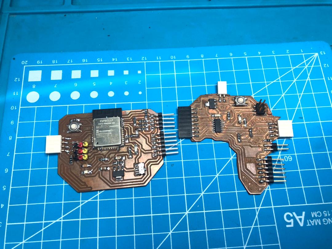
For the working group, we chose to compare the ATtiny1614 microcontroller-based Africa Board with the ESP32 microcontroller-based board I designed for the input devices assignment.
ATtiny are a subfamily of 8-bit AVR microcontrollers. The ESP32 is a series of System on Chip (SoC). They contain a Tensilica Xtensa LX6 microprocessor, WiFi, and integrated Bluetooth. It was developed to have low consumption and low cost
| Specifications | ESP 32 | Attiny1614 |
|---|---|---|
| Type | 32 bit | 8 bit |
| Data memory | 4Mb | 256b |
| ADC | 18 | 10 |
| GPIO | 34 | 12 |
| Flash Memory | 16Mb | 16Mb |
| SRAM | 520kb | 2 KB |
| f_CPU (max) | 240MHz | 20 MHz |
| Operating Voltage | 3.3V | 5V |
Flash programming and debugging protocols:
-
Attiny1614 is programmed through the UPDI protocol, which is a protocol acting as a serial port on a single bi-directional wire. A reserved UPDI pin on the ATtiny will trigger a reset whenever the voltage is set to 0V.
-
ESP32 is programmed from the Serial port, so we only use the FTDI cable to program it.
Check Input devices week for an example on how to program the ESP32.
Check Electronics design week for an example on how to program the ATiny1614.
Individual Assigment
The individual assignment consisted of two tasks. The first was to read and understand that data shee for the microcontroller you are programming, and the second is to program the board. We will begin by discussing that datasheet.
ATtiny1614 Datasheet
The ATtiny1614 is a members of the tinyAVR® 1-series of microcontrollers.
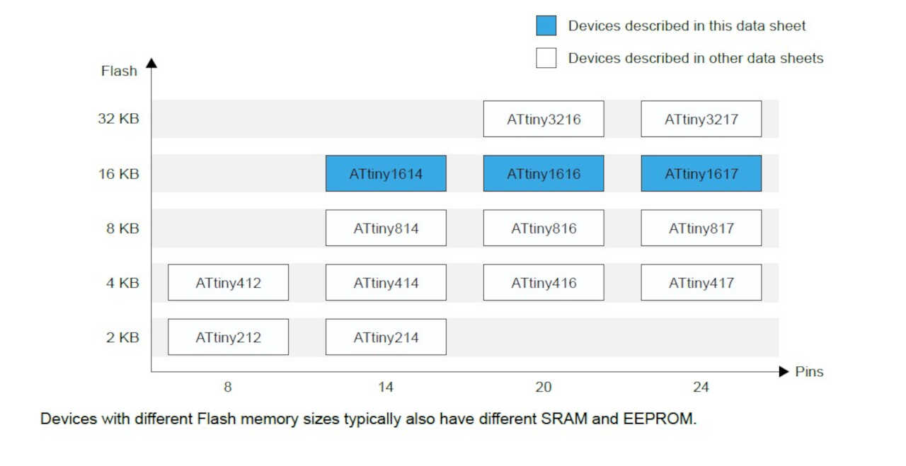
It use the AVR® 8-bit processor with hardware multiplier, running at up to 20 MHz and with 16 KB Flash, 2 KB of SRAM, and 256 bytes of EEPROM in a 14-pin package. Below are some of the specifications:
CPU: AVR 8-bit CPU running at up to 20 MHz
Memories: 16 KB in systemp self-programmable flash memory
- 256 bytes EEPROM
- 2 KB SRAM
- Write/erase flash 10,000 cycles, EEPROM 100,000 cycles
System: Power-on reset
- Brown out detection
- Internal and external clock optionn
- 16/20 MHz lower-power RC oscillater
- Single pin programming and debugging interface (UPDI)
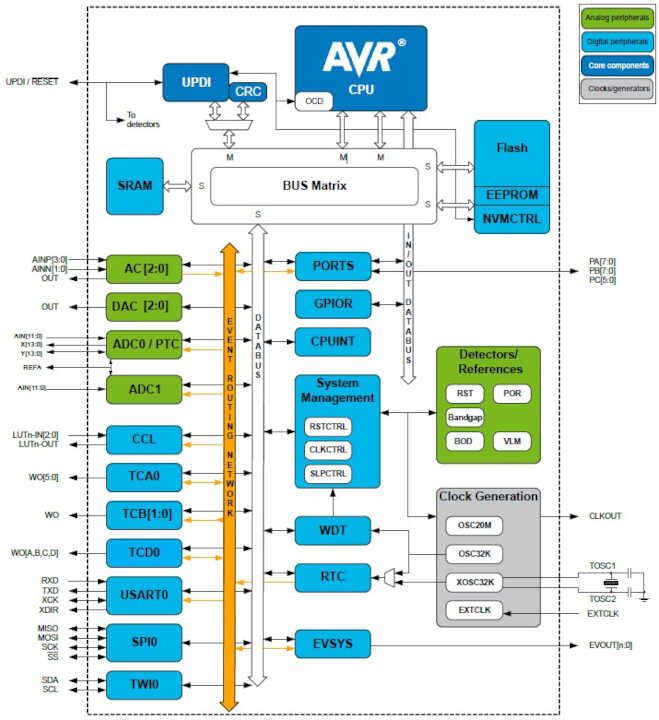
Block diagram
One of the first and most critical diagrams in the spec sheet is the block diagram. This diagram gives an overiew of the chip internals, system details, peripherals, and provides an idea of the I/O of the chip. The image below is presents the block diagram for the AT-tiny 1614. (p. 13, Figure 3-1)
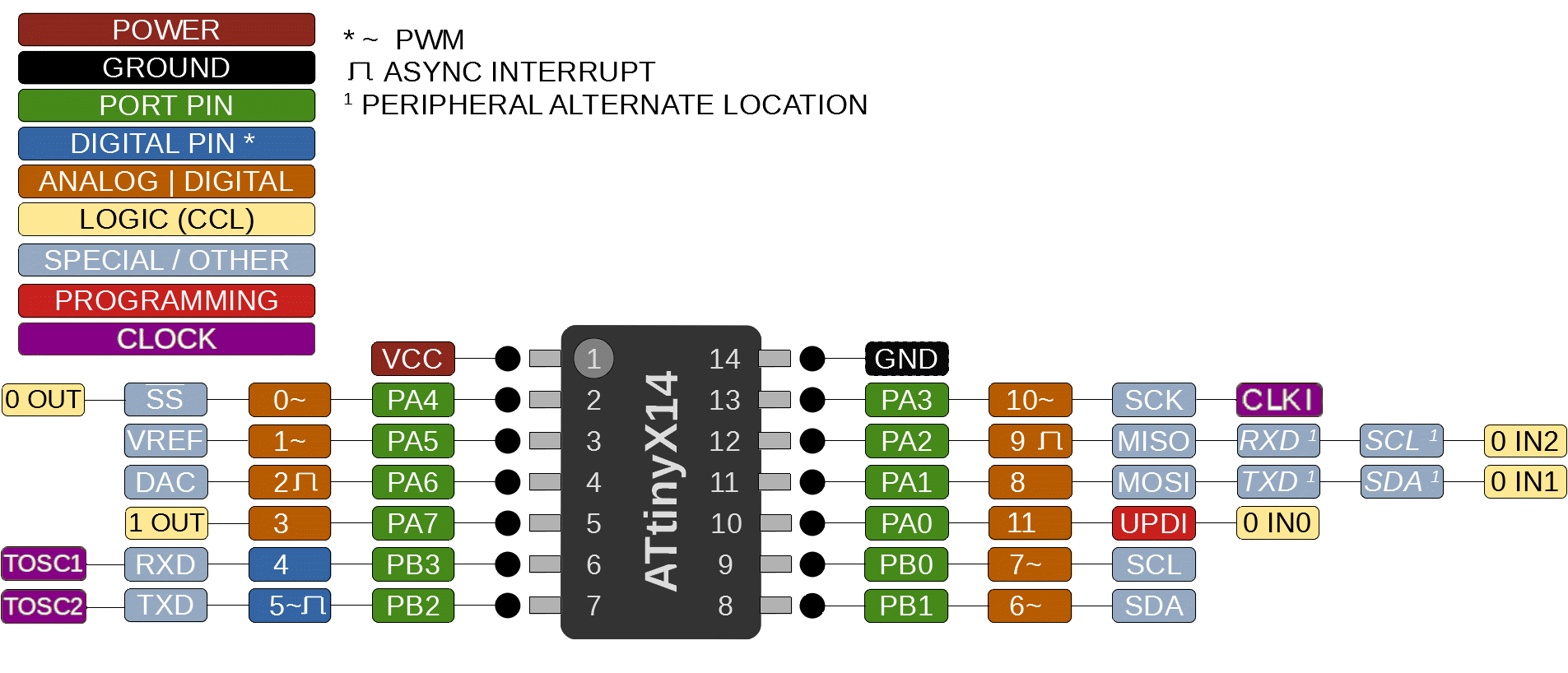
Pinout
The next diagram of importance in the spec sheet is the pinout. The pinout describes the which peripherals and I/O types are available at each pin. The image below presents the pinout. (p.14, Figure 4.1)
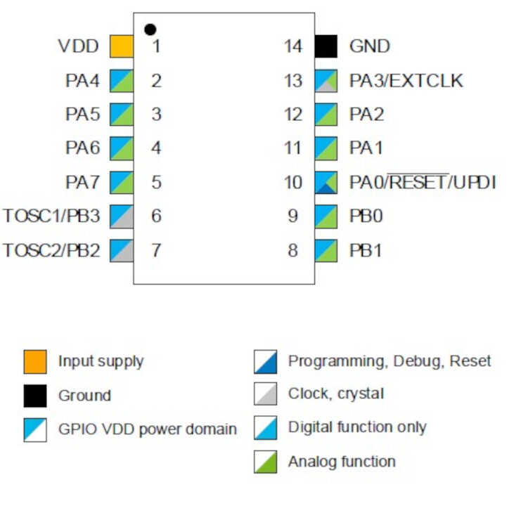
The important pins to consider for the AT-tiny are the VDD (pin 1), the GND (pin 14), and the UPDI (pin 10). Other important pins to pay attention to are:
- Pins 2-5, 8,9 11, 12: Digital/analog functions to read or output to peripherals
- Pins 6 and 7: GPIO and clock
- Pin 13 GPIO/Clock/Analalog function

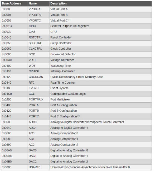
Peripheral Module Address Map
The ATtiny 1614 has numerous peripherals with various addresses below is a list of the types of peripherals it contains:
- Virtual Ports (A/B)
- I/O registers
- CPU
- Reset controller
- Sleep controller
- Clock Controller
- Brown-out detector
- Voltage reference
- Port configuration
- Analog comparators
- Digital-to-Analog converters
- Universal Synchronous Asynchronous Receiver Transmitter
- Serial Peripheral interface
- Timer/counter
- System configuration
This information can all be found in the peripherals section (p. 42, Section 7) and is all neatly summarized in Table 7-1 as illustrated below.
Details of each peripheral are given in the chapters that follow. We will not discuss them in detail here. The last two things we will discuss before moving ahead to programming the board will be the CPU and the UPDI.
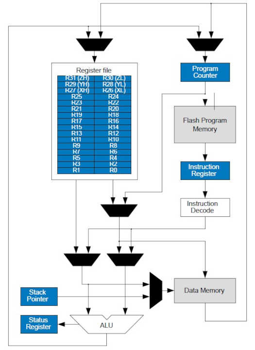
AVR CPU
The AVR CPU uses 8-bit AVR CPU. The CPU is able to access memories, perform calculations, control peripherals, and execute instructions in the progrm memory. This CPU uses a HARVARD Architecture with seperate buses for program and data. Instruction in the program memory are executed with single-level pipelining. While one instruction is being ecuted, the net instruction is prefetched from the program memory, which enables instruction to be executed on every clock cycle. (p.48, Sections 8.1-8.3). The features of this AVR CPU are:
- 8-Bit, High-Performance AVR RISC CPU
- 135 instructions
- Hardware multiplier
- 32 8-Bit Registers Directly Connected to the Arithmetic Logic Unit (ALU)
- Stack in RAM
- Stack Pointer Accessible in I/O Memory Space
- Direct Addressing of up to 64 KB of Unified Memory:
- Entire Flash accessible with all LD/ST instructions
- True 16/24-Bit Access to 16/24-Bit I/O Registers
- Efficient Support for 8-, 16-, and 32-Bit Arithmetic
- Configuration Change Protection for System Critical Features
A block diamgram that illustrates the architecture is shown below:
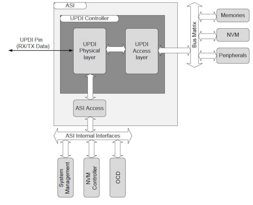
UPDI
The UPDI is an interface for external programming and on-chip debugging of a device. The UPDI supports programming of nonvolatile memory (NVN) spalce; FLASH, EEPROM, ukbi and the user row. Furthermore, the UPDI can access the entire I/O and data space of the device. Programming and debugging are done the the UPDI Physical interface (UPDI PHY), which is a 1-wire interface that uses the RESET pin. The UPDI access layer grants access to the bus matrix, with memory mapped access to system blocks such as NVM, and peripherals. (p.516, Section 33.2). The fueature of the Unified Program and Debug Interface are as follows (p.516, Section 33.1):
Programming:
- External programming through UPDI 1-wire (1W) interface
- Enable programming by 12V or fuse
- Uses the RESET pin of the device for programming
- No GPIO pins occupied during operation
- Asynchronous Half-Duplex UART protocol towards the programmer
Debugging:
- Memory mapped access to device address space (NVM, RAM, I/O)
- No limitation on device clock frequency
- Unlimited number of user program breakpoints
- Two hardware breakpoints
- Run-time readout of CPU Program Counter (PC), Stack Pointer (SP), and Status register (SREG) for code profiling
- Program flow control -> Go, Stop, Reset, Step Into
- Non-intrusive run-time chip monitoring without accessing system registers -> Monitor CRC status and sleep status
Unified Programming and Debug Interface (UPDI):
Built-in error detection with error signature readout requency measurement of internal oscillators using the Event System
Programming
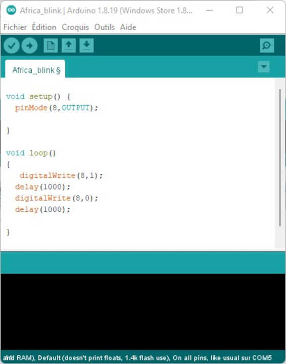
In the Arduino software,by navigating to File > Examples > 01 Basics > blink you can open the blink sketch. To see what Arduino pin numbers are associated to it, you need to find the Arduino pinout overview. I googled “ATtiny1614 Arduino pinout” to see if I could also make the blinking work while using the pin number that the LED is connected to according to Arduino/megaTinyCore.
I found several Fab Academy websites that showed images of the pinout. One site pointed to the source of the pinout in the megaTinyCore documents:
For this board change the pin number to Pin 8, which is the pin that the LED is wired to. You can do this by replacing LED_BUILTIN in the code with 8. Once finished click upload.
Pressing the button
My button is connected on the PA3 pin of the Atiny which corresponds to the number 10 for the arduino library. I’m going to program the button to have the function of on/off switch for the led
    const int led = 8;
    const int buttonPin = 10;
    boolean oldbuttonState = LOW;
    boolean newbuttonState = LOW;
    boolean LEDstatus = LOW;

    void setup() {
    pinMode(led, OUTPUT);
    pinMode(buttonPin, INPUT);
    digitalWrite(led, LOW);
    }
    void loop() {

    newbuttonState = digitalRead(buttonPin);

    if (newbuttonState != oldbuttonState)
    {
    if (newbuttonState == HIGH )
    {
        if ( LEDstatus == LOW )
        {
            digitalWrite(led, HIGH);
            LEDstatus = HIGH;
        }

        else
        {
        digitalWrite(led, LOW);
            LEDstatus = LOW;
        }
    }
    oldbuttonState = newbuttonState;
    }
    }
What went wrong/What went well
It was a very good week for me, I had no problems and everything worked as planned.