7. Electronics Design
Assignment Overview
For this weeks assignment, we were tasked with designing, milling, soldering, and testing our own circuit board. The purpose of the assignment is to familiarize ourselves with the desgin tools and software (such as KiCad) and also how to test and debug a board. The details of the assignment are below.
-
Group assignment
- Use the test equipment in your lab to observe the operation of a microcontroller circuit board (in minimum, check operating voltage on the board with multimeter or voltmeter and use oscilloscope to check noise of operating voltage and interpret a data signal)
- Document your work to the group work page and reflect on your individual page what you learned
-
Individual assignment
- Redraw one of the echo hello-world boards or something equivalent, add (at least) a button and LED (with current-limiting resistor) or equivalent input and output, check the design rules, make it, test it. Optionally, simulate its operation.
-
Learning outcomes
Select and use software for circuit board design Demonstrate workflows used in circuit board design
Group assignment
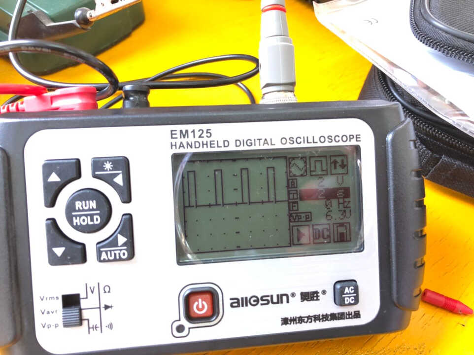
The group work involved using test equipment in the lab to observe the operation of a microcontroller circuit board using an oscilloscope and voltmeter. This week we used the equipment to check the final circuit board created for the individual work.
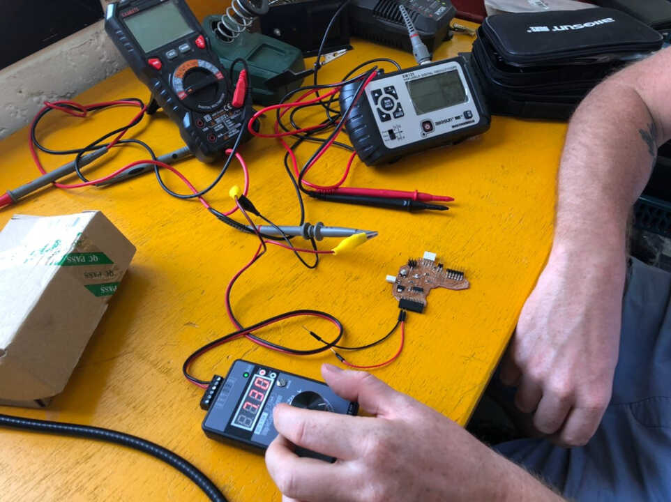
We used the small voltage generator to power the different current sources on the board (9v and 5v).With the multimeter we could test the components such as the capacitor, the led, the linear regulator, the button and the continuity between the pins. After these different tests, we uploaded a flashing program of the led on the board and thanks to the oscilloscope we have to observe the digital signal at the output
Individual Assigment
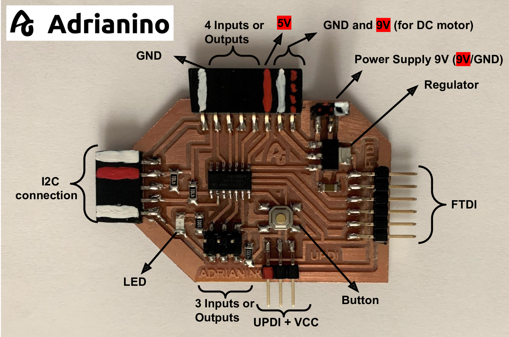
The objective of this assignment was to redesign an existing circuit board using a design software of your choice and add a button and LED to it. The assignment called for the creation of the hello-world echo board, so we will be making the Adrianino, a board developed by Adrian Torres of the Fab Academy that uses the Arduino IDE programming language. A picture of the Adrianino in the image below. You can also find all the details about the design on Adrian Torres’ Fab Academy site.
The following sections will detail, step-by-step the design process used to draw the board like Adrianino using kiCad.
KiCad
In this section I will discuss the steps that were taken to learn electronics design. Beginnig with installation and learning of the program (KiCad), through to drawing a board and finalizing the trace to be milled.
The main program to design our board with is KiCad and open-source electronics design automation suite. It’s a collection of several different programs that work together to help in the design of a PCB.
Libraries
To make it a lot easier to design my board, I had to add several symbol and footprint libraries to it. Specifically the Fab Electronics Library for KiCad that contains the symbols and footprints of (almost) all the parts that we’ll be using during the Academy.
For the installation process I recommend this video that was really useful to me, created by Fab Academy’s Kris of Aalto Fab.
Learn Kicad Schematic Editor
Now that all the libraries are installed, we can start creating our electronic schematics. To start editing schematics in Kicad, just click on the icon shown in the image below.
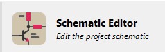
We can see below how the Kicad interface looks like for the creation of an electronic schematic.
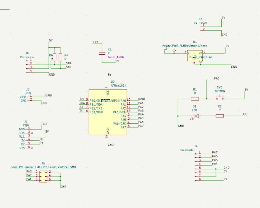
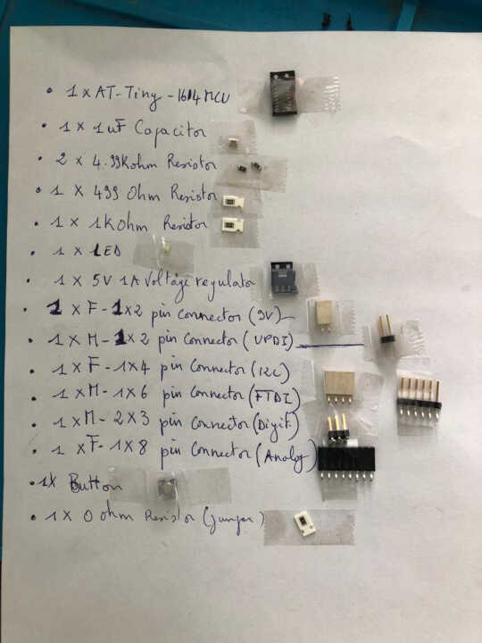
Since I am inspired by the Adrianino board, here is the list of components I need to create my board
- 1 x AT-Tiny-1614 MCU
- 1 x 1uF Capacitor
- 2 x 4.99 kOhm Resistor
- 1 x 499 Ohm Resistor
- 1 x 1 kOhm Resisitor
- 1 x LED
- 1 x Button
- 1 x 5V 1A Voltage regulator
- 1 x F-1x2 pin connector (2.54mm)
- 1 x F-1x8 pin connector (2.54mm) for I2C
- 1 x F-1x4 pin connector (2.54mm)
- 1 x M-1x6 pin connector (2.54mm) for FTDI
- 1 x M-1x2 pin connector (2.54mm) for UPDI
- 1 x M-2x3 pin connector
To insert the components in the workspace for the schematic edition we just have to click on the icon below

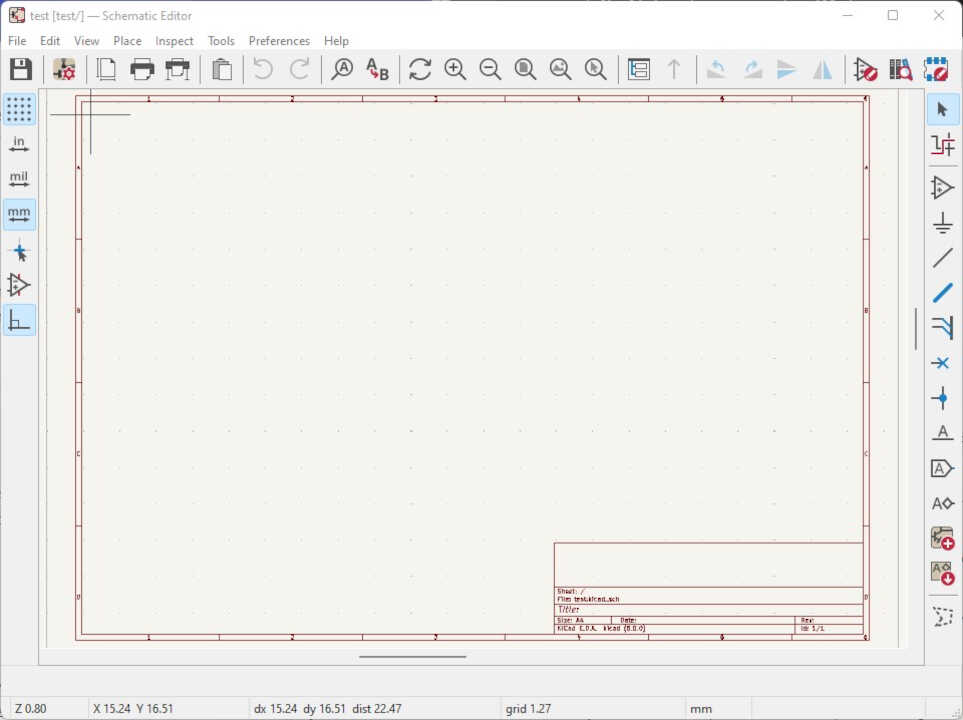
We can also use the A button on the keyboard as a shortcut to achieve the same result. We have a window that opens in which we will have to write the name of the component that we want. The image below shows that I am choosing a resistor.
Press OK and click the board at the location where you want to place the symbol. In case you aren’t happy with the location, hover your mouse over the component and press M to move or R to rotate the part.
To place another component press A, which will open the Choose Symbol menu again. However, in case you simply want to add the same component, hover over the one already on the schema and press C to copy it to your mouse and click anywhere to place it.
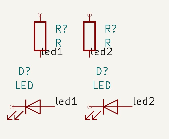
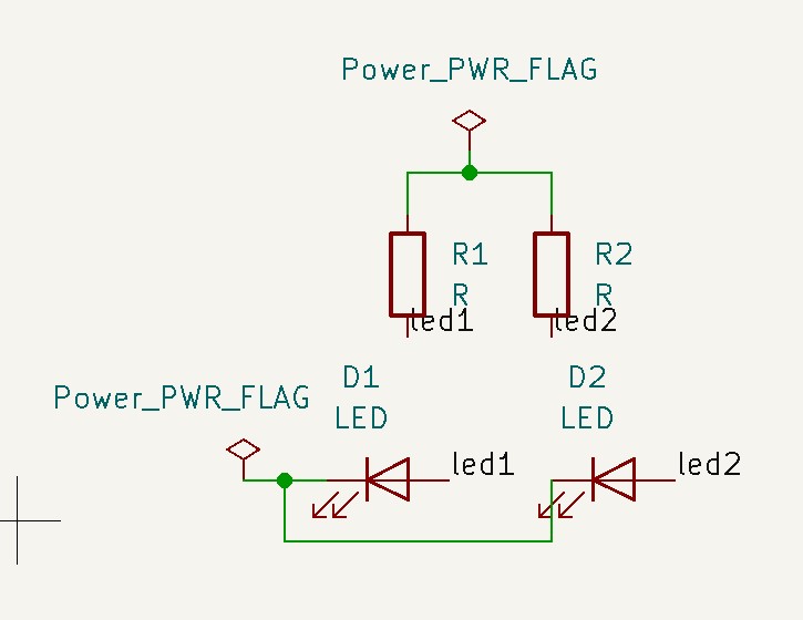
You can see in the picture below that I inserted only two resistors with two leds, just to show how you can connect the components together.
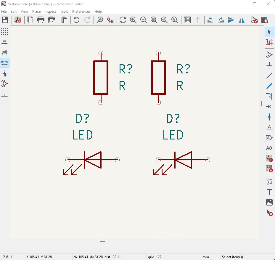
To link the components together we can click on the W key of the keyboard or click on the icon shown below
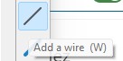
We can now connect the components as shown in the picture below.
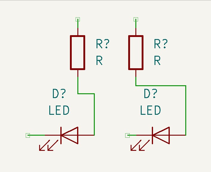
We have another way to connect the components by using labels that will be used to name the connection points of the components. To use the label we can click on the L key for the keyboard shortcut or click on the icon shown in the image below.
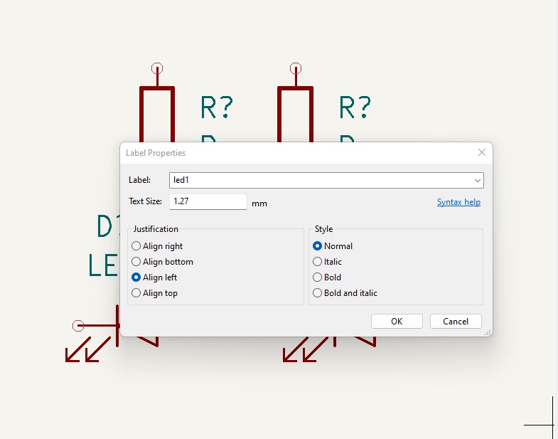
To join two points you just have to name these points with the same name. The image below shows the interconnection of the components with the labels
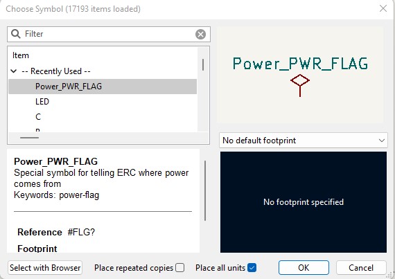
To finish our schematic and to make a verification test, it is important to add some elements:
- The Powerflag which allows the software to know the input and output points of the electrical energy in the schematic.
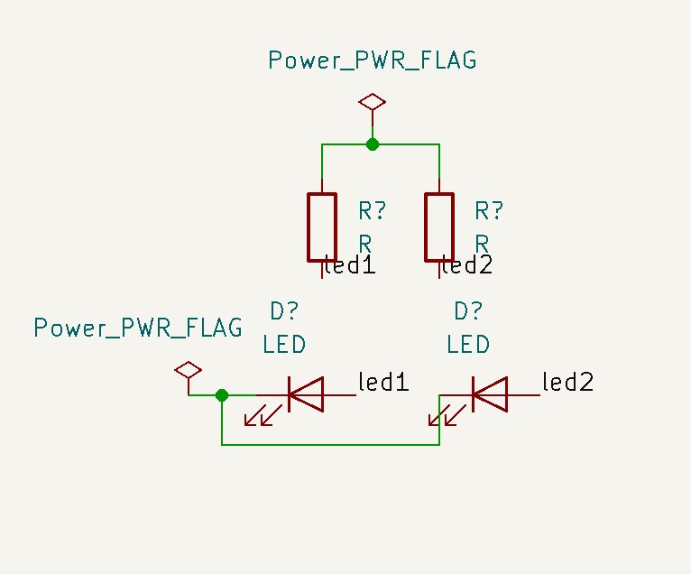
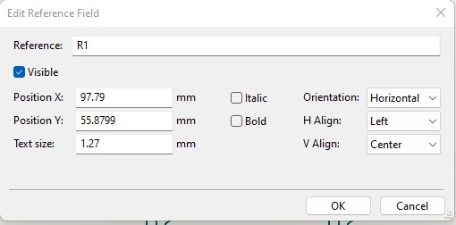
- Referencing of each type of component used
We can now verify that our schematic respects all the rules by clicking on the Inspect>Electrical Rules Checker tab.
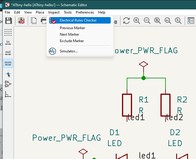
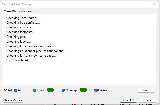
In the window that opens, we click on the Run ERC button to start the verification. We have bullets at the bottom of the window that tell us the number of errors and the number of warnings.
The micro-controller used at the heart of the board is called the AT-Tiny 1614 microcontroller. Its design specs can be found here. A photo of the pinout is included below:
-
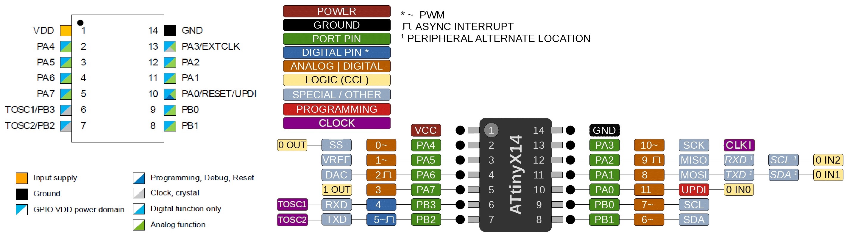
- VDD: Supply voltage.
- GND: Ground.
- Digital pins: Port A: PA0, PA1, PA2, PA3, PA4, PA5, PA6, PA7. Port B: PB0, PB1, PB2, PB3.
- Analog pins: PA1, PA2, PA3, PA4, PA5, PA6, PA7. Port B: PB0, PB1.
- UPDI Programming pin: PA0 (physical pin number 10). External Clock Pin: PA3.
In the image below you can see that I have inserted all my components, interconnected with lines and also with labals as I had shown above.
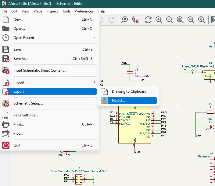
To finish with the schematics editor, we need to export our work into a .net file which will then be imported into the PCB Editor.
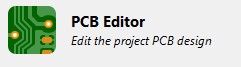
PCB Editor
To open the PCB editor we can click on the icon shown below
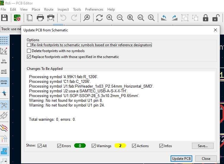
Now in the PCB editor, you can either import the Netlist you exported in the schematics window .
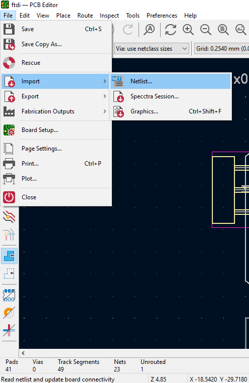
I prefer using the shortcut Key [F8]. When you press [F8] it will autmatically pick up the symbols in the schematic window and update your PCB editor work space with it.
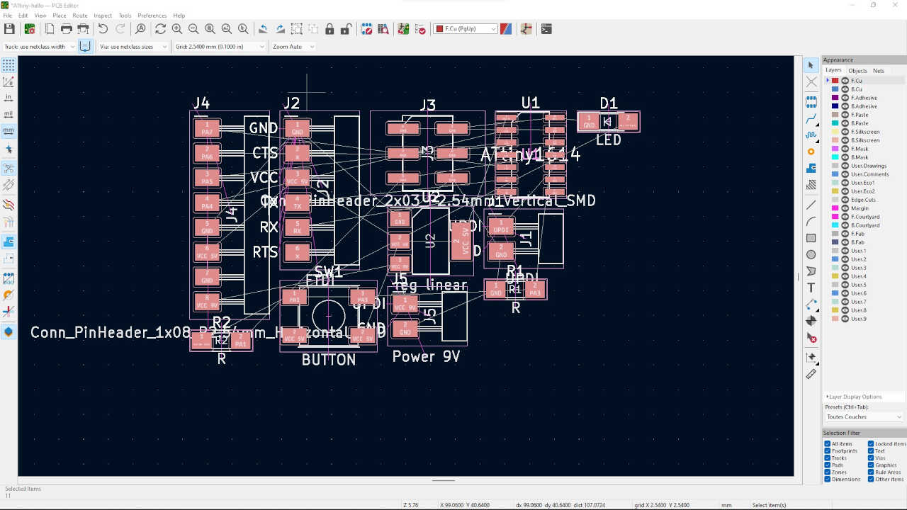
you can move the footprints to places and alignment of your choice.
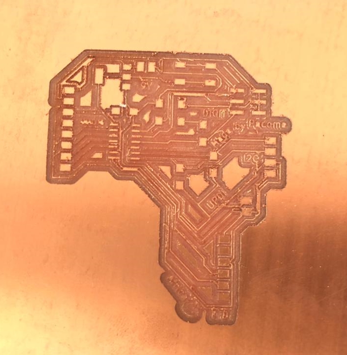
Now this was my strategy I used to lay my traces without any problem This below shows the circuit in the KiCAD PCB editor window with the footnotes of the symbols used in the Schematic editor and the copper traces that does the connections.
Track width = 0.7mm
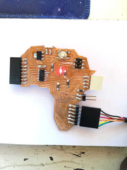
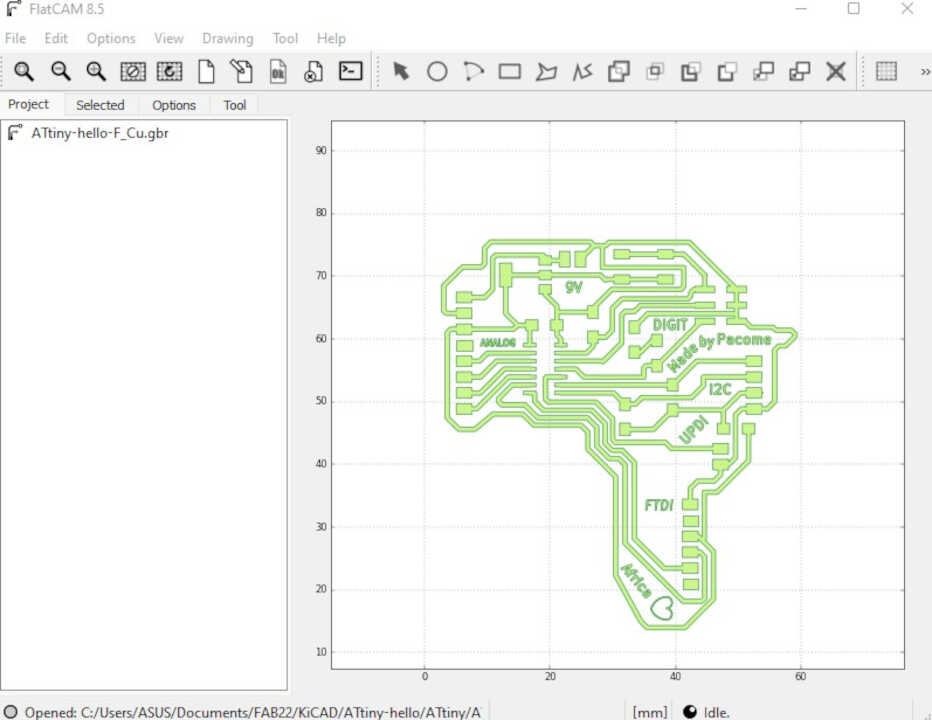
For a thought to my dear continent, I design my board in the shape of Africa.
Now this was my strategy I used to lay my traces without any problem This below shows the circuit in the KiCAD PCB editor window with the footnotes of the symbols used in the Schematic editor and the copper traces that does the connections.
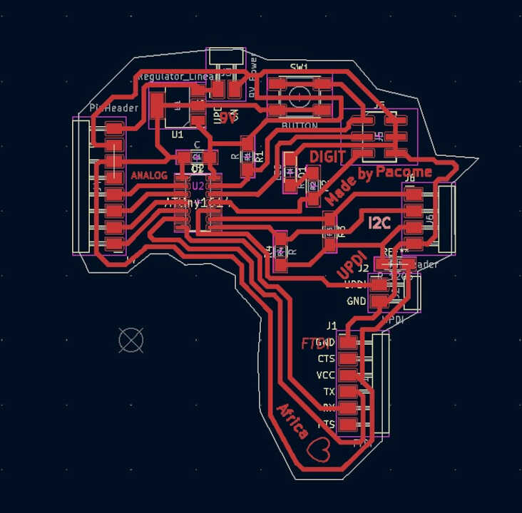
After finishing, I export my board layout to a gerber file by clicking on File>Fabrication Outputs>Gerber(.gbr)
Milling and soldering
Flatcam
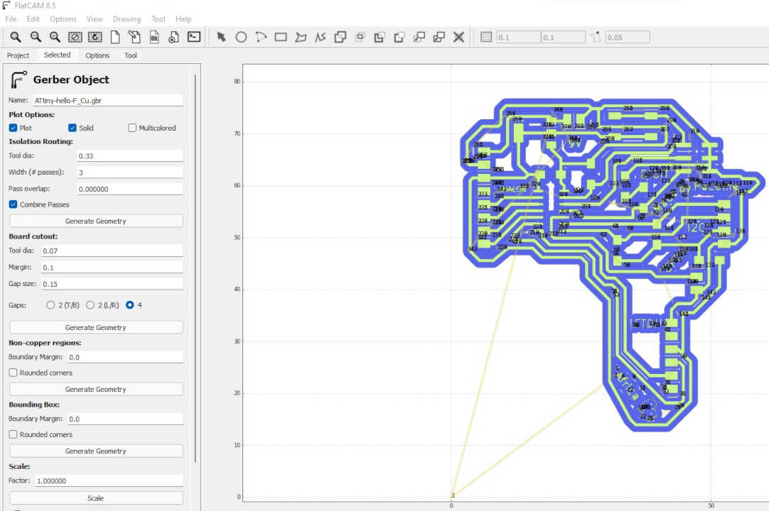
We use flatcam to generate the gcode for the cnc. First we open the gerbe file in flatcam
For milling the traces of the board we used: - tool diameter: 0.33mm tool depth: 0.08mm - feed rate: 60mm/m - spindle speed: 11000rpm - travel z: 2mm - cut z: 0.08mm
For milling out the board cut these were the best parameters used: - tool diameter: 1mm - travel z: 2mm - cut z: -1.5mm - feedrate: 90mm/m - spindle rate: 11000rpm
Mill the circuit board
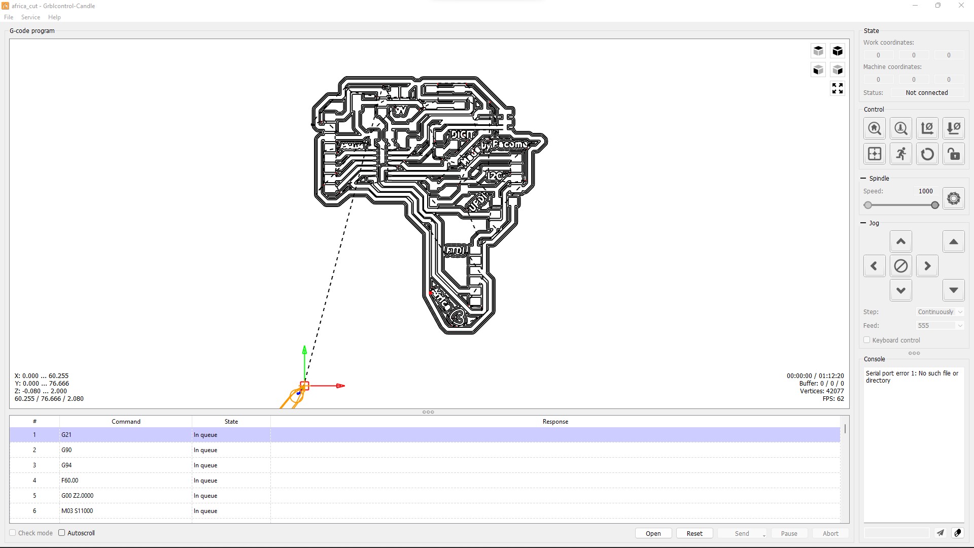
The next step in the workflow is to mill your circuit board. For this step we used a mini cnc 1610 pro machine, with details describing operation and characerisation given in Assignment 5 - electronics production
We use grb control sofware to control the cnc
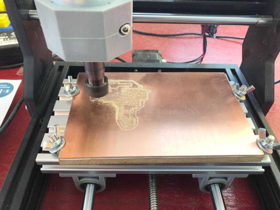
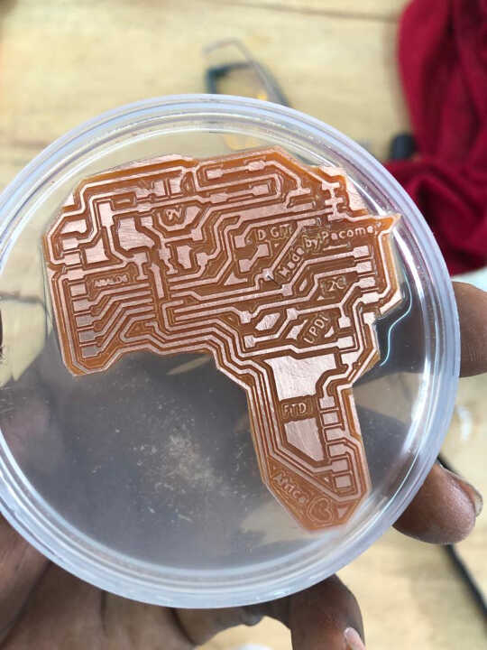
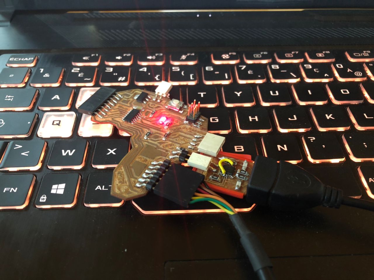
Once the milling was completed. The next step in the process was to solder the board. Below is a photo of the final milled board
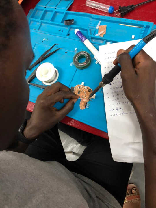
Solder the components onto the circuit board
To solder the components on to the board. A photo of the components is shown below:
Below is an image of the final board after it was soldered:
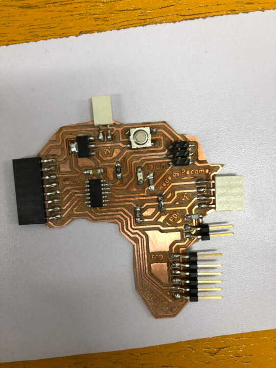
Once the board was soldered, the next step in the process is to program the board. Those details will be discussed in the next step.
Program the circuit board
The circuit board that was constructed was designed to be compatible with Arduino IDE and thus reprogrammable based on the functions that you want it to perform. In this section we will discuss how to program the standard “blink” sketch onto our AT-Tiny board. The steps are as follows(for windows OS):
-
Install Arduino IDE
-
Download and install the AT-Tiny board library
-
Set the board configuration and port
-
Upload the blink sketch using Arduino
Before starting the steps mentioned above, we need to connect our board to our computer. To do this we connect the updi card produced in week 5 about electronic production. In addition to the UPDI board we use the FTDI connection cable to just power the board. The picture below shows how to connect the hardware:
Install Arduino IDE
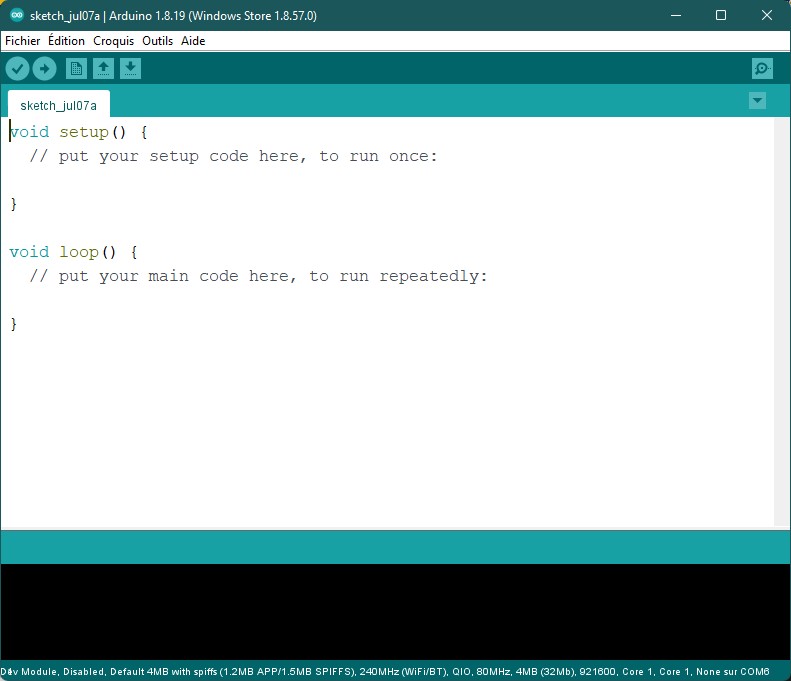
You can download the Arduino software at this link
After installing it, here is how its interface looks like
Download and install the AT-Tiny board library
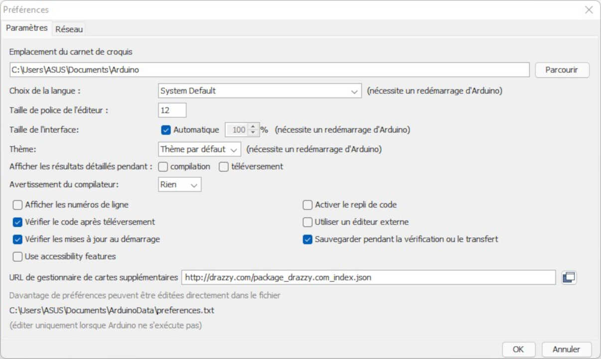
Now we have to install the AT-Tiny board library. To install it we open the Preference window by clicking the File>Preferences tab
Inside the window, in the space reserved for the additional board manager url, we paste this link :
http://drazzy.com/package_drazzy.com_index.json
After clicking on the ok button, we go to the Board Manager as shown in the image below.
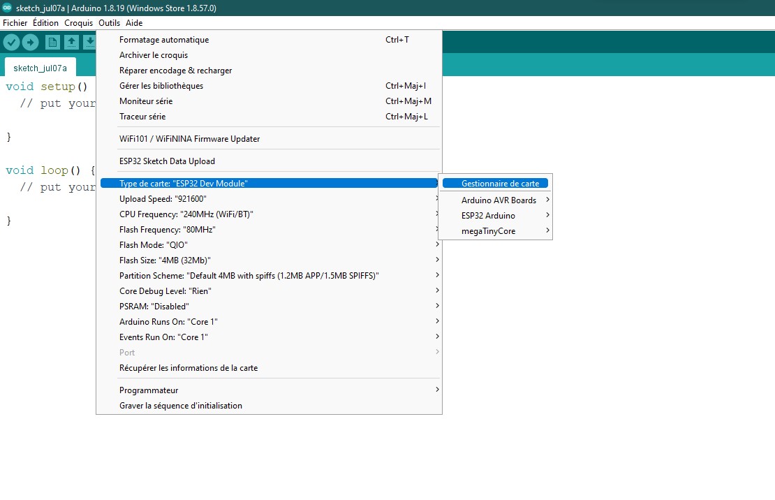
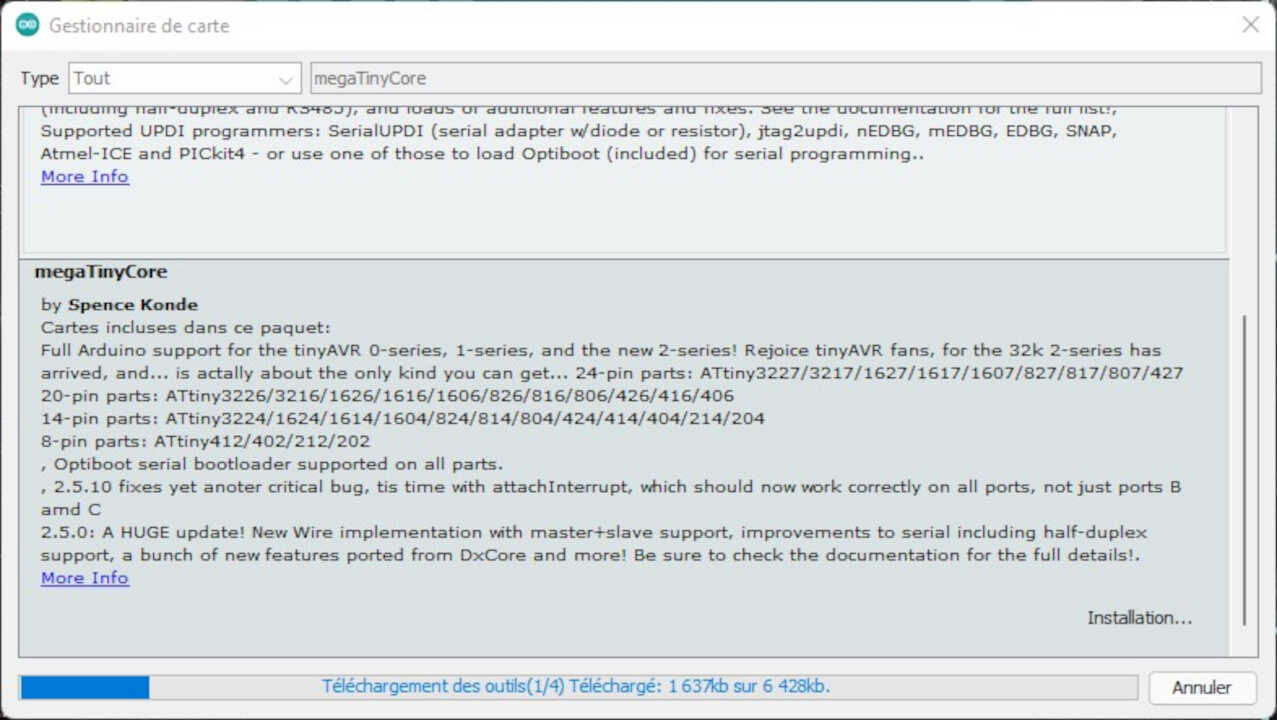
In the board manager window we look for the megaTinyCore library and install it.
Set the board configuration and port
step you will return to the Arduino IDE and load your sketch as you normally would. You will next want to set the board configuration as follows Tools > Boards > MegaTinyCore > ATtiny 1614 and you will want to set the programmer to Serial Port, Tools > programmer > Serial UPDI . Other settings to consider are the clock. To set it at 20 MHz.
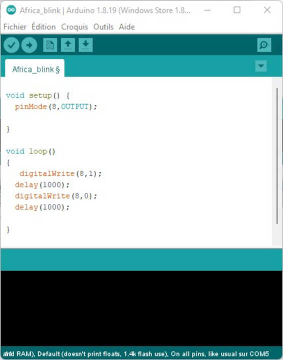
Upload the blink sketch
By navigating to File > Examples > 01 Basics > blink you can open the blink sketch. For this board change the pin number to Pin 8, which is the pin that the LED is wired to. You can do this by replacing LED_BUILTIN in the code with 8. Once finished click upload.
File
The files that were created for this assignment can be found at the following links:
review of this week
Refection
My reflection this week is mainly about the UPDI board which allows the programming of the microcontroller. The remark made is that the UPDI board alone cannot allow us to program because the microcontroller must be powered well before. The choices on my board are either to supply it with 12V or to use the FTDI cable presented above. At the output of the UPDI board we have two pins (UPDI and GND). By adding a third pin for the VCC (5V) this could have saved us other connections.
What went wrong?
- The first thing that went wrong was when I was milling my card. I had made a mistake in the flatcam software settings by reversing the tool diameter values with the Z cut. After that, here is the result below.
- The second thing that didn’t work was the fact that I broke the bit during the milling process. The mistake I made was that when I changed the bit to mill the outline of my card, I didn’t remember the Z-axis zooming. Therefore, when I started the process, the machine went to the Z-axis home of the old bit and the bit was broken.
What went well ?
For the rest of the work, everything went well and I learned from my mistakes.
What I would do differently next time ?
Next time, I’ll take the precaution of reparameterizing the z-axis setting when I change the bit to cut the edge.
Wrapping up
This week’s assignment was very exciting and rewarding for me. Although I used to develop electronic mini-projects, I have always been limited to using arduino boards and punch boards for prototyping. So this was my first time designing a personal electronic board and learning to use software like kicad and flatcam.