7. Electronics design
This week I worked on learning how to modify a designed board.
Assignments for the Week:
Group Assignment:
Use the test equipment in your lab to observe the operation of a microcontroller circuit board. You can view our results of this week’s group work here.
For this week’s group work, Barbara Morrow and I worked with the multimeter on the ATtiny412 boards we made previously in the lab.
Individual Assignment:
Redraw an echo hello-world board. Add (at least) a button and LED (with a current-limiting resistor).
Check the design rules, make it and test that it can communicate
Board re-design in KiCad
Schematic Design
For our individual assignment this week, we were supposed to redraw a board used in our lab. For our electronics production assignment in Week 5, we milled, stuffed and communicated with an ATtiny412 board created by Adam Harris. The board was then further altered by our instructor, Tom Dubick, into a “minimally viable” board, existing of the least amount of components to work. This week, we completed the assignment by taking the images of these boards, adding a button and programming them to respond.
I began the process in KiCad, the software our lab uses to design PCB boards in-house. Earlier this year, we were all given access to tutorials to work through on how to use KiCad. To complete this assignment, I had to go back and review several of those videos to refresh my memory of how to use the software.
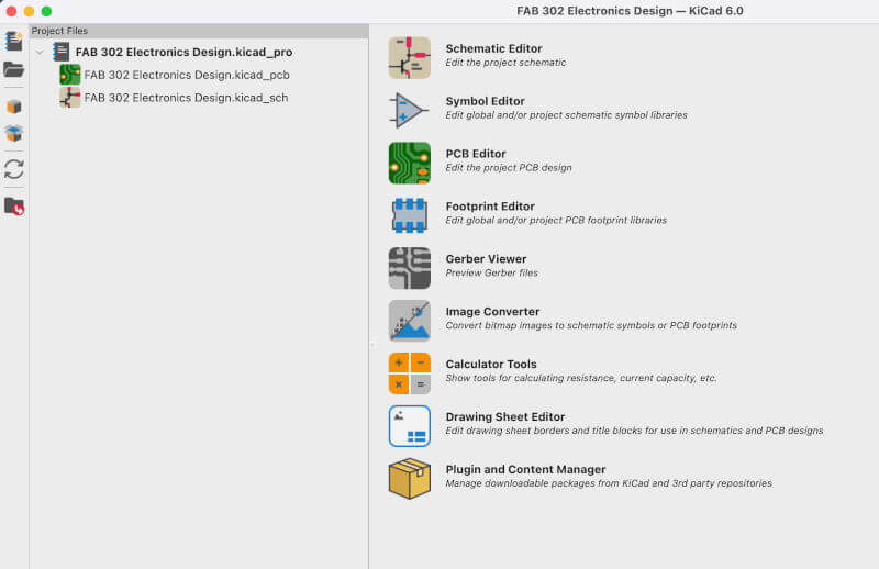
I began by setting up a project in KiCad program. When you do this, the software creates a project file (.pro), and schematic file for the project (.sch) and a PCB file for the project (.pcb). These files are all housed under the main project tab and can be accessed through each section.
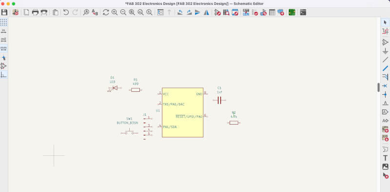
Once I set up a new project, I opened the schematic interface and began working on redrawing the board. The first step was to lay out the components by selecting them from the symbol library. After selecting the the component, you can edit it’s name, value and rotate it’s direction. Double-clicking on any specific component will also show it’s datasheet and footprint (how it looks).
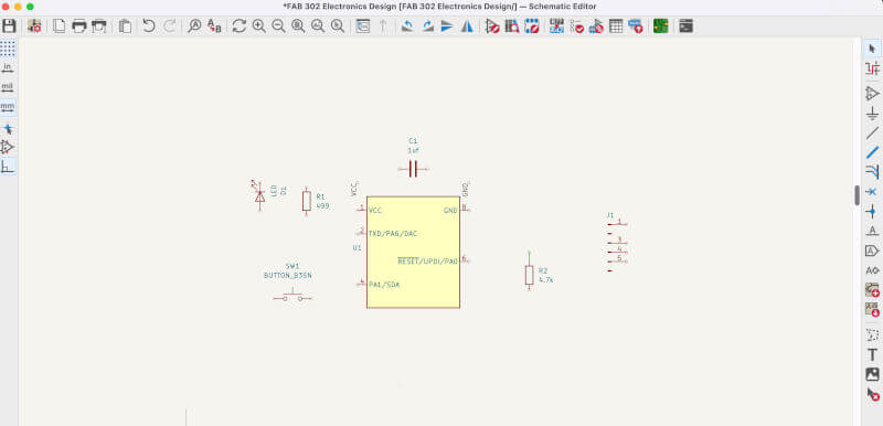
After selecting my components, I wanted to lay them out in a way that was easier for me to understand. One of the hardest parts of this process for me was that the schematic does not look like the final PCB layout. I had to restart my process several times because I kept getting thrown by this concept. I finally decided it would help me to move the components around on the board to be closer to where I actually wanted to see them on the final board. I moved and rotated them to reflect the original board design. Then, when I was ready to add the button, I made adjustments and moved things around a little more to allow it to fit.
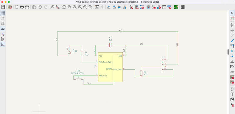
The next step is to connect the components to one another correctly. The majority of this was easy, since we were basing the design off a pre-designed board. Once those components were connected, I then added the button to the ground and pin 4 of the chip on the board. Once we get to the programming step, I will have the board “read” the status of the button and based on whether it is pressed or not, it will cause the LED to light up or stay in its current state (non-lit).
After my components were all connected, it was time to run the “electrical rules checker” (ERC). This step analyzes your schematic design and gives you warnings and errors that don’t follow the correct design rules for electronics. Some of them are just warnings that will not affect the actual design of the board.
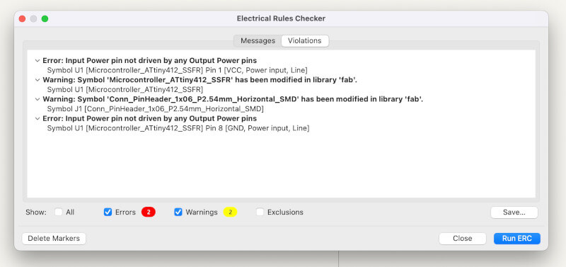
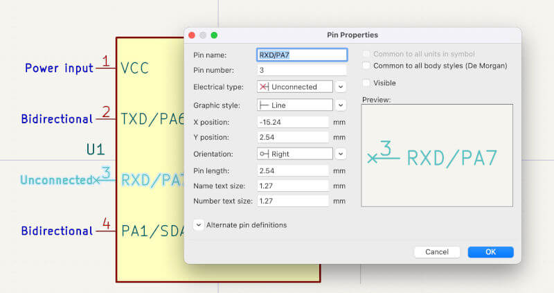
I had a few of these because I used the symbol editor to manipulate the pins on my chip and header. Because I was not using all the pins, it was advised to edit them to show they are “unconnected” and make them not “visible”. Not only will this step help clean up the overall look of the schematic, but I liked it because I wouldn’t accidentally connect a component to the wrong pin.
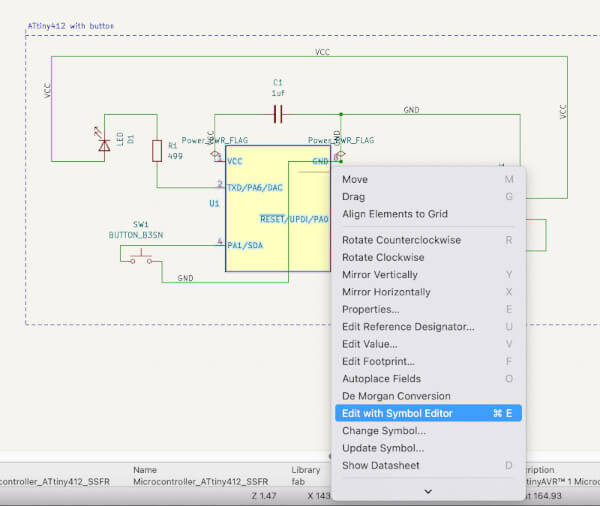
The final check on the ERC showed that my VCC and GND pins on the chip were not driven by any power pins, meaning they had no noted power supply. In order to fix this to clear the ERC, I selected the “add a power port” symbol from the right menu and added power flags to my two pins. I ran the ERC again and was happy to see I had cleared out all of my errors. The next step was to send the schematic over the the PCB Editor to design the layout of my new board.
PCB Editor and Design
Because I already had the schematic window open, I clicked on the PCB button from the top menu. It opened the PCB editor and then I clicked on fn8 to update the PCB from the schematic. (Optionally I could have also selected “update PCB with changes made to schematic” button from the top menu.) After that I clicked “update PCB”.
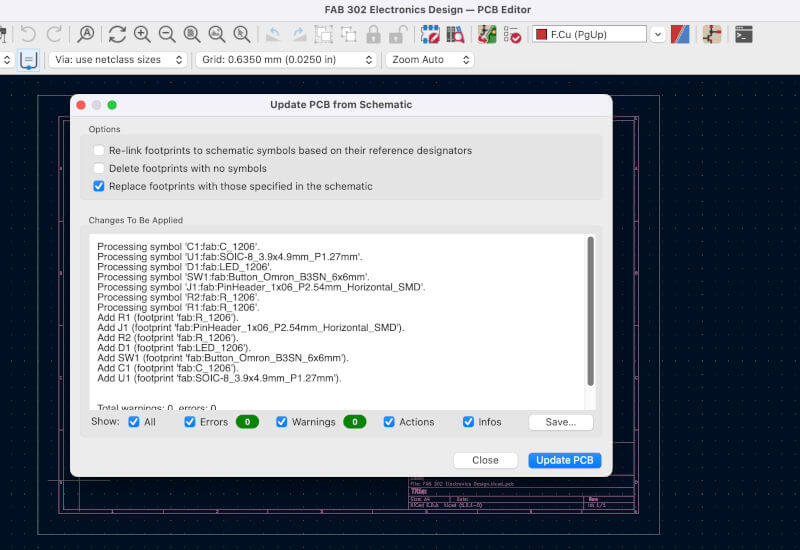
I was frustrated to see that all that time I spent laying out the components where I needed them for my final design did not carry over to the PCB editor. Of course, I knew this would be the case (since as mentioned earlier, the schematic is not designed to address the actual layout of the components). Still, in my mind, it made it easier and wasn’t a huge hassle to complete that part. I still believe it made it easier for me to understand the process.
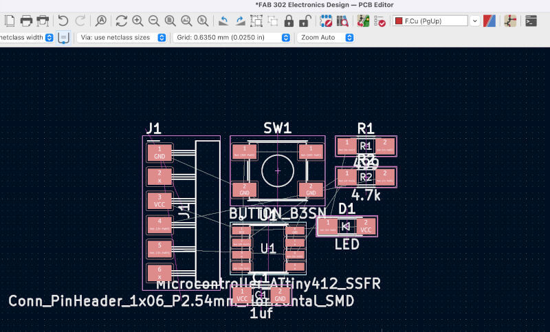
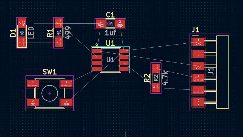
Taking that extra step earlier of laying out the design in the schematic allowed me to quickly move components around in the PCB editor. I knew exactly where I wanted them to be and in which orientation. And, although it’s a little difficult to see the thin lines, the traces created in the schematic were brought over to the editor, so the next step of adding traces went very smoothly!
Board Milling and Stuffing
Once my design was complete, it was time to mill my board. I used the same process from week 5, when we did our electronics production. This time around, the process of milling my board was great!
After milling, I gathered the components needed to stuff it. To make sure the components are all in the correct location, I used my PCB layout shown above.
LED Communication
Stuffing boards is going a lot quicker now. I was able to finish this board in about 30 minutes. Once I put all my components on, I quickly checked it under a digital microscope for any visible shorts, especially along the pins of the chip. Since I didn’t see any, and thought overall my soldering looked really nice, I decided to proceed to programming.
My instinct is to always try the blink code to see if I can communicate with a board. So, I grabbed my SAMD programmer from the electronics production week and set out to upload the code to my new ATtiny412 (referred to Button 412). No matter what I tried, I could not get it to upload. I double-checked my soldering again, but didn’t see anything visible.
Something we have discovered while working in Arduino is that when you plug in your board, if the COM port disappears, then usually you have an issue with your target board (9 out of 10 times so far it has been a short). My port kept disappearing, and so I assumed this was my issue. I reviewed my new design in KiCad just to double check, and noticed I had a trace to a pad that shouldn’t have been there! Frustrated, I quickly made the correction, milled another board and began the process again.
Once the second board was complete, I set out to program once more. This time, I knew my soldeirng was great, so it shouldn’t cause an issue. However, every time I went to plug in and upload the code, the port would disappear yet again. And then it hit me! What if I had accidentally written over my SAMD board and not realized it? So it wasn’t a programmer anymore. That would be another reason it wouldn’t show up. My teammate, Charlie Horvath, was working in the lab and told me to quickly just plug in my Button 412 on his SAMD to see if it was giving the same error. It didn’t! The port remained after plugging it in. Alas, I had figured it out.
So, I reprogrammed my SAMD board since I had made myself an ICE board for just this reason. Once that was done, I plugged in my target Button 412 to my SAMD board and voila…the light on the 412 blinked!
What a great feeling! I viewed a board, redesigned it in KiCad, milled it, stuffed it and was able to program it and get a response! This is something I NEVER thought I would be able to do or accomplish.
Click the link for the file below to download all of the files I used in this week’s assignments. Files