7. Electronics design
TinkerCAD
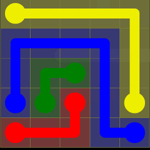
First, I started off with tinkercad. After a short lecture from Dr. Adam Haris I went into tinkerCAD to get a simpler visual of the board I would be creating. This was extremely helpful it allowed me to get a better visual. This is how the board turned out:
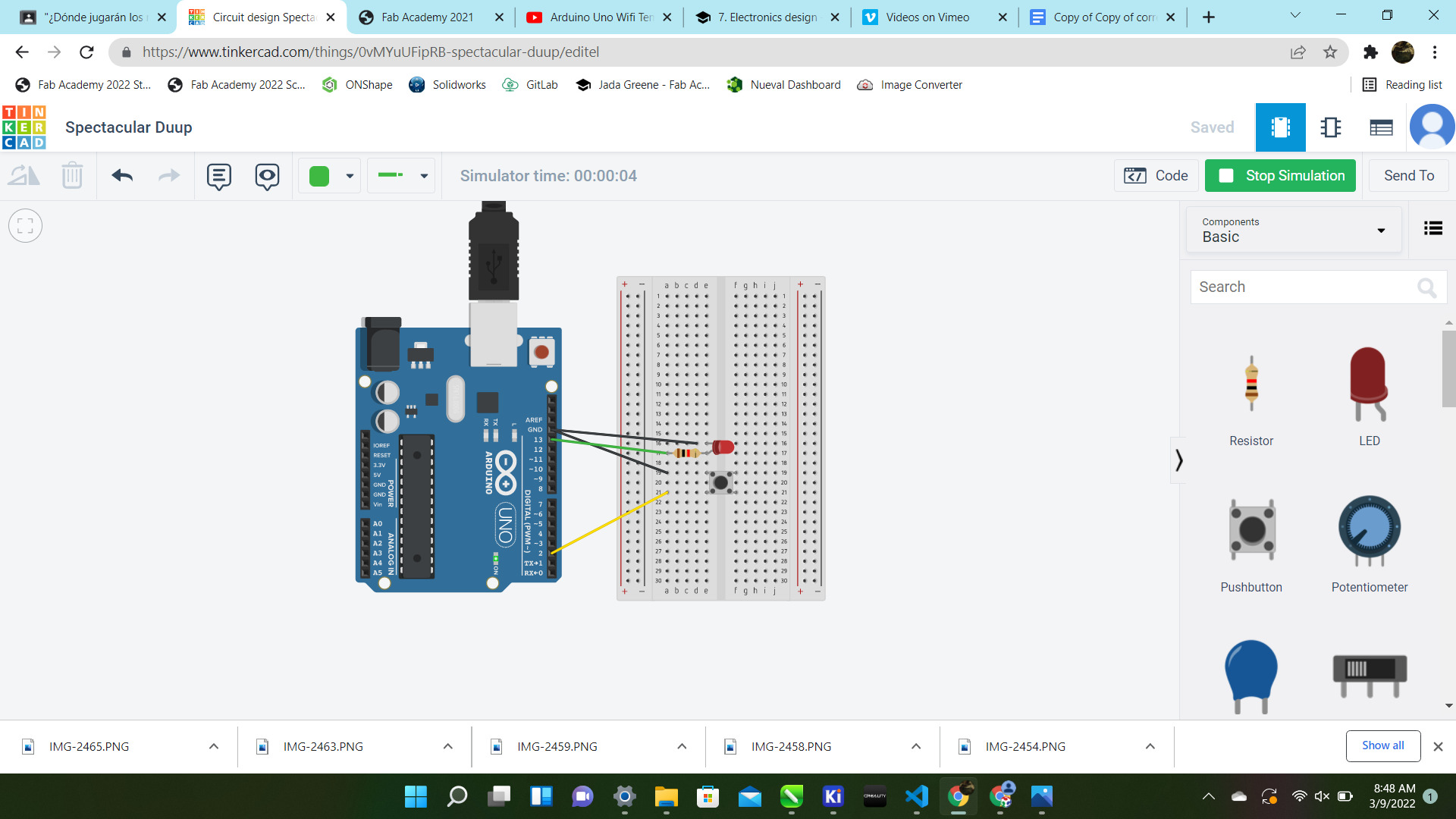
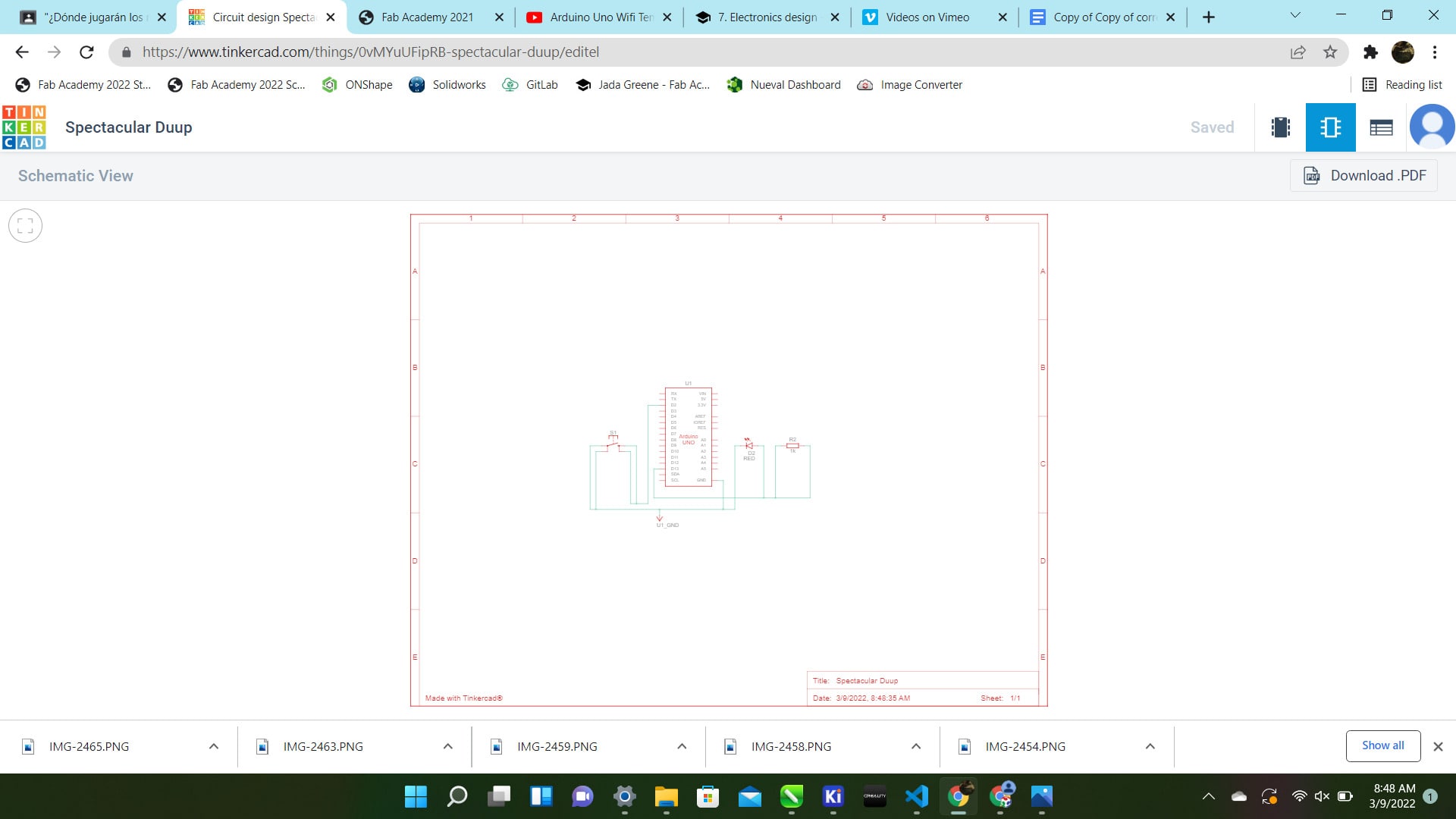
Then tinkerCAD recently made a schematic viewer mode so that was extremely helpful. I am not familiar with schematic but having it in board form really helped my conceptualize what I was going to be creating.
KiCAD
Schematic Editor
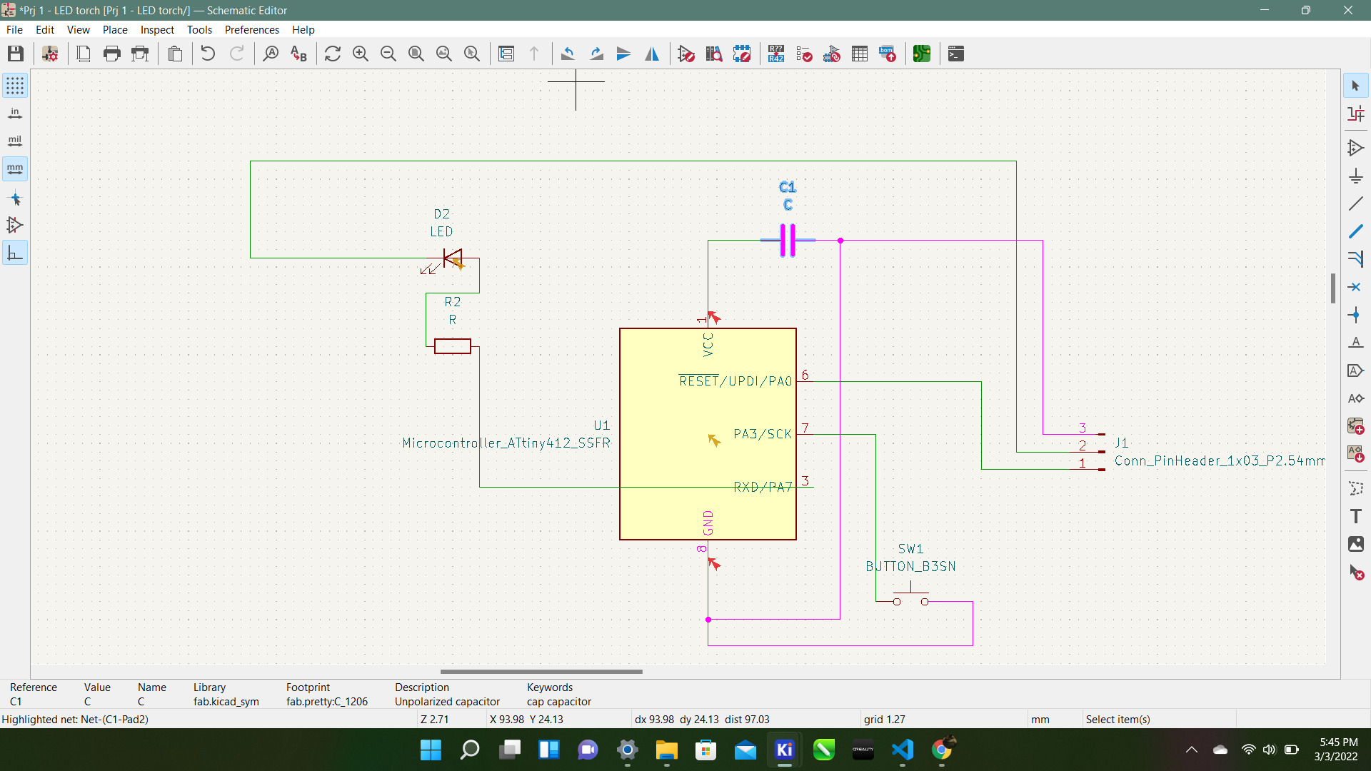
Next, I went downloaded the KiCAD program. Since I am new to this program I used the Tech Explorations videos to help guide me through the process. I used the TinkerCAD schematic as a soft reference image to help me design my schematic. I was trying to design a board with a button that acted as a “pull up switch”. So the LED would stay off unless the button was pressed.
I personally had some trouble modeling it out in KiCAD. I had several different schematic because I continued to get confused on what went where. I also know to have the schematic as easy to read as possible because if the lines are too jumbled up you will get more confused. That is what happened to me. Here is my failed schematic.
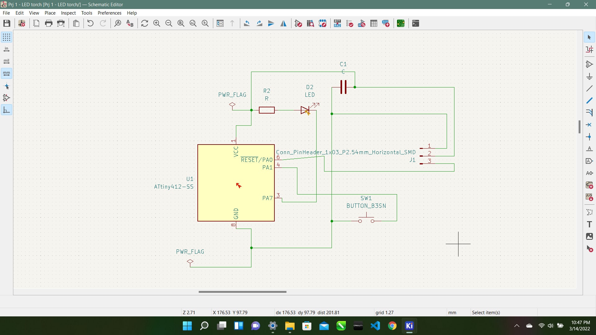
Here is my final schematic design
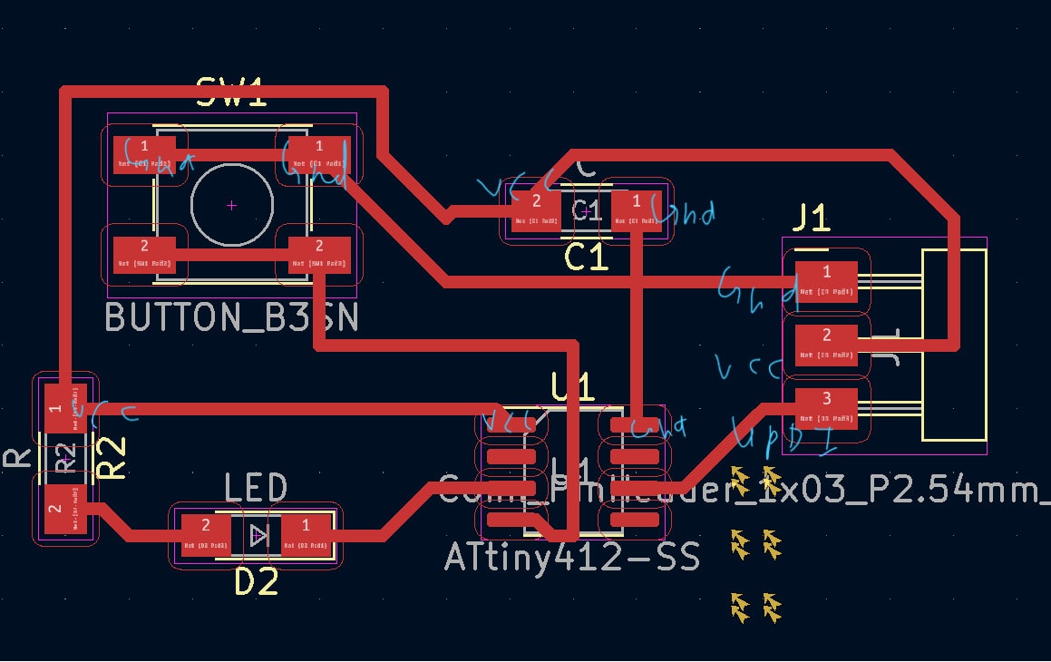
PCB Editor
After I finally figured out the schematic editor and had that set completely I moved on to the PCB editor. The PCB editor was like a game I used to play when I was younger where you had to connect different colored lines withought them touching.
Even though I was good at that game I found this pretty difficult. I always had one that wasn’t connected when I was finished I was very frustrated. I realized I could rotate them so I started to do that and it worked amazing for me. So I did that and finally made a final PCB. Then I used a box to make the edge cut. Also, since I had multiple Schematic I had multiple PCB designs so here they are:
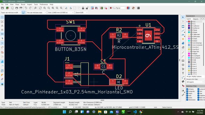
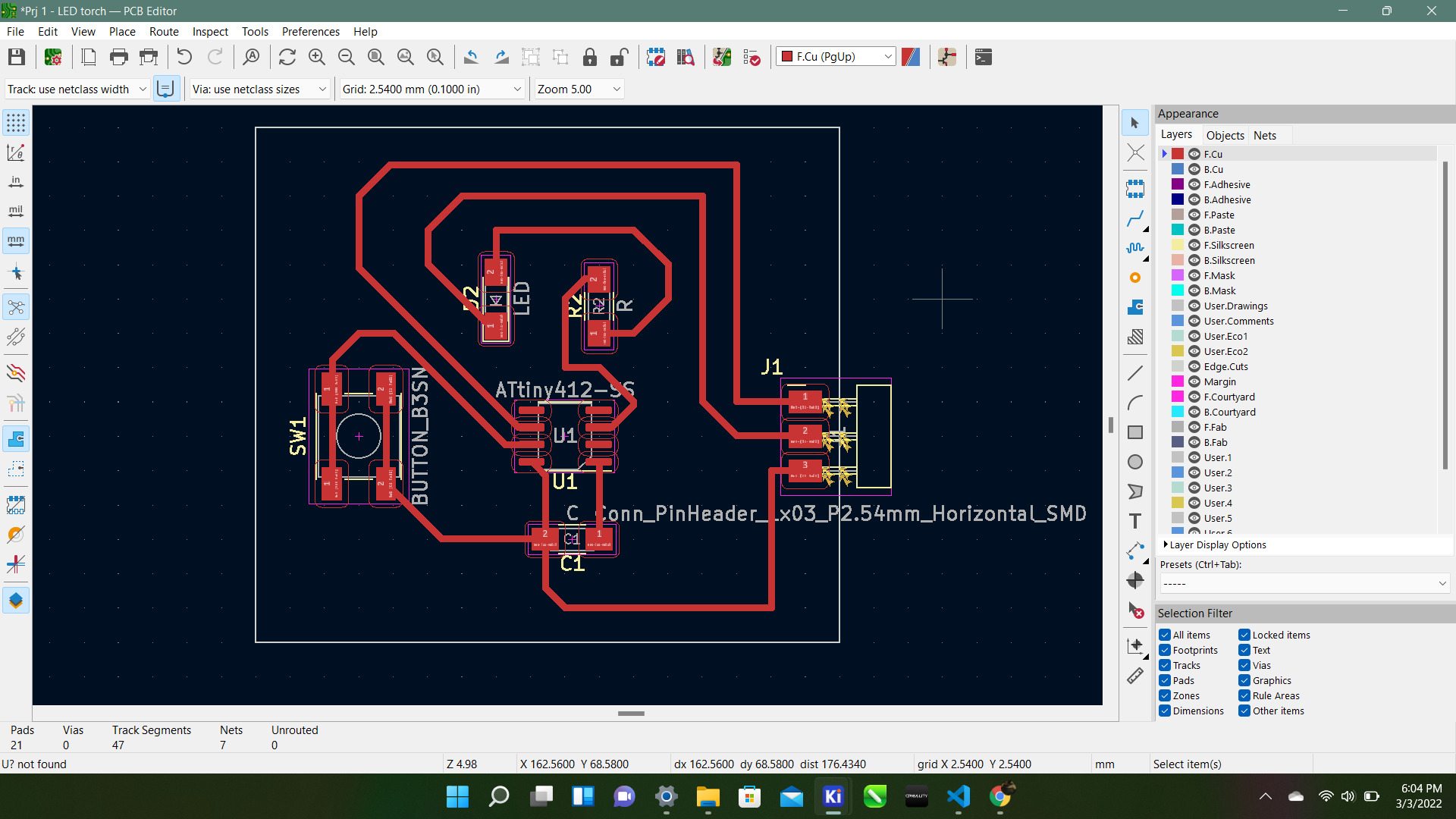
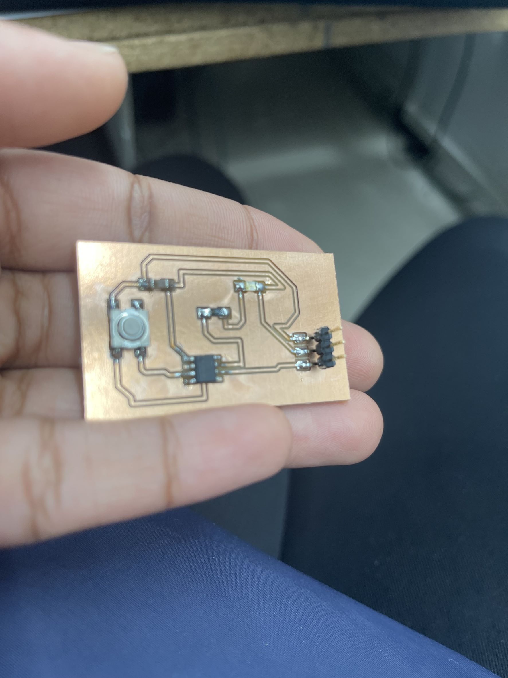
This is the final one I used:
With that design I exported it it out as a Gerber File to be sent to the milling machine. I had to make sure I selected F.Cu and Edge.Cuts layers to be cut. Those and the drill files are the only necessary files needed to mill the board.
Milling
Finally I imported my Gerber files onto the machine I wanted to use and started to mill. I first made the mistake of not referring to the “new” workflow. I came out with these boards which did not work.
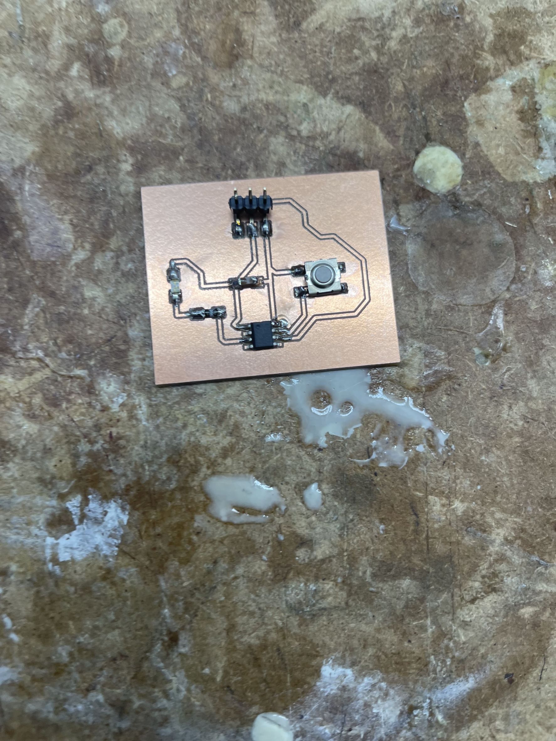
Then finally I reffered to the brand new workflow and got this:
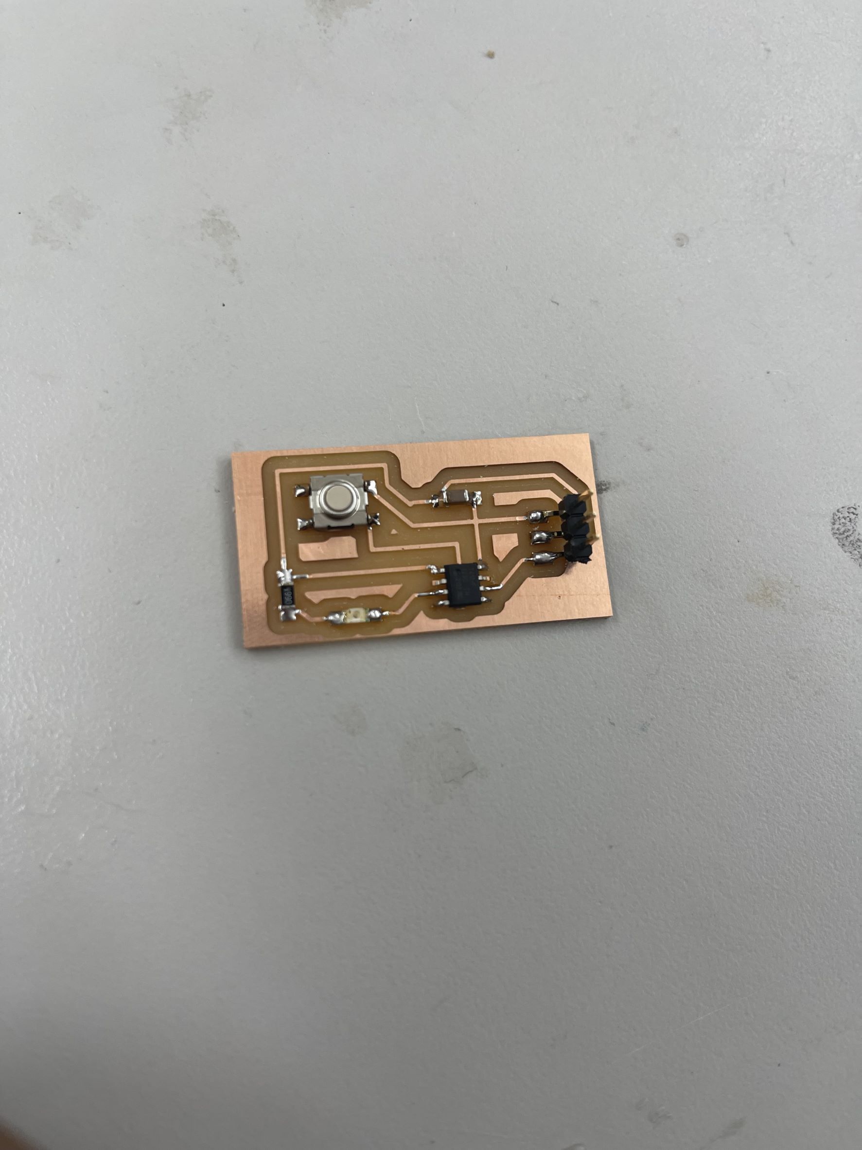
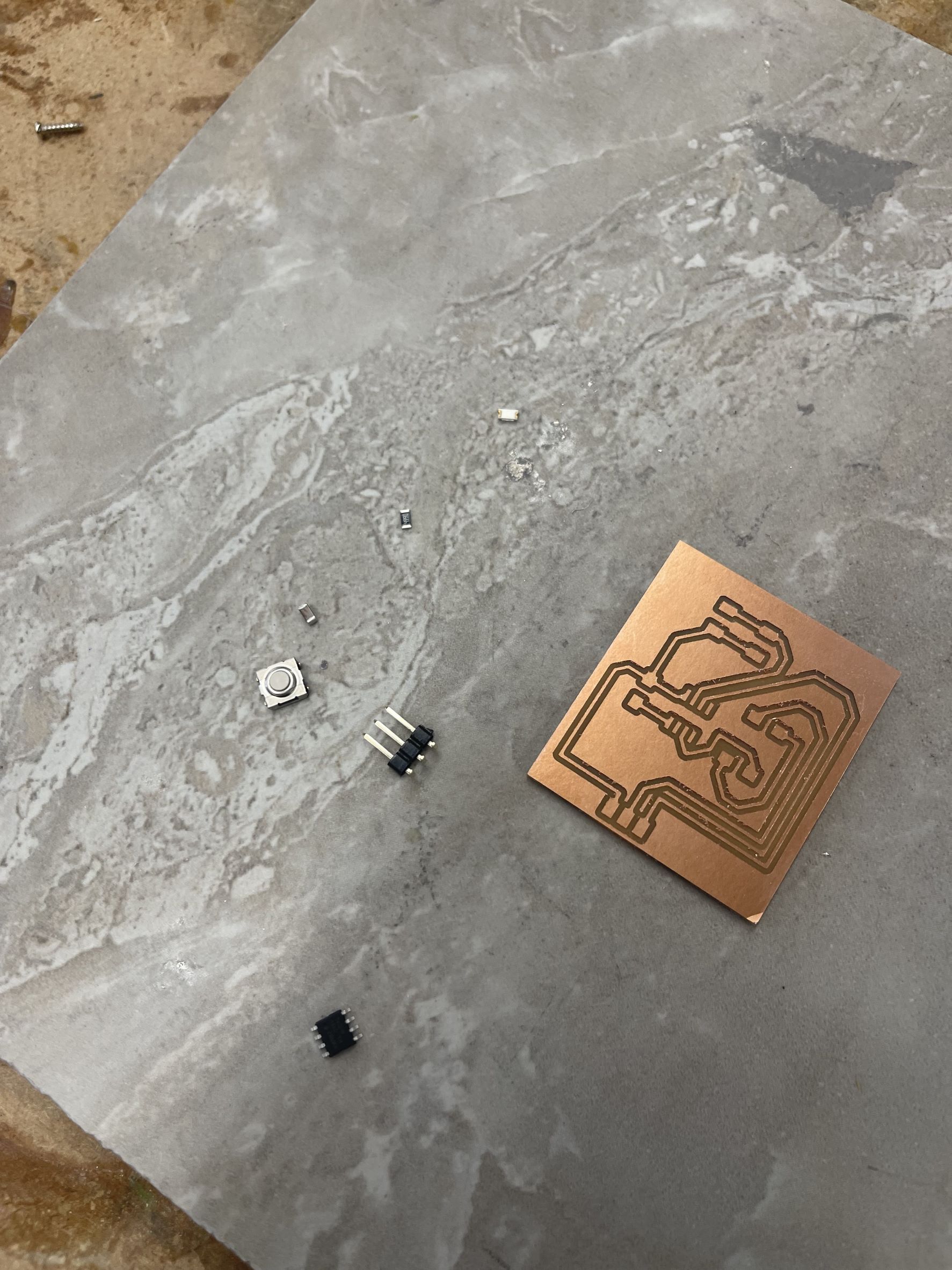
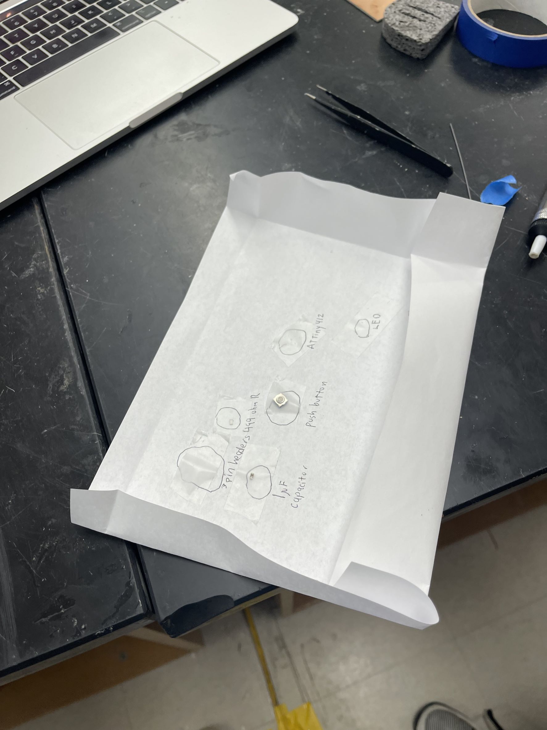
This board was much easier to solder because the trace clearence was 1.5 which was almost double what I was doing before. The components I used were:
-
ATTiny412 chip
-
Unpolarized Capacitor
-
499K Resistor
-
Red LED
-
3 Pin Male Headers
-
4 Pin Button
Programming
I was struggling a lot programming the boards. I have never been very good with programming, so this took me a lot of time to figure out. My previous board have run power and I believe it did not work because the copper was too close and it kept shorting. Although finally with the help of Tom Dubick, we used an arduino to get my board to function.
Specifically, the struggles that I was having were compiling errors and COM errors within the arduino program. I reinstalled the megatiny library. I realized it wasn’t me it was the arduino program so I reinstalled it and that fixed the problem. Next I had a problem with the code. One reason was because the pins were wrong. I did not double check the pin out sheet for the attiny and I had the incorrect pin for my code. Also since my pins were GND to VCC to UPDI it was a little confusing at times. I know now to never do that again. Always have GND and VCC on opposite sides. Then after I fixed the pins we got the code to work! To check we used the standard blink code first.
Here I got the arduino to blink using the standard arduino blink code:
Here is where I got the code specifically to function as a pull up resistor with the button:
Here is the code I used:
void setup() {

  //start serial connection

  Serial.begin(9600);

  //configure pin 2 as an input and enable the internal pull-up resistor

  pinMode(2, INPUT_PULLUP);

  pinMode(4, OUTPUT);

}

void loop() {

  //read the pushbutton value into a variable

  int sensorVal = digitalRead(2);

  //print out the value of the pushbutton

  Serial.println(sensorVal);

  // Keep in mind the pull-up means the pushbutton's logic is inverted. It goes

  // HIGH when it's open, and LOW when it's pressed. Turn on pin 13 when the

  // button's pressed, and off when it's not:

  if (sensorVal == HIGH) {

    digitalWrite(4, LOW);

  } else {

    digitalWrite(4, HIGH);

  }
}
What I Learned
This week I learned how to design a board from scratch using KiCAD. Using the tech explorations videos I plan to take an even deeper dive on KiCAD because I truly enjoyed using that program. I also learned the new workflow and not only how to change the clearence but “why” it is important to. Also through lectures I learned what a pull up and pull down resistor is, I made my board into a pull up resistor.
Group Work
This week the assignment was to test the multimeter and the oscilloscope. I worked on testing the multimeter because I knew how to use an oscilloscope and I havent used a multimeter in a long time. Our work is Here
Design Files
Here are my Design Files for this week: Files