5. Electronics production
Group Assignment:
- Characterize the design rules for your PCB production process
Individual Assignment:
- Make an in-circuit programmer by milling and stuffing the PCB, test it, then optionally try other PCB processes
GROUP ASSIGNMENT
This week I worked on calibrate the CNC Machine so I work with a Circuit Pattern, also I work on the ISP Programmer PCB around the ATiny44 microcontroller.
1. Calibrating the CNC Machine
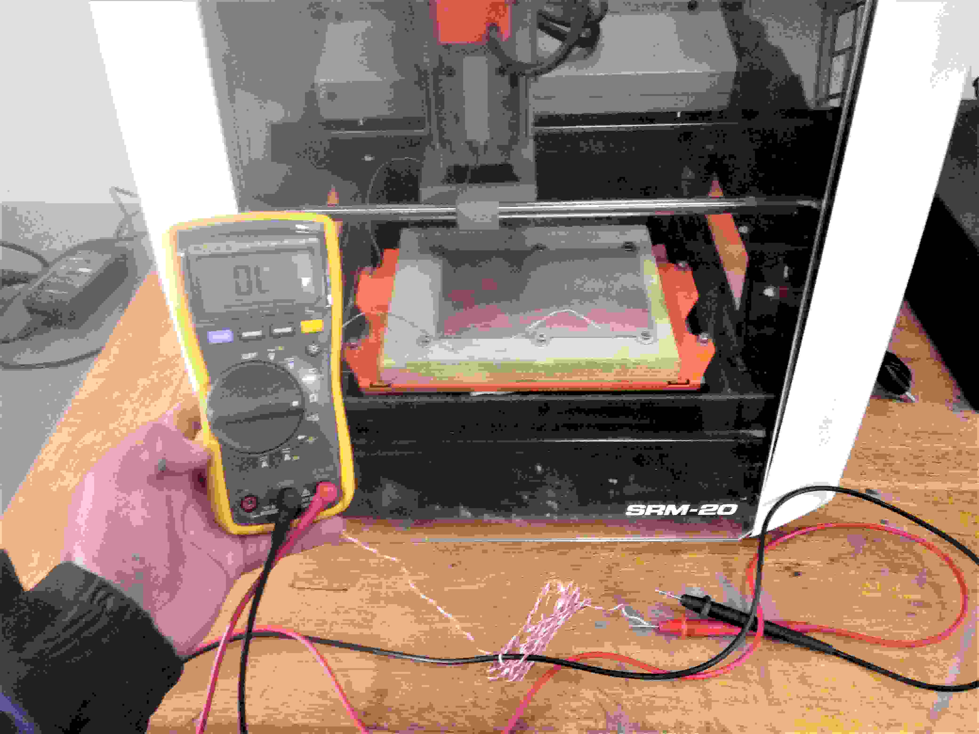
First is necessary calibrate the height of cutting tool of machine, I use a multimeter and wire to check the continuity, and measure the height when the cutting tool touch the PCB
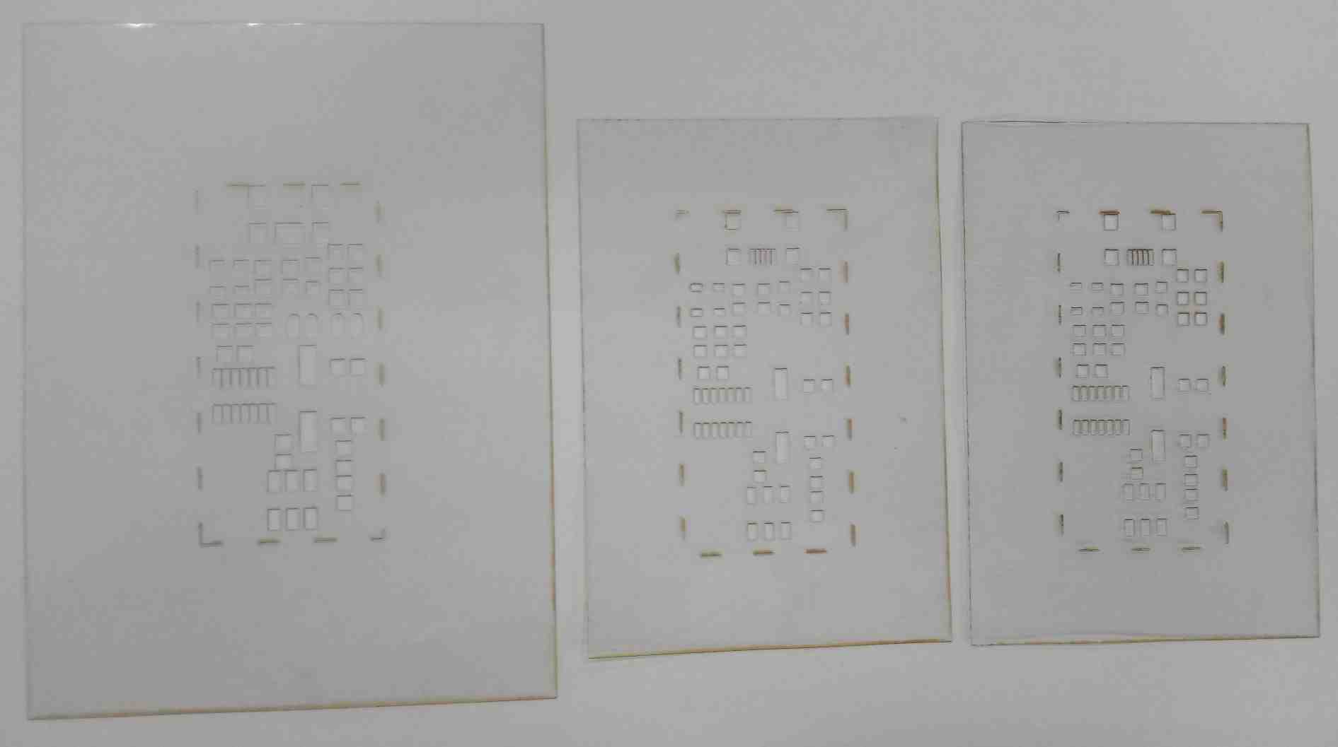
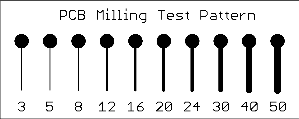
2. Cutting the Pattern Test
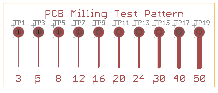
In this work, I design a Schematic of some wire in Autodesk Eagle some wire with diferent width.
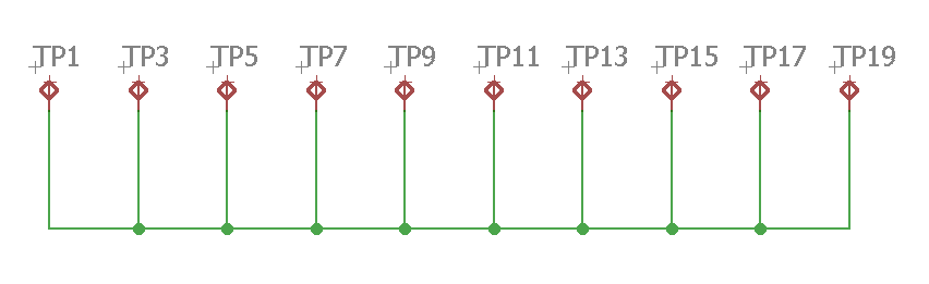
After, I design the PCB of the Pattern Test with different width of wires, from 3 mills until 50 mills
To work in Fabmodules tools I need export the PCB design in monochrome image and high resolution, so I use the follonig parameters in export option in Autodesk Eagle:
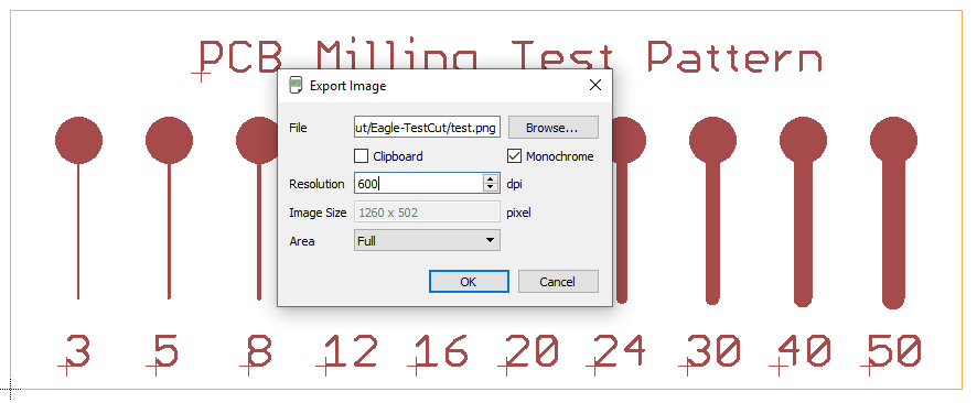
The monochrome image has only two colors, black and write, you can see in the picture:

So I use in fabmodules.org
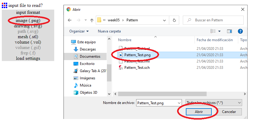
I open internet explorer and load the image PNG format, I select the file and press ACCEPT button to load:
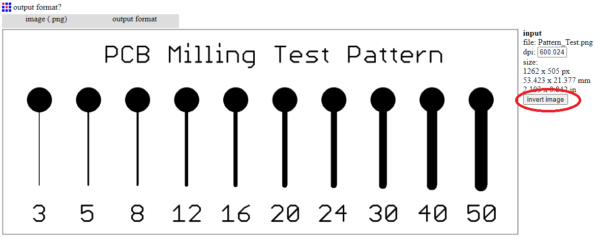
I must invert the image color because the white part is validated part:
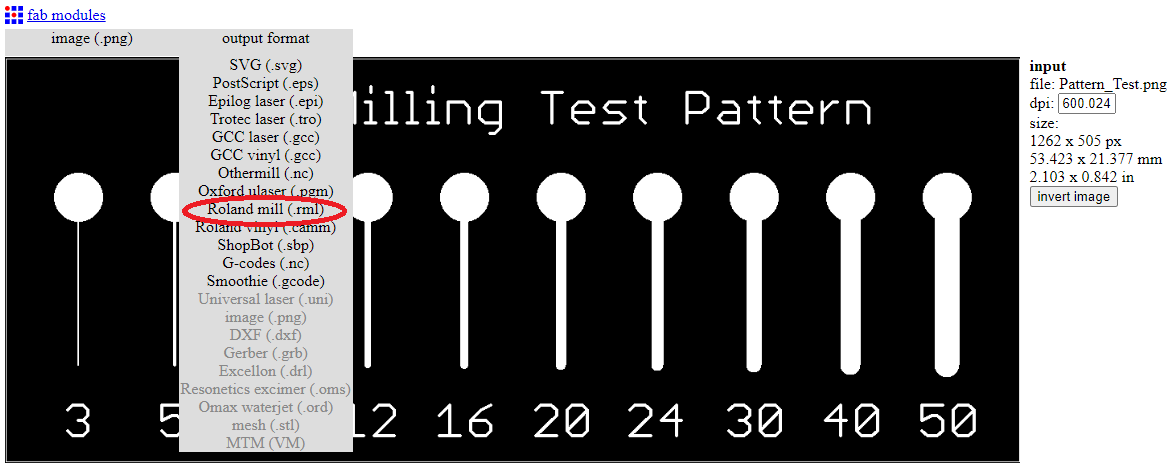
Now, I choose the output format to ROLAND MILL because I use the MONOFAB SRM-20 from ROLAND company:
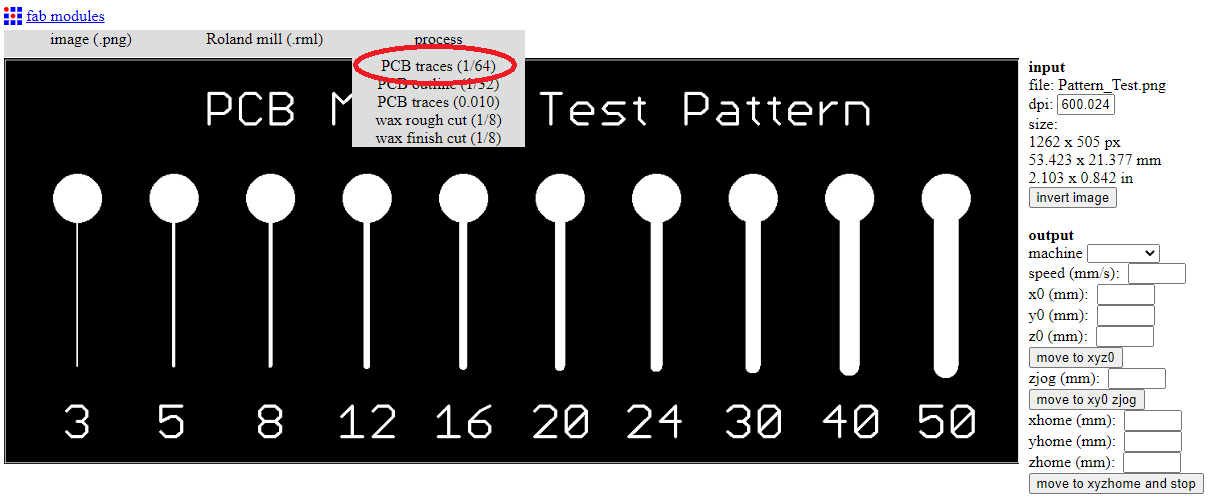
Afterwards, I choose the process to PCB traces (1/64) because it is the format to MONOFAB machine:
Now, I configurate the parameter to work the traces of the PCB:
    Machines = SRM-20
    x0 = 0
    y0 = 0
    z0 = 0
    cut depth (mm) = 0.025 mm
    tool diameter (mm)= 0.2 mm
    number of offset = 1
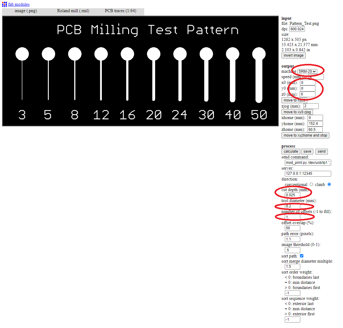
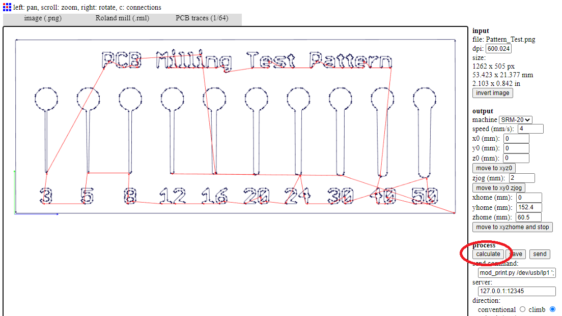
Then I press the CALCULATE button to calculate the cutting trajectory, and I press the SAVE button to save the MONOFAB’s files, it load to the machine:
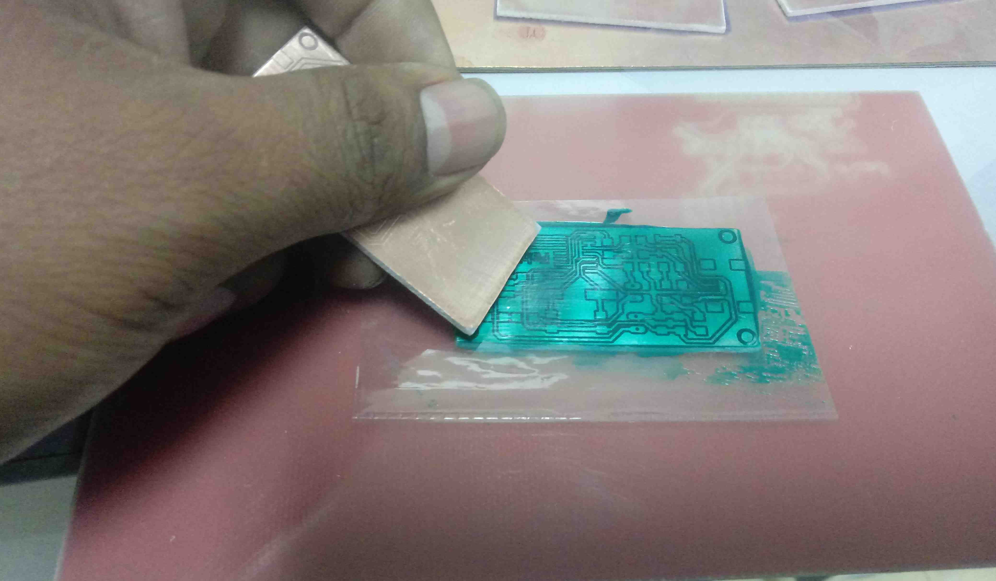
The process cutting is similar to the INDIVIDUAL ASSIGNMENT, this part you can see there; the cutting of the Pattern Test is done:
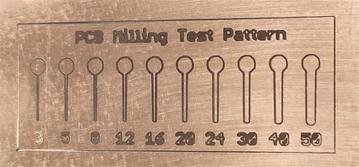
We test the copper tracks that were cut to make a comparison with the size it should have:
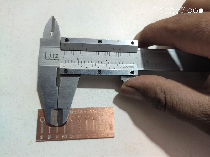
Measurements were made on all generated tracks
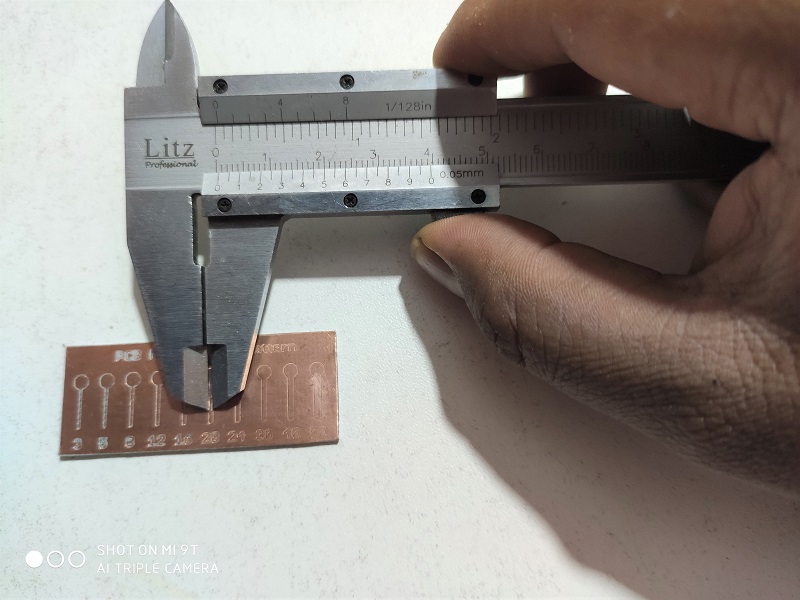
To calculate the measurements in mm, convert them into mils or thousandths of an inch we have the following formula:
mils = mm x 1000 / 25.4
The result of the measurements and conversions is the following table:
| Item | Measures (mm) | Converted (mils) | Reference (mils) | Error (%) |
|---|---|---|---|---|
| 1 | 0.00 mm | 0.00 mils | 3 mils | - 100 % |
| 2 | 0.20 mm | 7.87 mils | 5 mils | + 57 % |
| 3 | 0.25 mm | 9.84 mils | 8 mils | + 23 % |
| 4 | 0.40 mm | 15.74 mils | 12 mils | + 31 % |
| 5 | 0.50 mm | 19.68 mils | 16 mils | + 23 % |
| 6 | 0.60 mm | 23.62 mils | 20 mils | + 18 % |
| 7 | 0.75 mm | 29.52 mils | 24 mils | + 23 % |
| 8 | 0.90 mm | 35.43 mils | 30 mils | + 18 % |
| 9 | 1.05 mm | 41.33 mils | 40 mils | + 3 % |
| 10 | 1.35 mm | 53.14 mils | 50 mils | + 6 % |
INDIVIDUAL ASSIGNMENT
1. Design the PCB
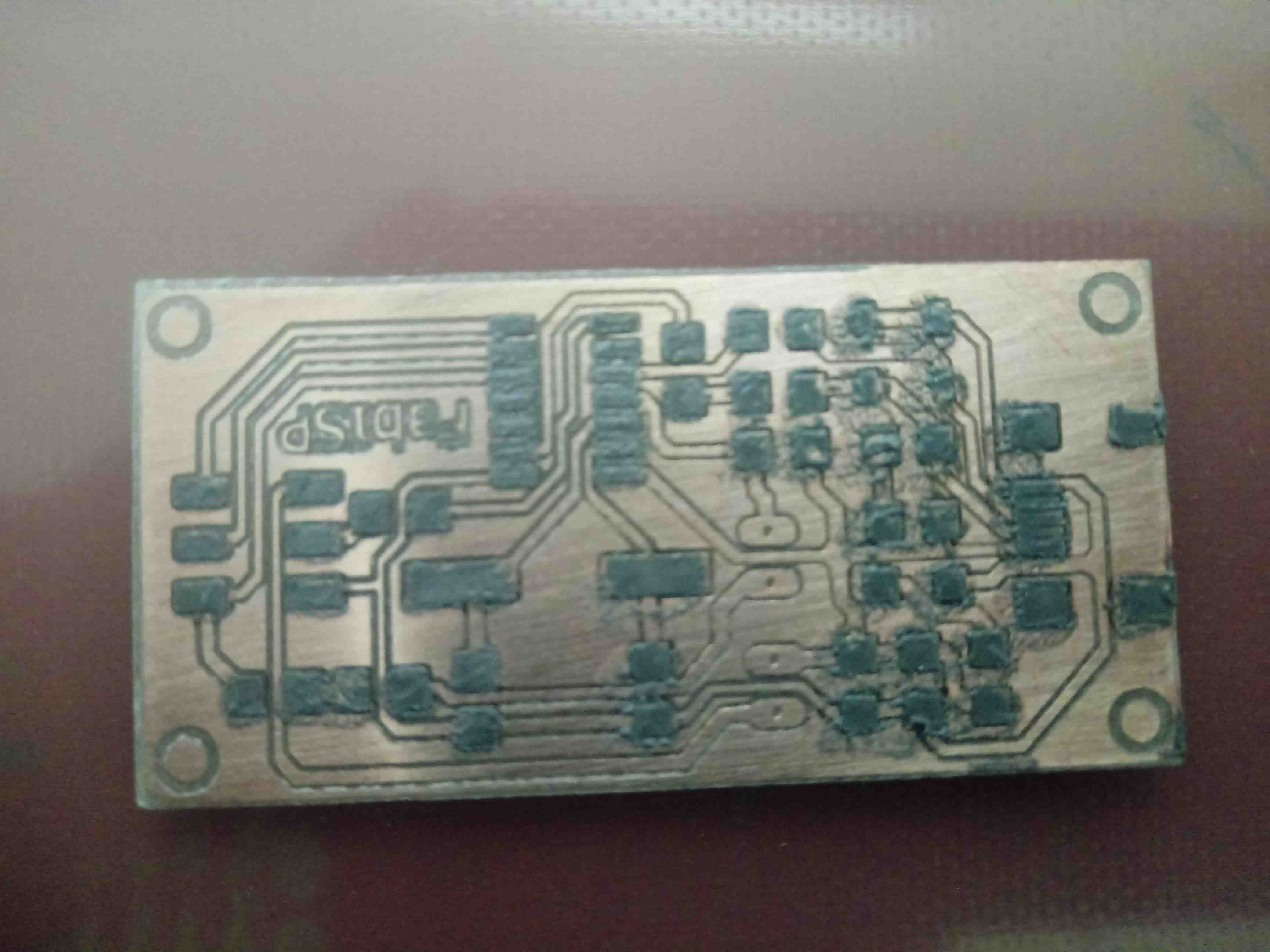
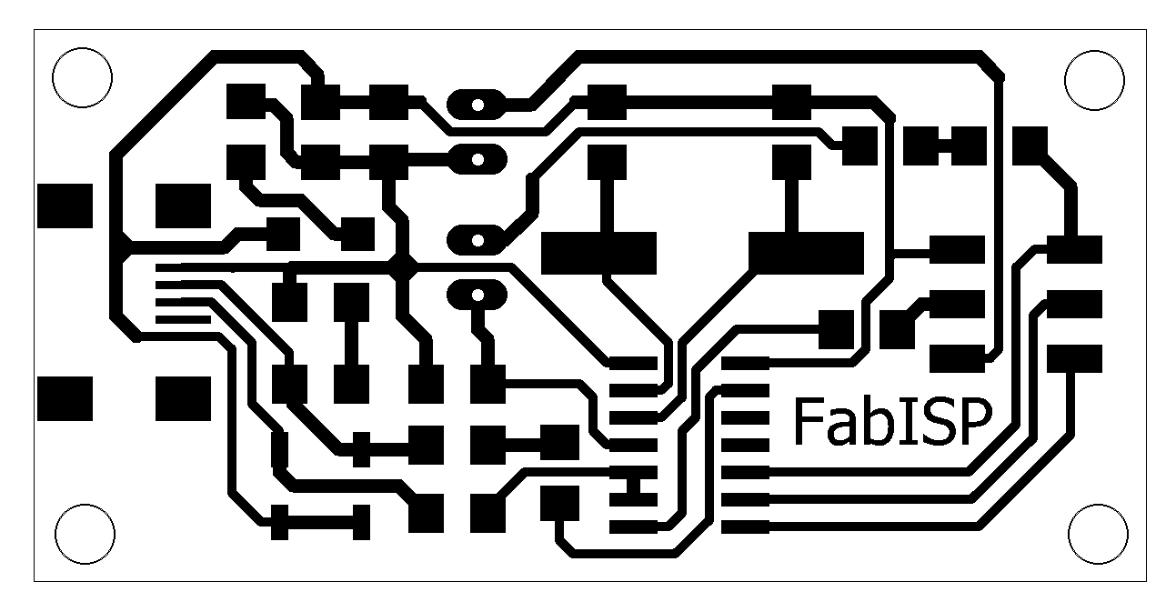
For the manufactured FABISP I used the Archived Design in FABACADEMY, I changed the design because I want to improve it and make it smaller and more portable
First I design in Autodesk Eagle the Schematic and the PCB
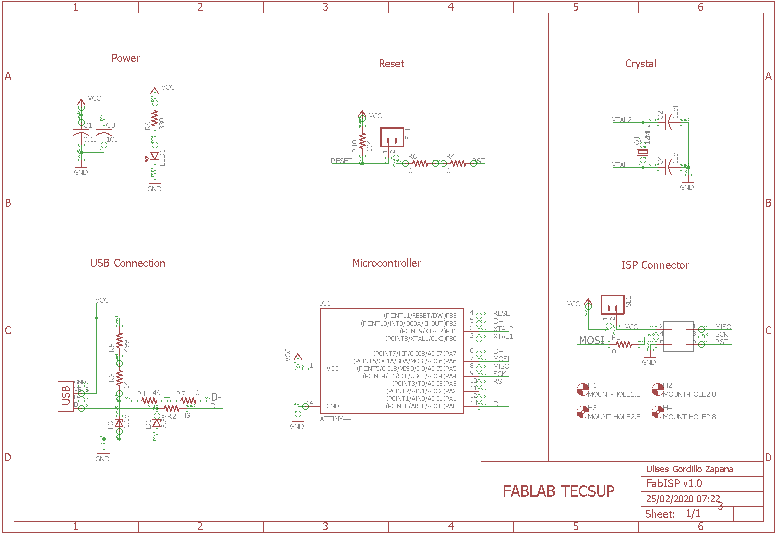
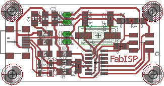
I design the PCB on the Bottom layer:
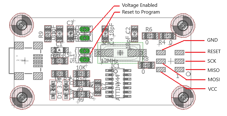
Define the description of the Pinout:
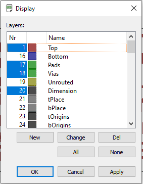
To export the image for the cutting machine, We need select the correct layer:
The image should look like:

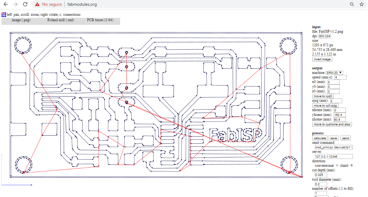
Then we process the design with fabmodules’s web:
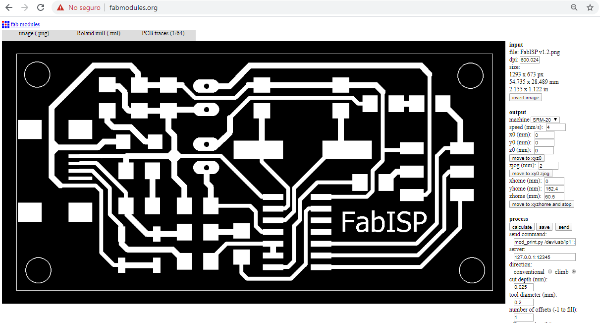
Fabmodules’s web calculates the trayectory of the cutting machine:
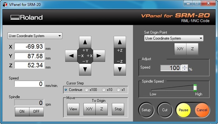
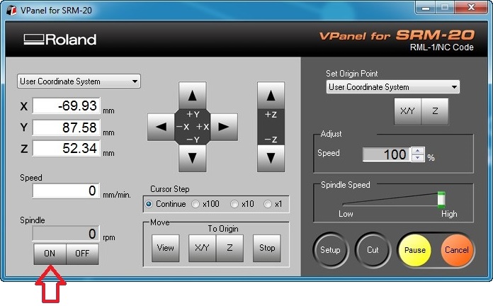
Open the VPanel Software, it control the Monofab SRM-20 machine:

Calibrating the initial position of work:
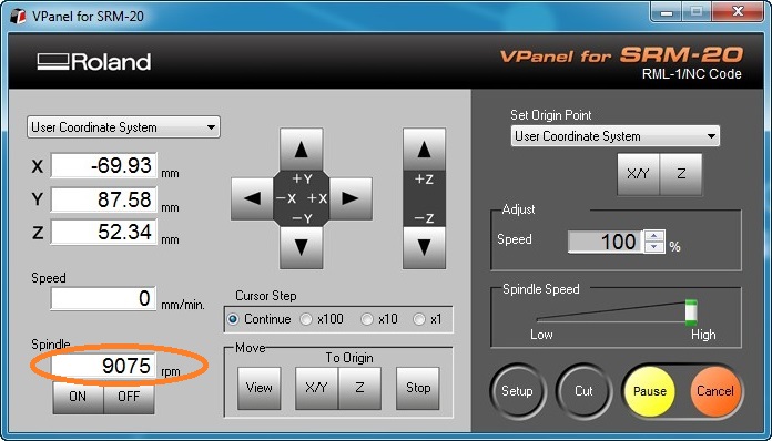
Turn ON the spindle of the Monofab:
Wait the starting of the spindle until the upper 8000 RPM:
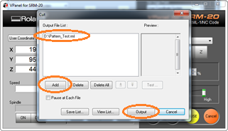
Preparate and load the cutting file in the button CUT:

Load the file and OUTPUT to cut the design:
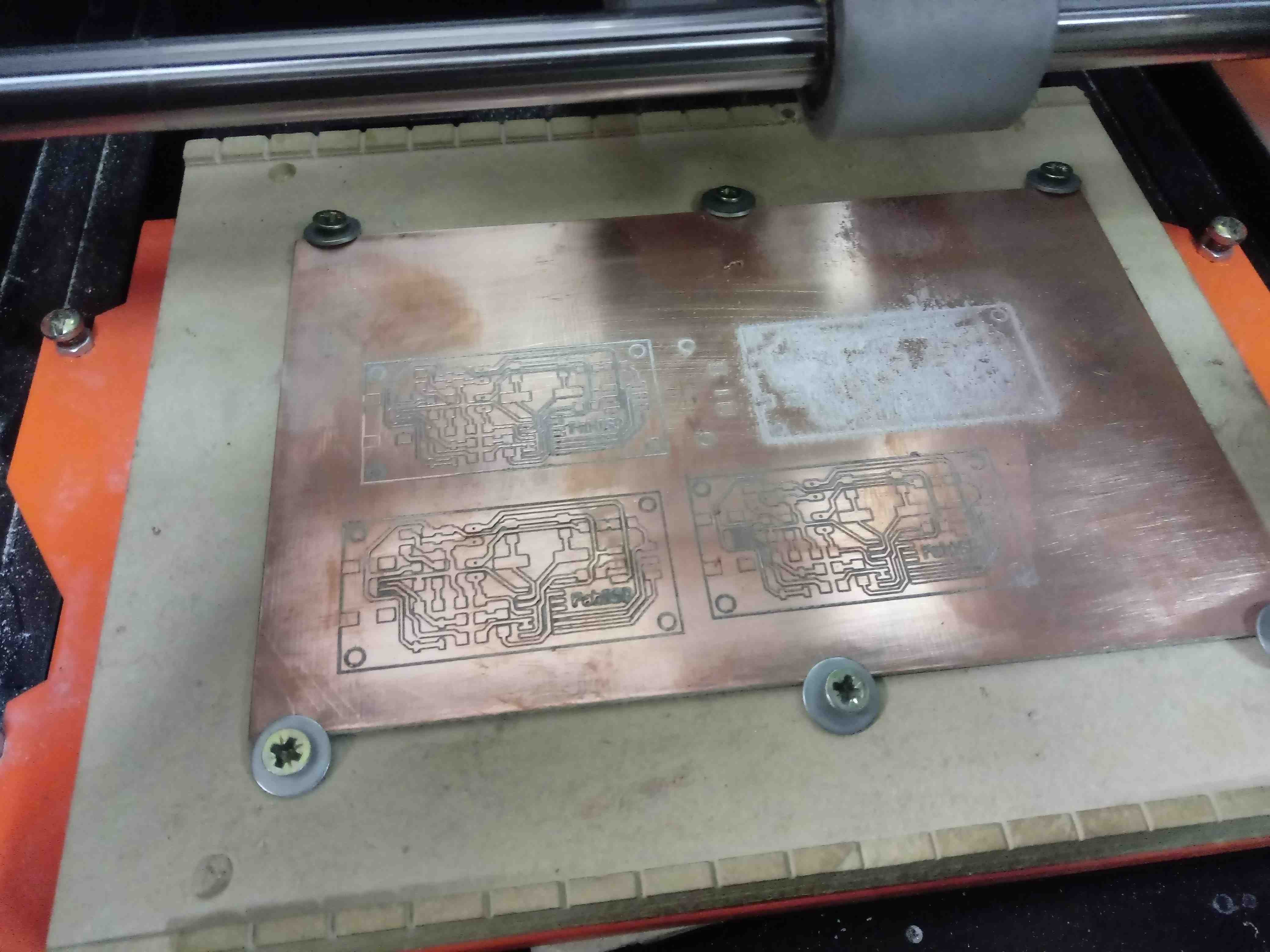
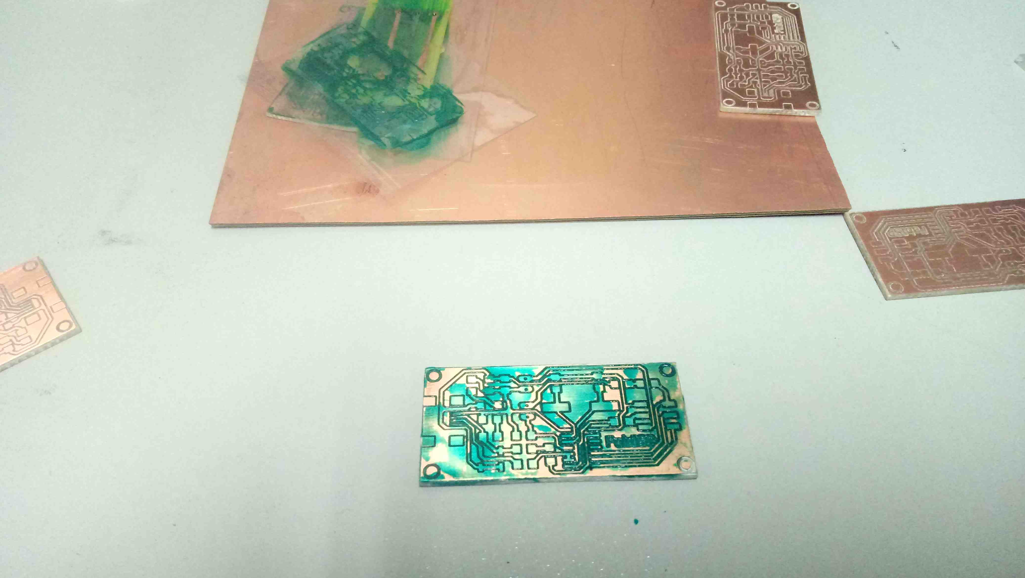
We can see the process:
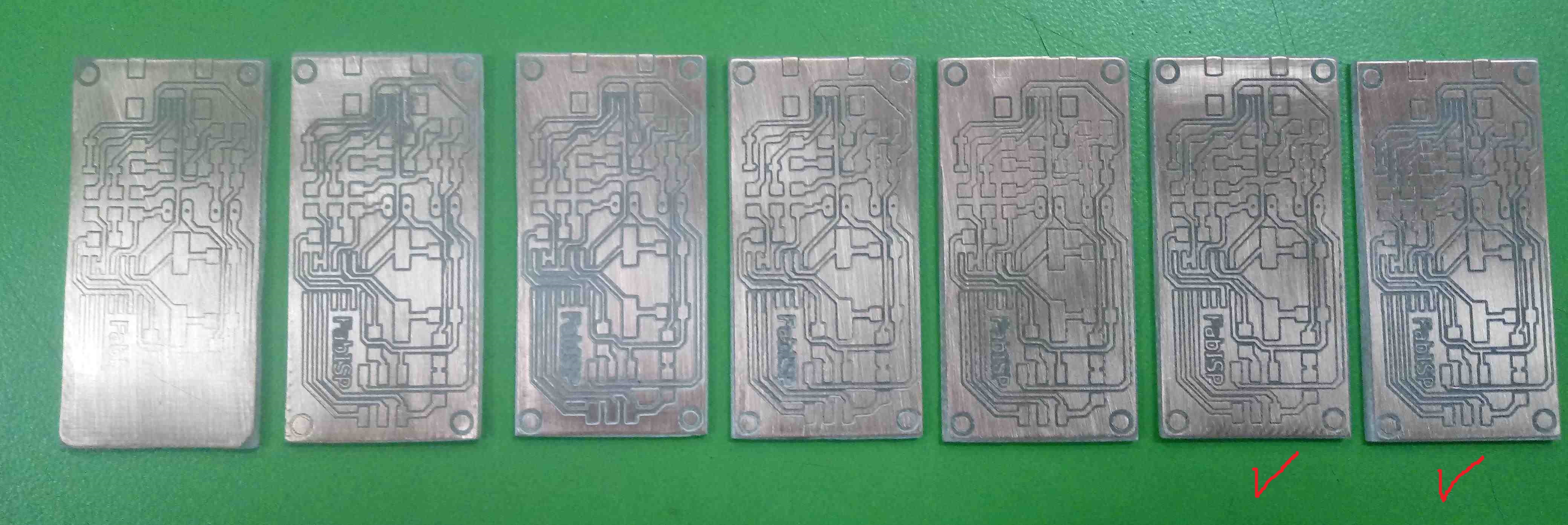
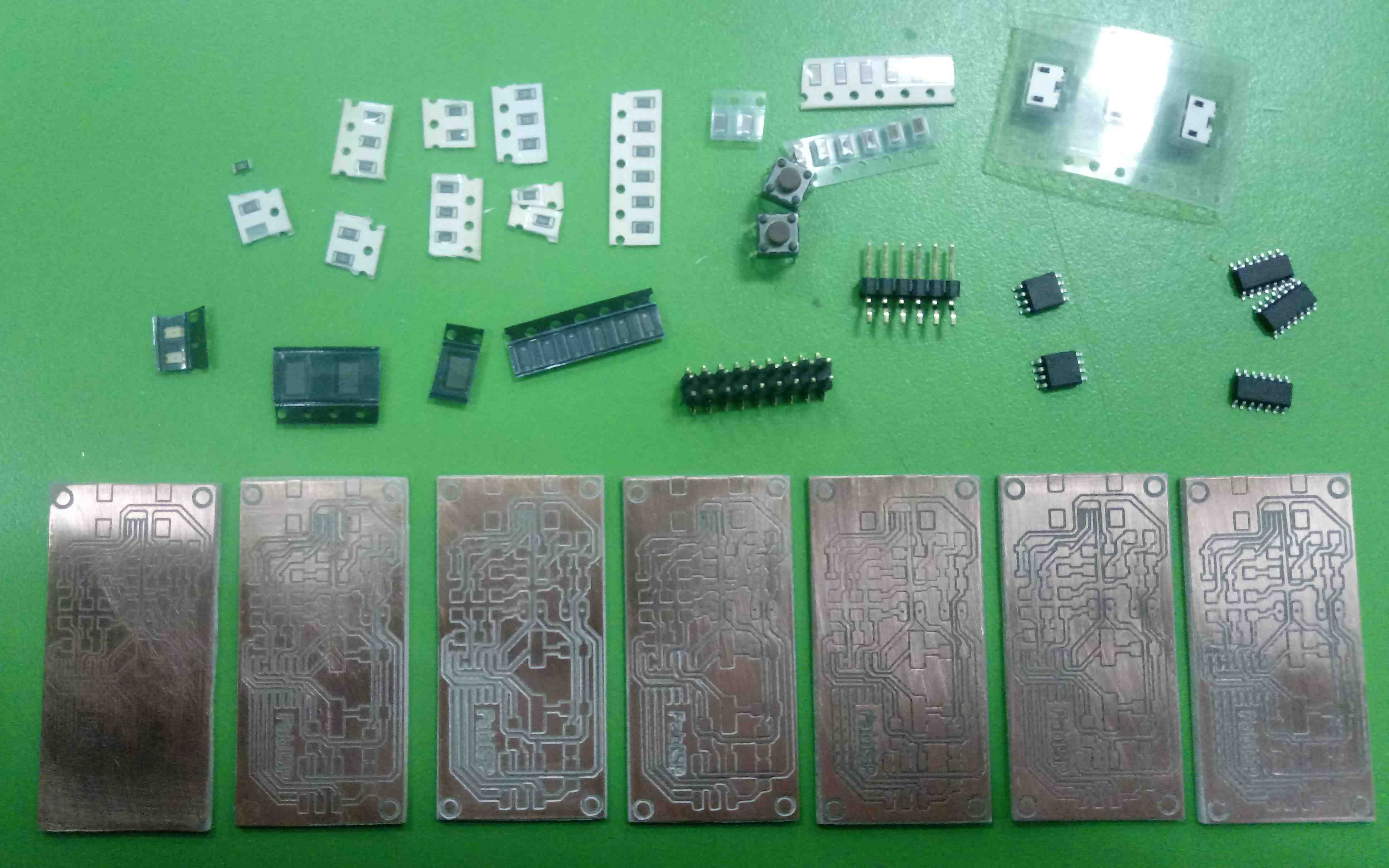
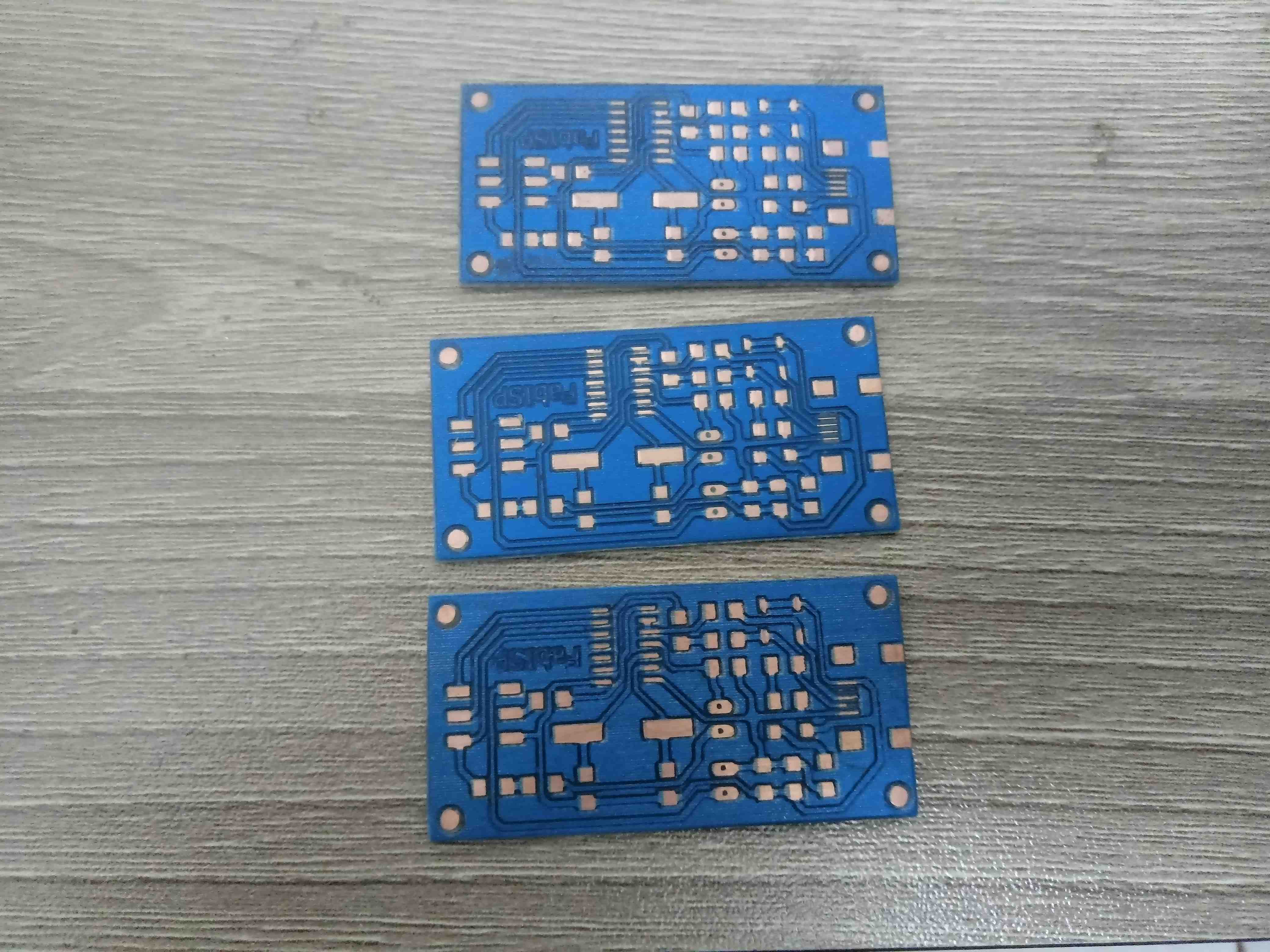
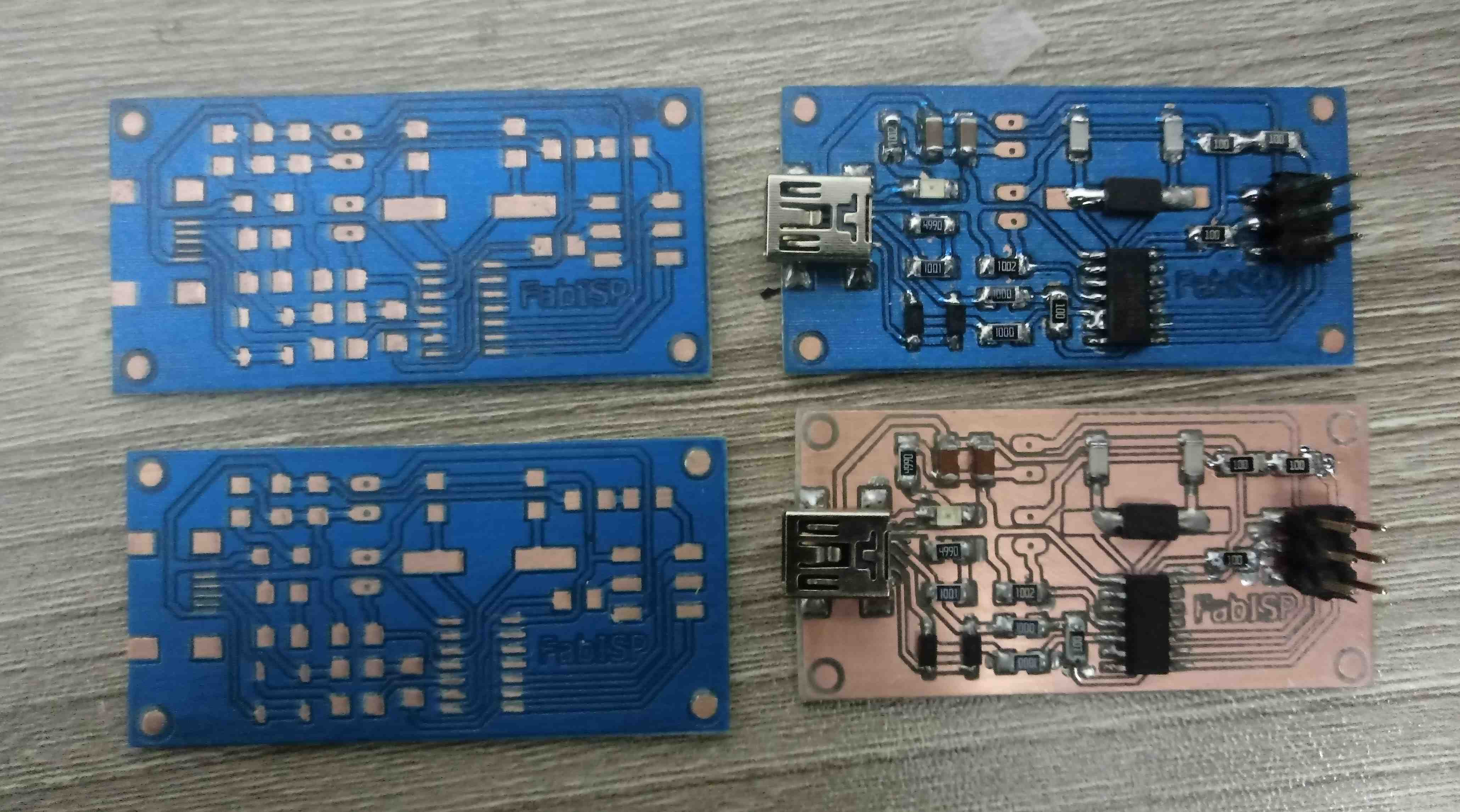
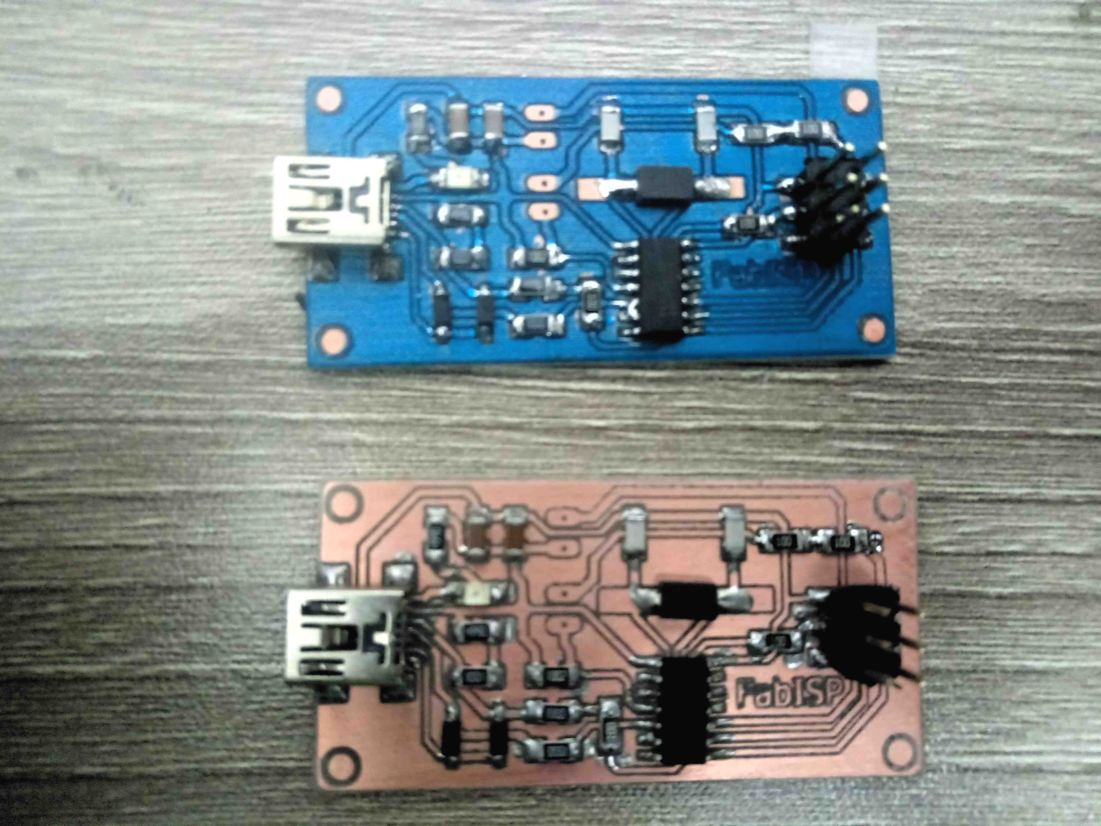
We fabricate the PCBs:
I have some samples, I will choose the best two; one to work without an anti-solder mask and the other I will print an anti-solder mask on a UV printer:
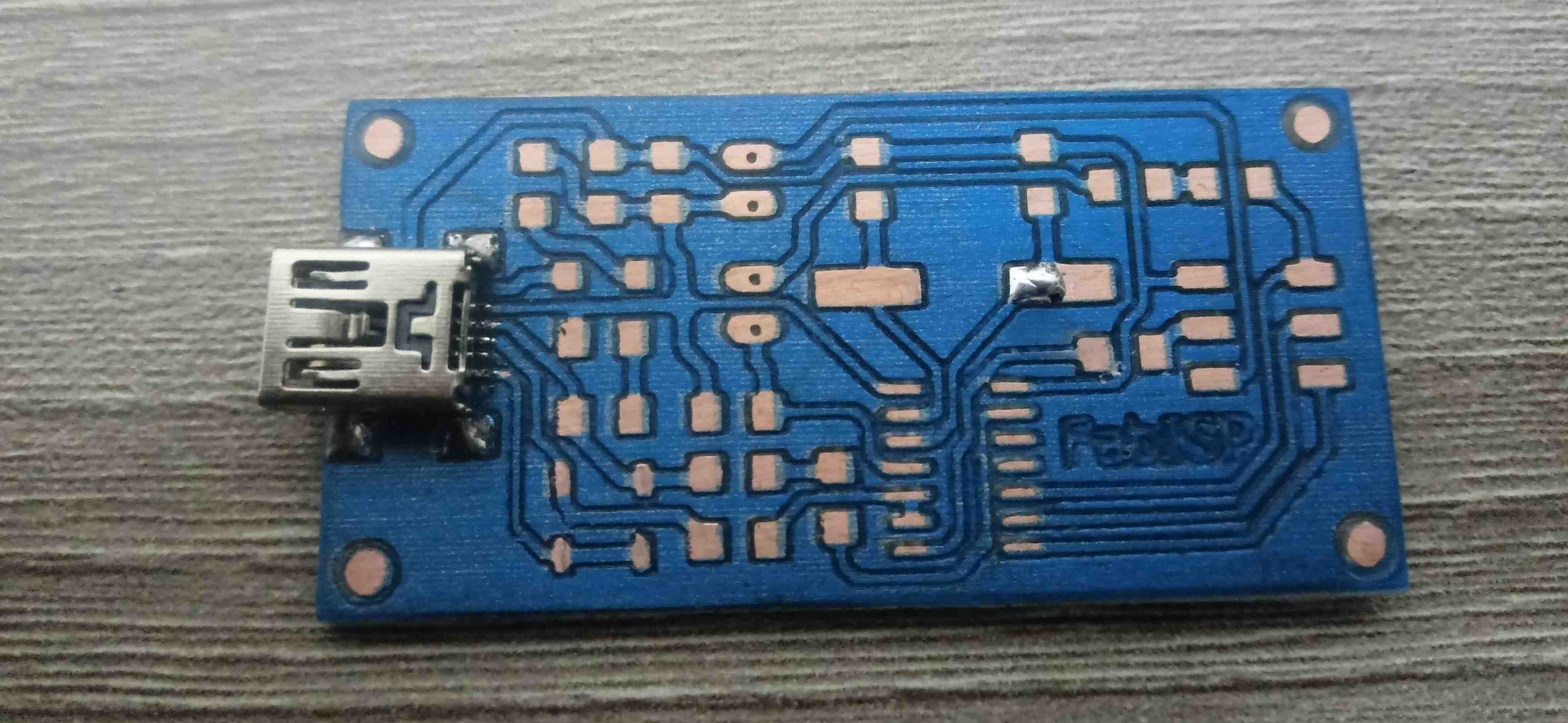
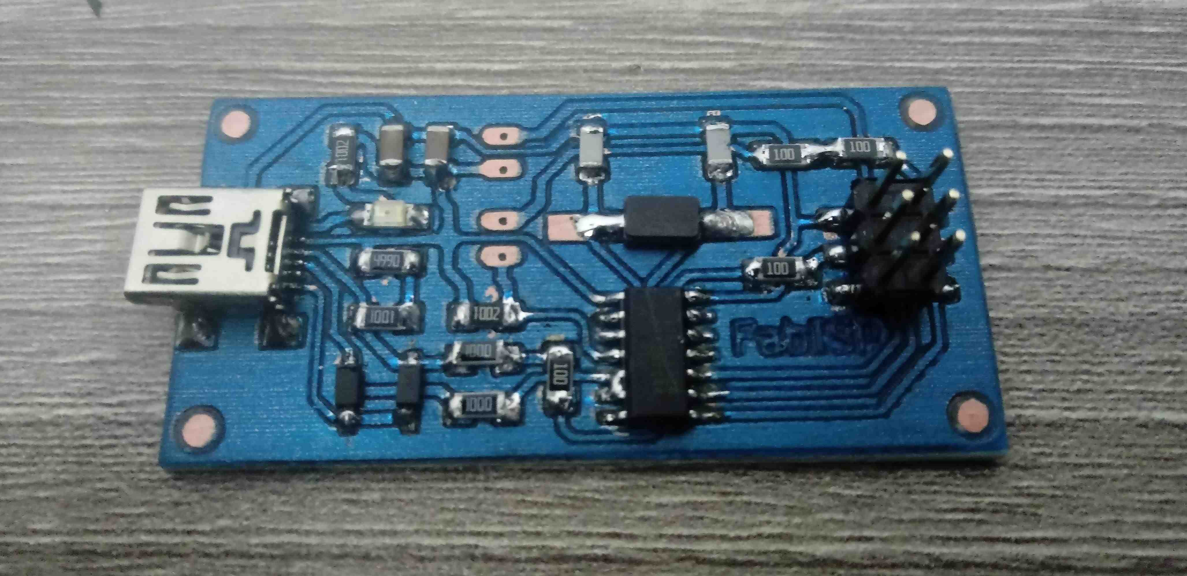
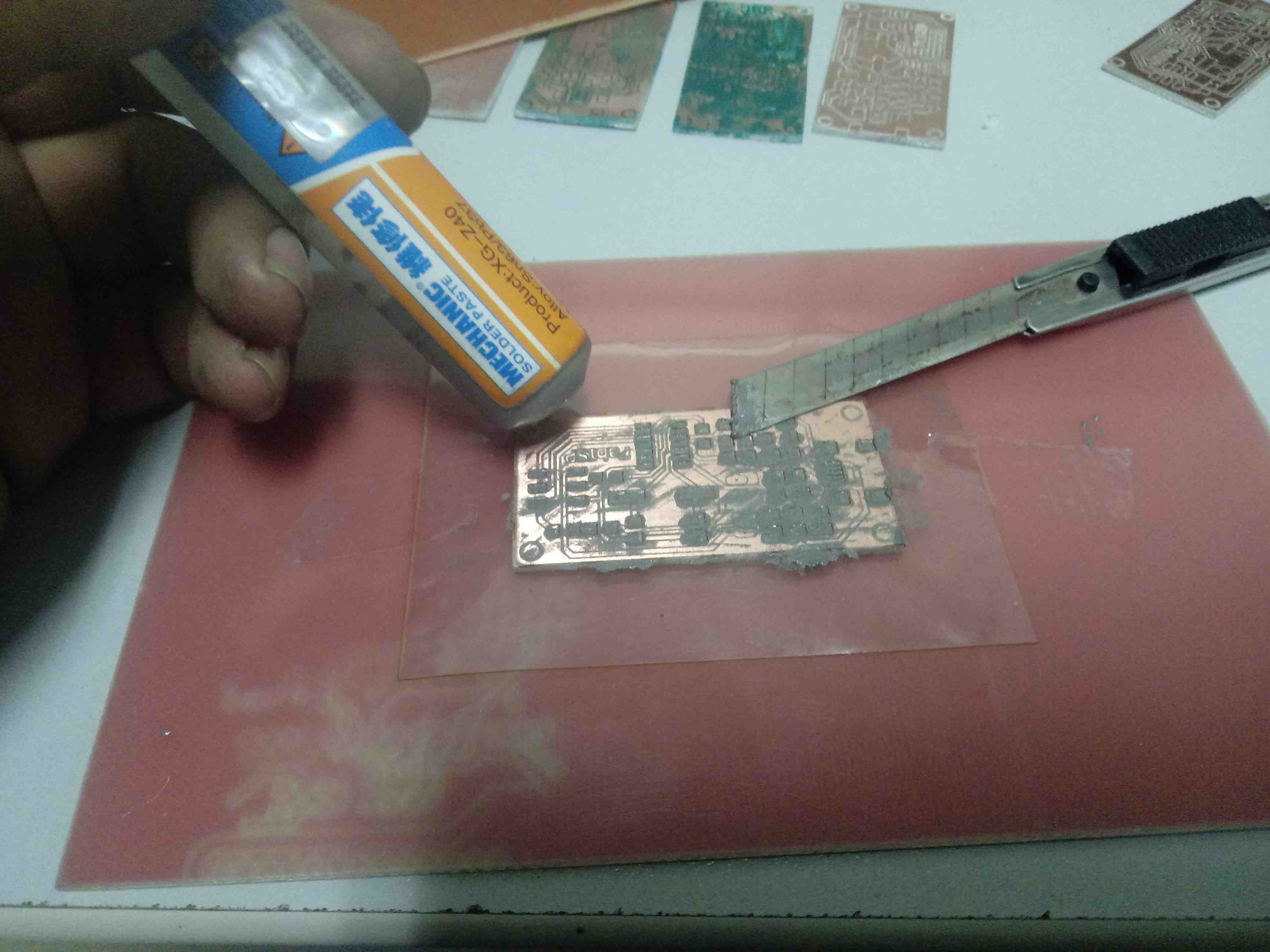
2. Soldering the PCB without anti-solder mask
I preparate the SMD electronic component:
I started to weld from the smallest component, which in this case are the resistors, capacitors and LEDs; then I install the integrated and finally the connectors
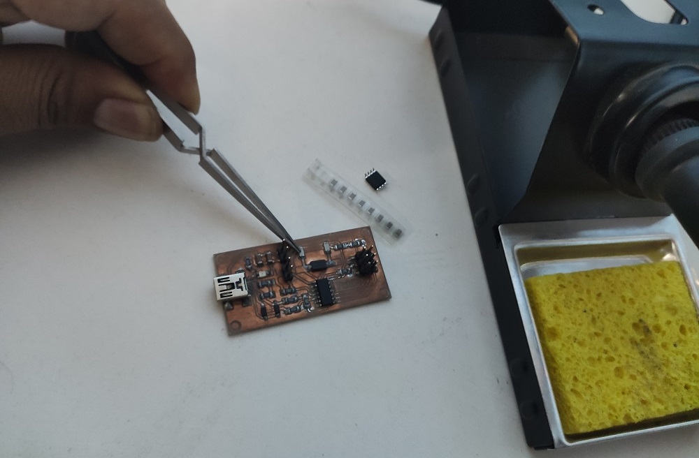
A tip to make a good solder is to start with placing a little tin on a pad then solder the pad with the component helping me with an internal pressure clamp, because it makes the process much easier.
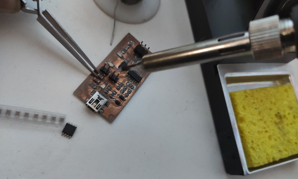
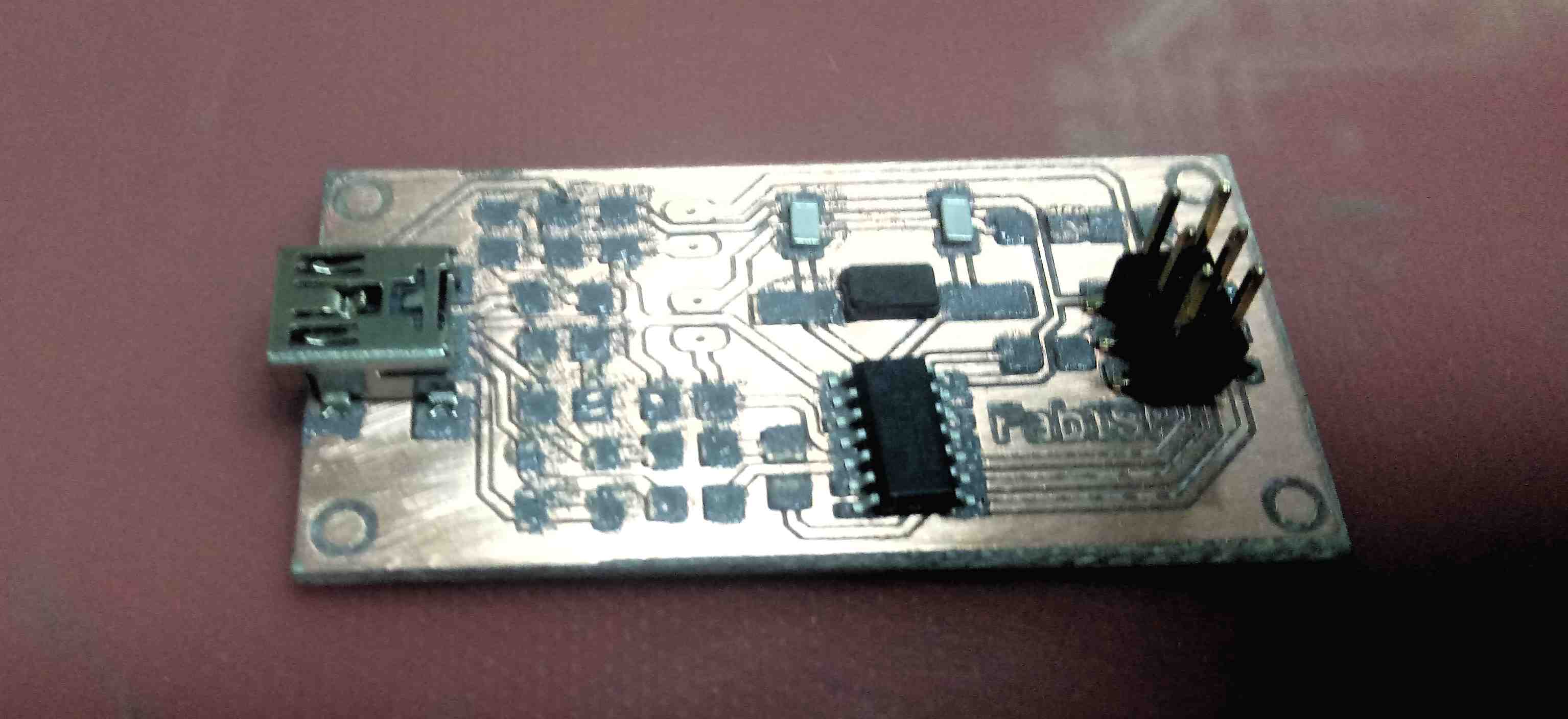
Finally the welded plate ends this way:
3. Programming Firmware
For the programming of the FABISP I must pay attention to programming the firmware and the fuses:
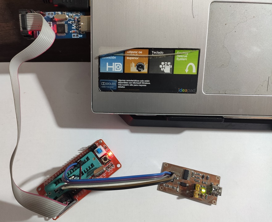
I use the USPASP programmer to load the firmware to FABISP board
I installed the eXtreme Burner Software to install the firmware in the microcontroller
When The Extreme Burner Software is loaded, I choose in Chip->Attiny44; it is to work with this micontroller:
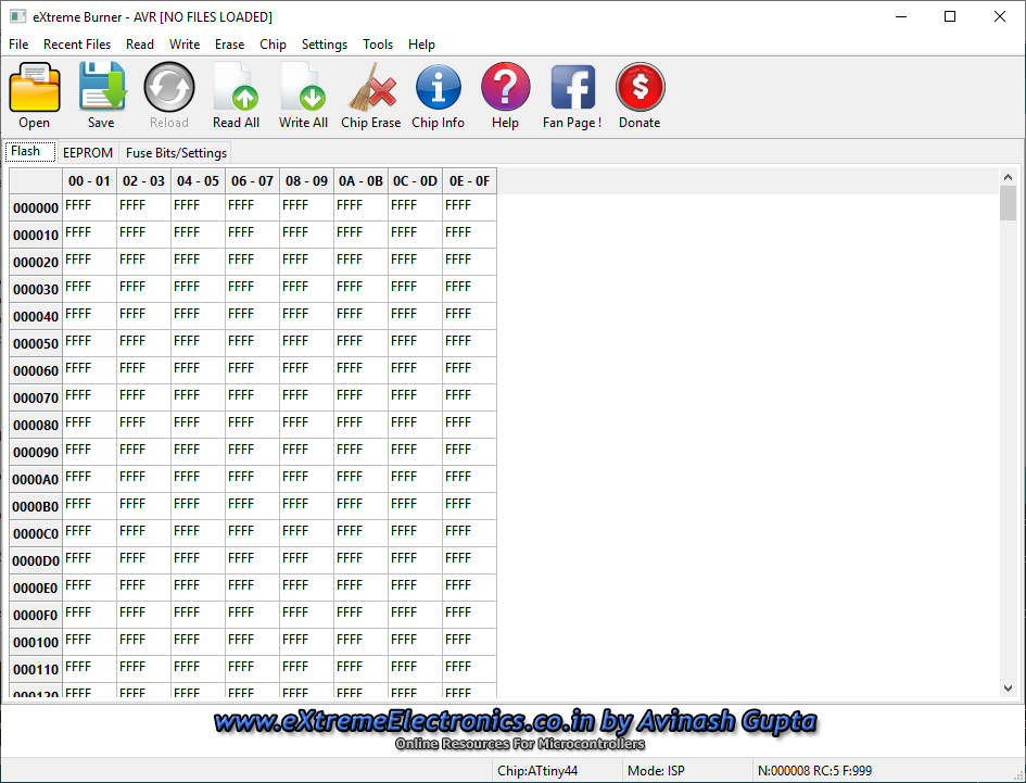
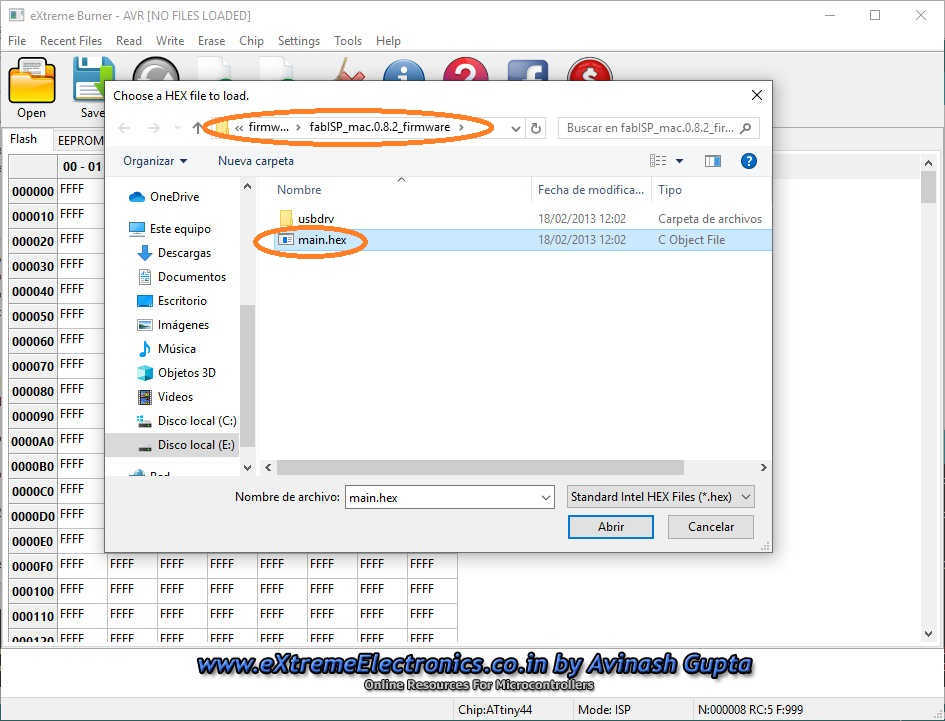
Afterwards, I choose the load option in File->Open Flash; it is to load the firmware to Attiny44; I explore the file to firmware path:
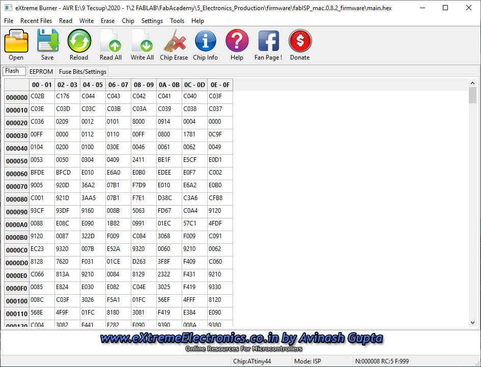
The firmware is loaded, and you can see in the picture:
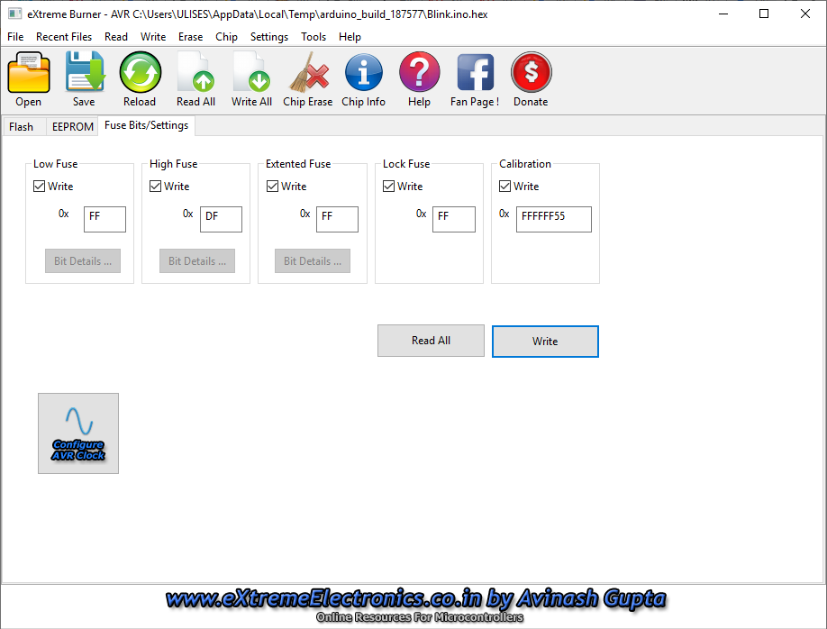
I think that is the most important part, I colocate the fuses, because if the fuses are not the correct it does not work, in the picture you have the secuency:
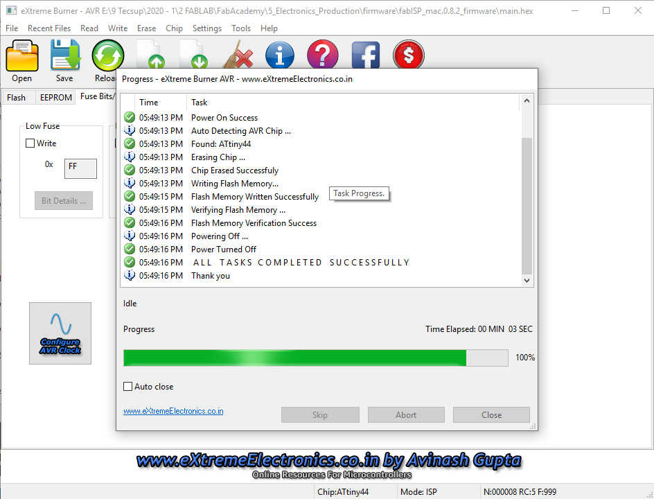
So I program the microcontroller, I click in Write -> All menu, and the programa detects and programs the chip:
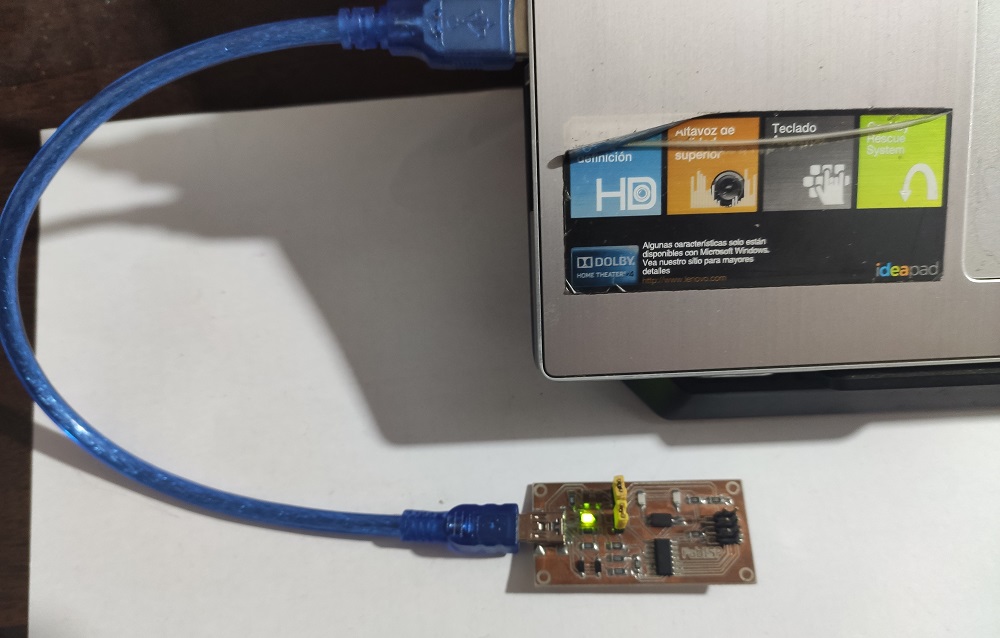
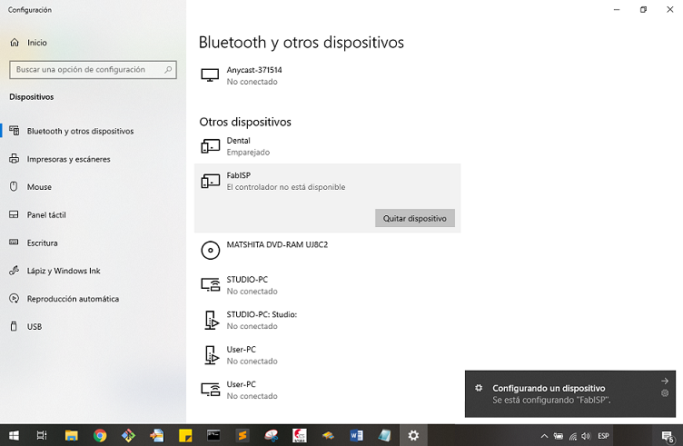
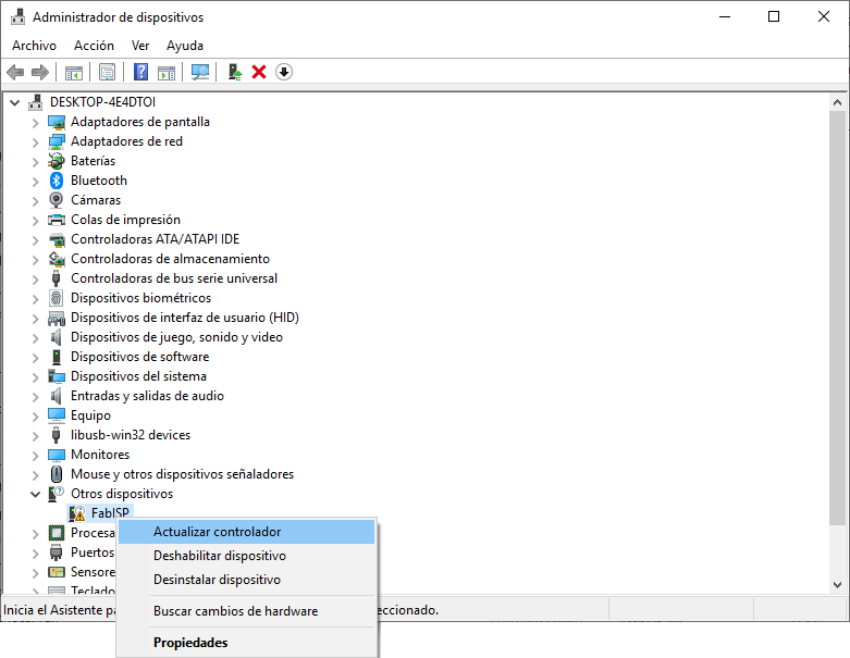
So when I plug the FAPISP the system detect the board:
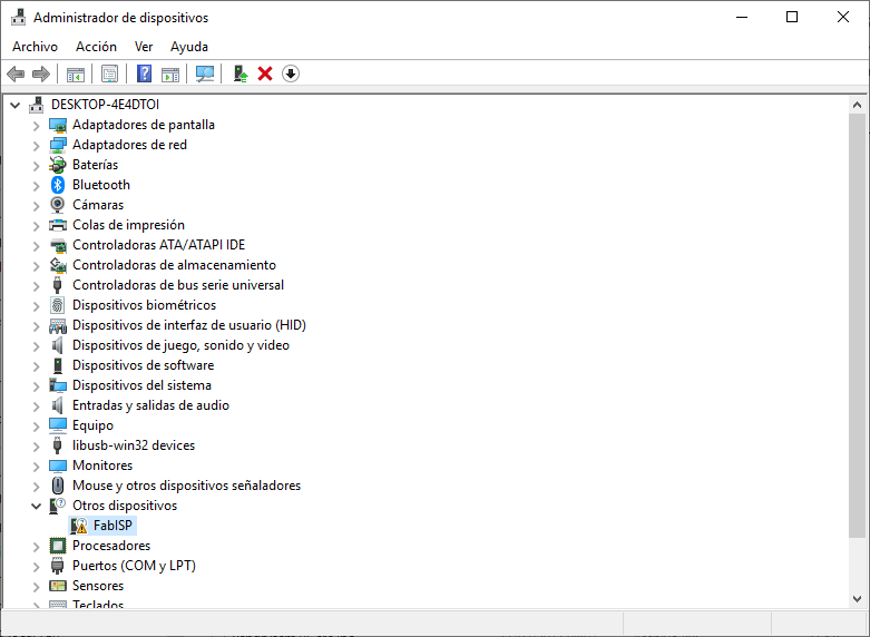
But the system does not have the FABISP driver, and I must install manually
So I must install the official driver
I can download the official driver in https://github.com/adafruit/Adafruit_Windows_Drivers/releases and I can install manually:
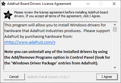
I must choose the USBtinyISP because it is the created board
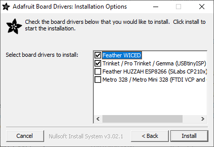
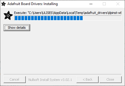
So I click on Install button and the installation started:
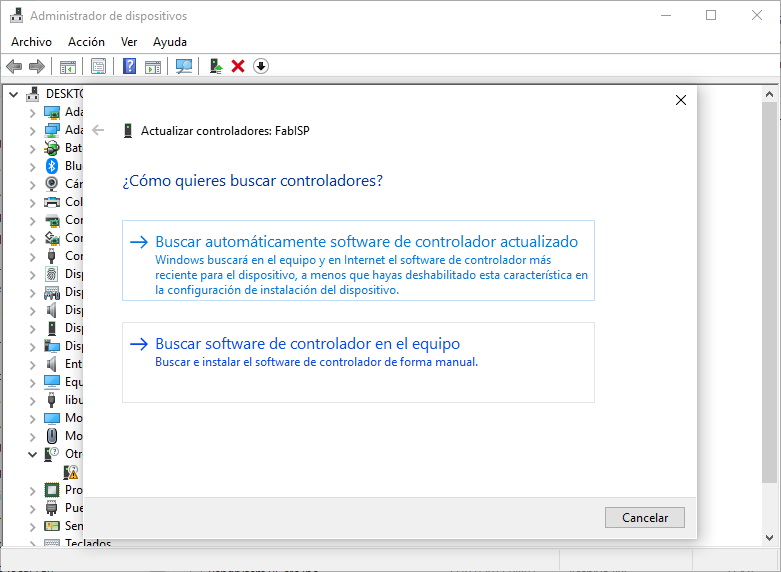
So I must re-install manually the driver:
The system find the driver automatically, I click these:
So the system recognizes the driver and there is not the error again:
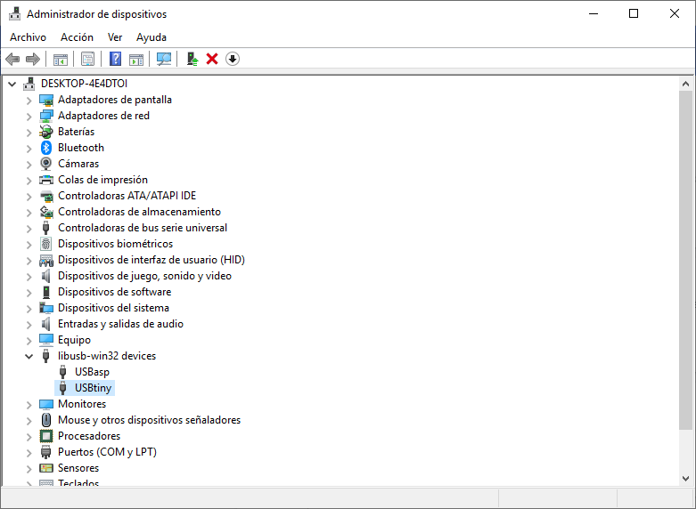
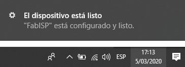
Finally the created board FABISP is configurated and ready to use:
4. Testing the USBtiny
I open the Arduino IDE
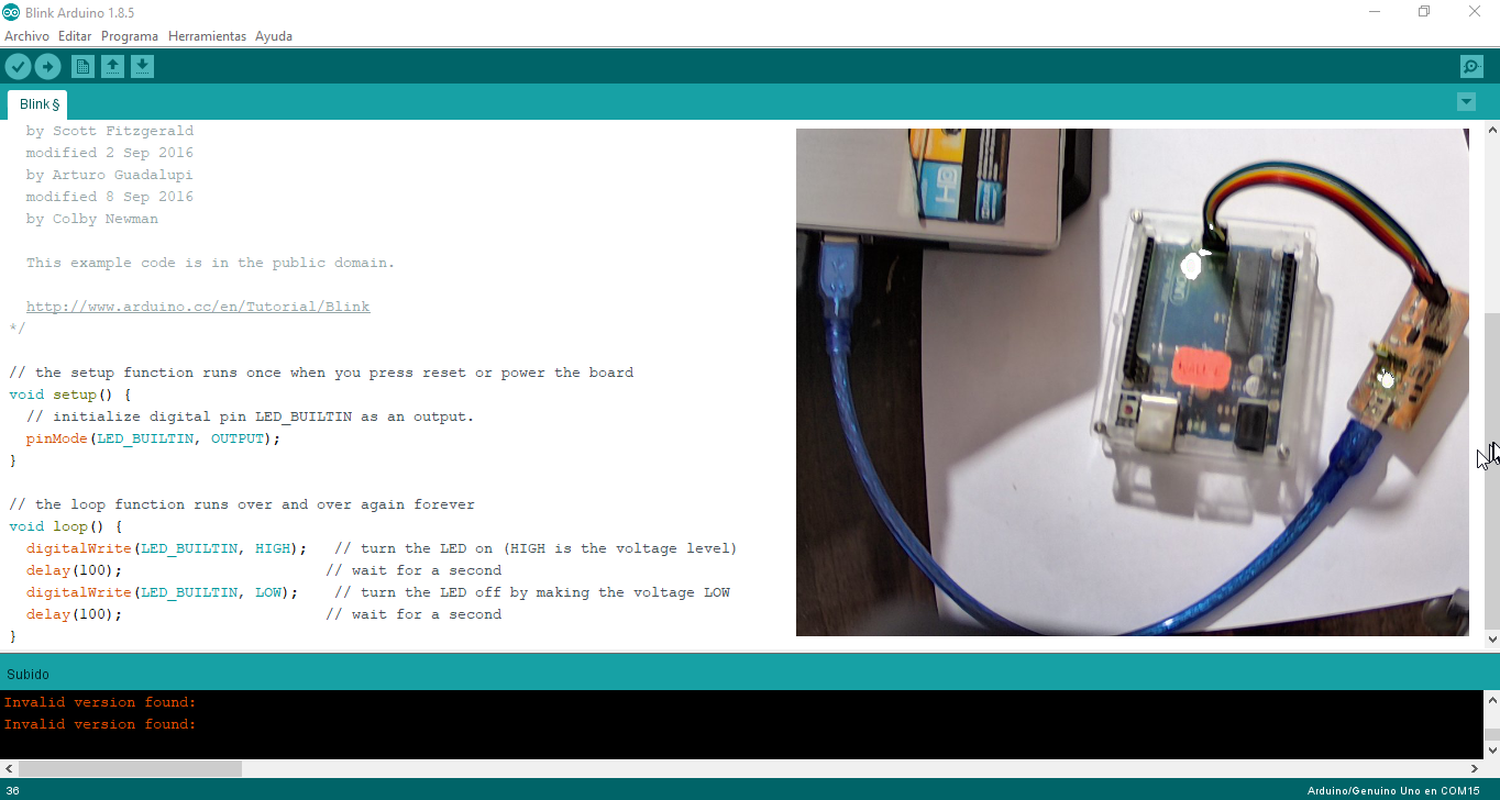
And we can see the demonstration of your work, when the load goes wrong is because the wires do not connect:
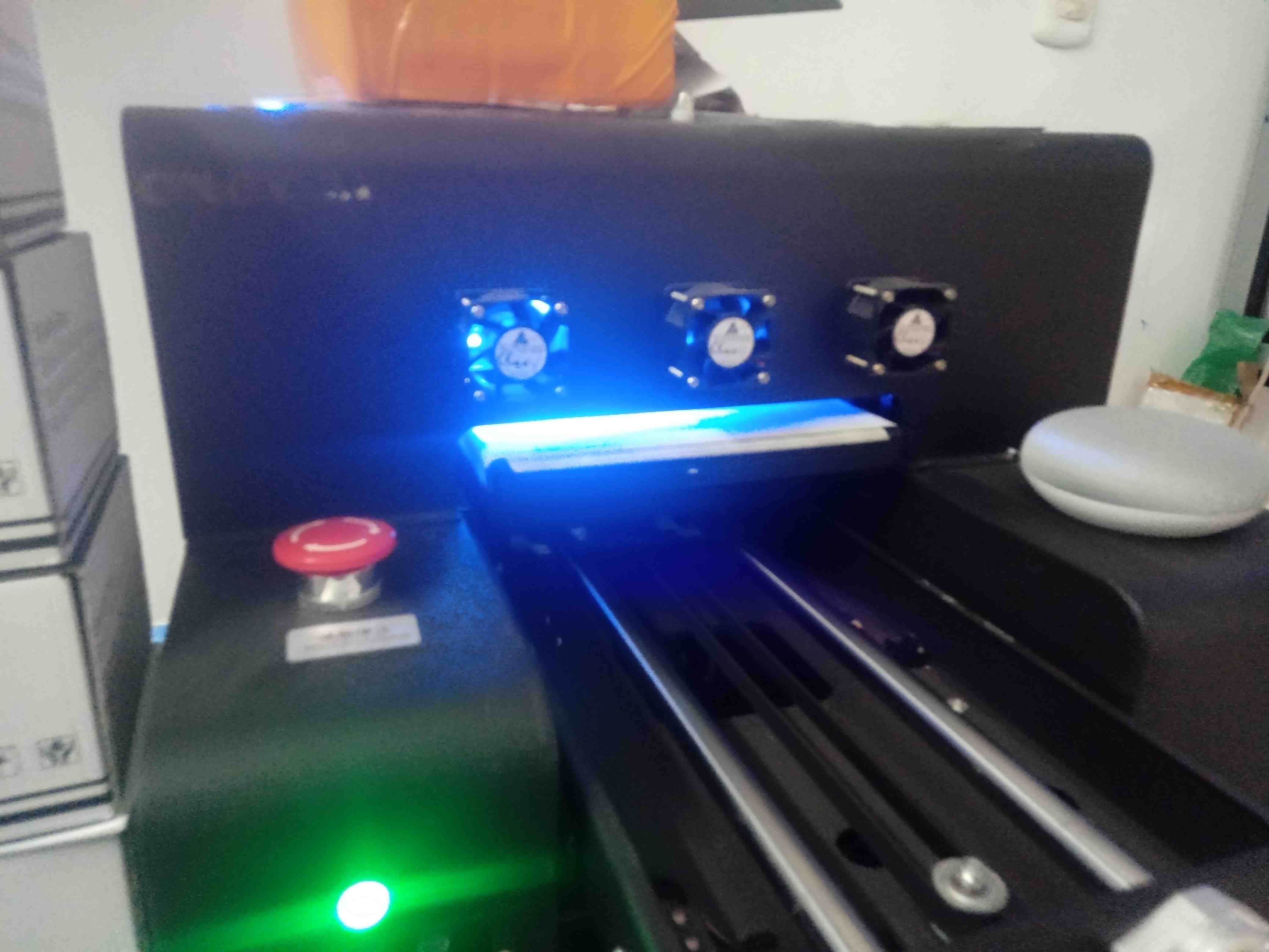
5. Creating soldermask with UV Printer
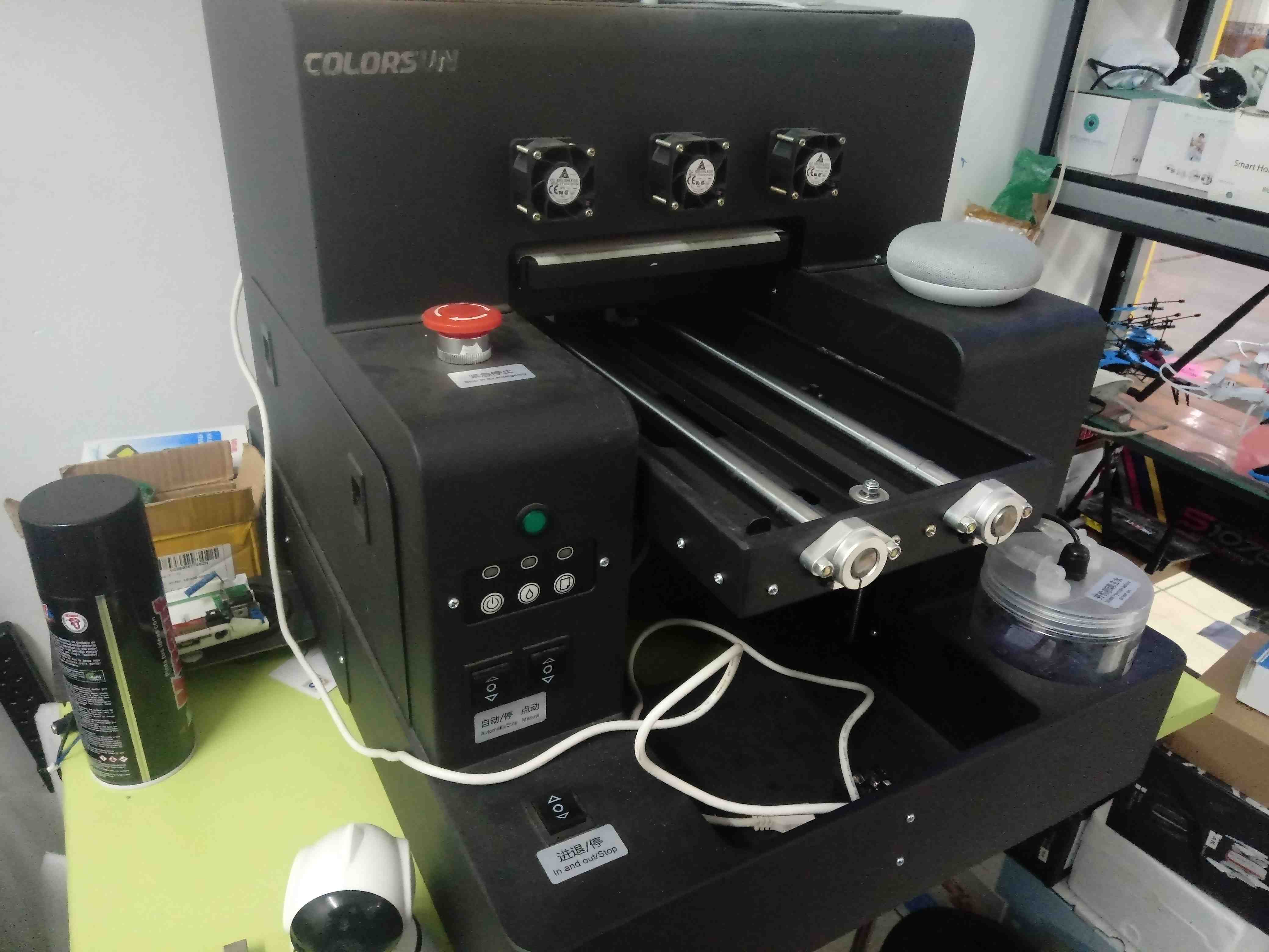
In addition, I did a test with a UV printer to create a PCB with an anti-solder mask, in this case I used a UV printer COLOR IN from a china company, the process did by in a external service, it does no have our FABLAB
We can see printing the anti-solder mask:
The result is here:
I choose the best PCB to solder:
The process was succesful, and we can see the solded PCB board
We can see all solded PCB board:
6. The Successful PCBs
Also the board to work are these:
7. Failed 1: Soldermask with UV Paint
Other way to create a anti-solder mask is applying the UV paint over the inital PCB and curing with a UV light:
Probally I did not work well and the PCB was not cover all, I failed with the soldermask with UV paint.
8. Failed 2: Solder Mask with Stencil and Hot Oven
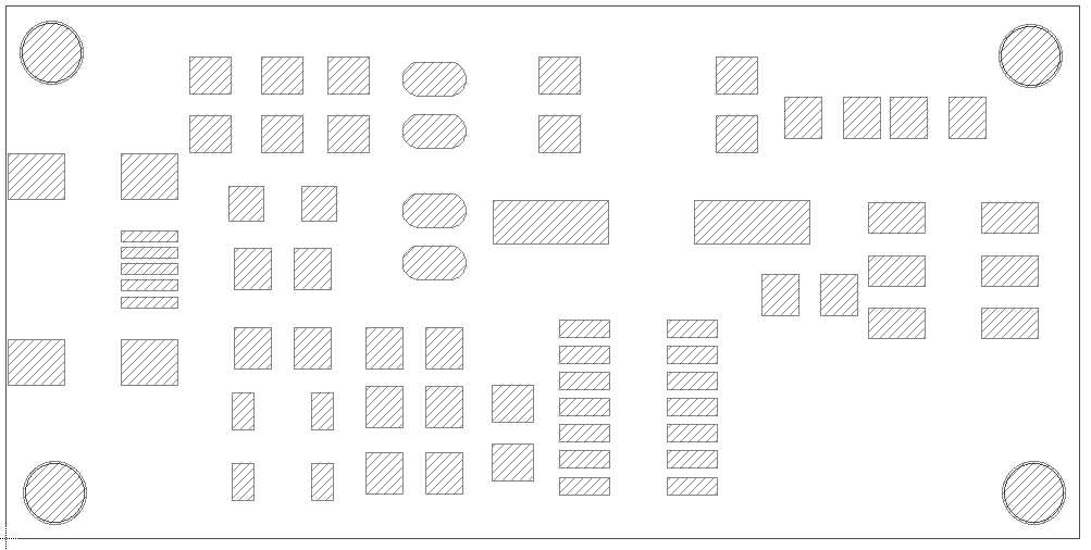
I prepared only the Dimension and tStop layer from Autodesk Eagle:
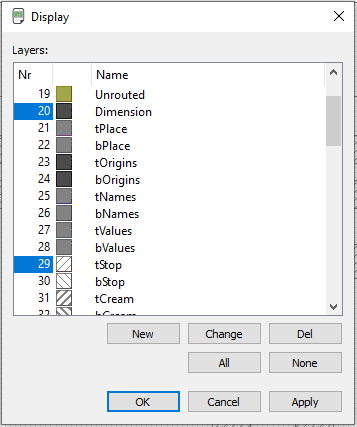
We can see the antisolder mask:
I export the image with DXF file in Autodesk Eagle software:
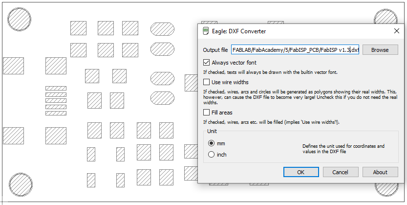
I cut the antisolder mask in CO2 laser cuttin machine in transparent stencil:
I cutted three samples to test:
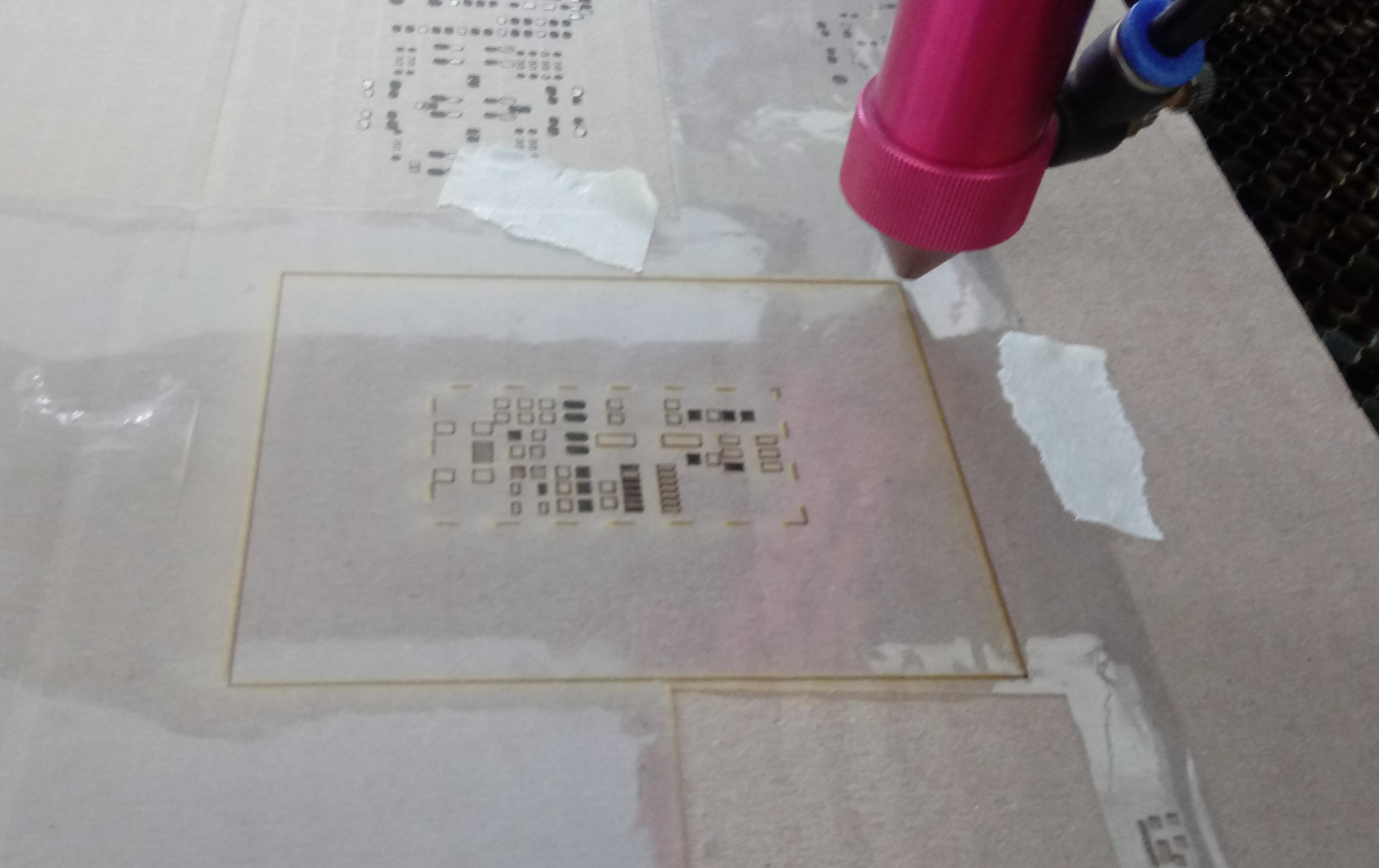
I took the PCB and anti-solder mask to work, with liquid tin covered the holes in the stencil
The liquid tin does not cover correctly the pads; so I failed with the process:
When I try colocate the SMD components the pads are across together, and I failed the process to generate the stencil
Designed Files
| Description | Files |
|---|---|
| Pattern Eagle Schematic | Pattern_Test.sch |
| Pattern Eagle Board | Pattern_Test.brd |
| Pattern Eagle Image | Pattern_Test.png |
| Pattern Router Monofab SRM20 | Pattern_Test.rml |
| FabISP Eagle Schematic | FabISP_v1.0.sch |
| FabISP Eagle Board | FabISP_v1.0.brd |
| FabISP Eagle Image | FabISP_v1.2.png |
| FabISP Router Monofab SRM20 | FabISP_v1.2.rml |
| FabISP Attiny44A Firmware | FabISP_Attiny44A_Firmware.hex |