Module 07 – Electronics Design
Class
In class we flew over all the different types of components we may come across in designing circuits.
That done and over we went on to discuss about designing circuits. At our level, a few rules govern circuit design: Kirchoff's laws and Ohm's law. In layman’s term it gives something like:
- Kirchoff's laws:
- At a node the sum of the current coming in is equal to the sum of currents leaving the node.
- The sum of the voltages in a loop is 0.
- Ohm's law:
- [ I = V / R ]
Circuit CAD
Having assimilated "Electronics 101" in 30 minutes, it was time to address the subject of actually drawing the circuit in order to have it built.
In order to work quickly and properly when designing a circuit, the software should have the following properties:
- Hierarchical drawing
- Parametric
- Integrate a library of footprints for the components we will be using.
Some circuit CAD software integrate the possibility to design the schematic of the circuit and then design the board and the routing directly with the components placed on the schematic.
These software packages include:
The proper workflow in designing a circuit is as follows:
- Design the schematic.
- Layout the component.
- Route the traces (to make the connection between components).
- Model (to validate your design).
- Fabricate.
Modeling
Modeling can be particularly useful to validate your design before spend time milling and stuffing a board that has a design flaw.
Recommended solutions
- SPICE initially a linear equation solver designed at UC Berkeley, it comes with add-ons specific for circuit testing [LTspice ] → a good solution
- Some solutions a bit easier to use and better integrated:
- Grucap
- Qucs
- Oregano
- In the virtual breadboard category:
- 123D circuits
- Virtual Breadboards
- Fritzing
- Multisim
Then there are professional solutions to layout millions of transistor circuits... [Verilog VHDL]
Routing
A lot of art goes in routing. You need to do mental origami to optimize the routing.
In Class Tutorial
There isn't really proper time for tutorial, we each should go about our business, watch the Eagle tutorials, and ask questions as they arise.
The Assignment
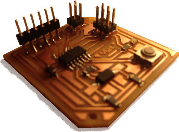
- redraw the echo hello-world board,
- add (at least) a button and LED (with current-limiting resistor),
- check the design rules,
- make it
Redrawing the board (with extra stuff)
The schematic
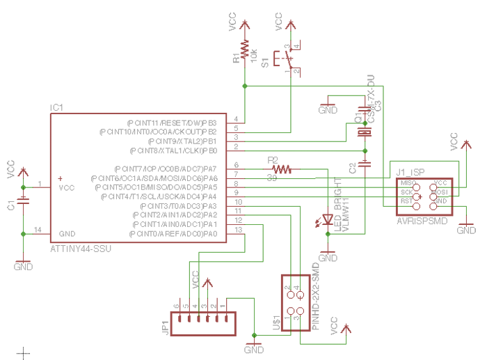
Checking values for
I first drew the board within eagles shopping for parts within the libraries grabbed from the tutorials that I had added to Eagle.
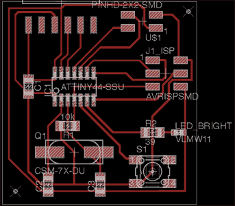
Drawing my paths
Photoshop
I decided to take the PNG file to Photoshop to add the perimeter for cutting with the milling machine… and while I was in Photoshop I touch-up some of the path that I felt hadn’t come out to pretty from Eagle, some path were unnecessarily close to one another, and there were a coup[le of ugly twirls…

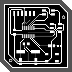
Milling
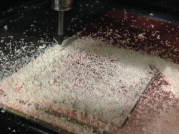
Grzzzzzz…
When I got in the fab module and loaded my PNG fresh out of Photoshop, I got a message about the module not being able to determine the dpi of the file and assuming it was 72dpi. It was just a warning and there was no direct call to action apart from following the normal sequence. So I ignored the message and went on, as the pressure of other students queuing for the machine was felt.
All went fine until I pressed [Mill now]… At this stage the drill started spinning but it took a pretty long time before it started to move about and when it did, it moved from the origin about 1.5 inch in both X and Y and started milling a nice large circle. I kill the job immediately. And realize it had just started milling my design at x7 scale (that I assume by doing a 500/72 ratio).
I assessed the damage by measuring precisely where the unwanted scar had been perpetrated. It looked extremely close to the outer edge of my normally scaled trace, but I made the decision to send the scaled down version. I quickly opened the file in GIMP and . . . . . . . . . . . . . . . . . . . . . . .
The milling went well this time and stood watchful to see if paths cleared the scar. It was extremely close: about half a mil from the edge of the board but still a couple of mm from my first trace.
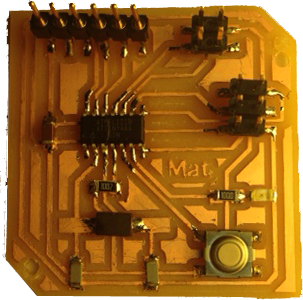
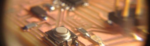
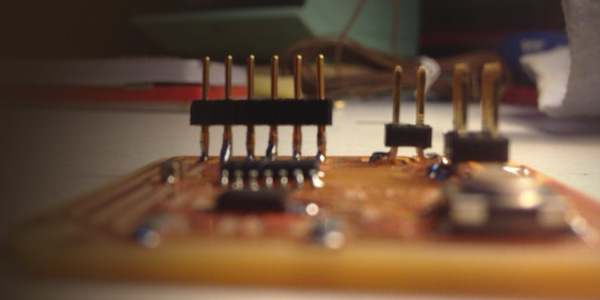
Stuffing
Oh yes I remember the thing that makes you feel nearly blind, I wondered if I shouldn’t have milled my board at a x7 scale after all. Then I might have felt agile stuffing my board…
Time to have another meeting with the real world: what exactly are the components we really have at hand in these plastic drawers
Indeed for sheer lack of time I skipped two steps, one was the modeling, and the other one is the inventory check (that step was not mentioned as it is assumed that in real life you actually design your circuit, and then you go and buy your components ). Where here it’s not quite real life we’re in the comfortable soft-cell of the FabLab Barcelona where all the parts needed are at your disposal (kind of like being in a home where the fridge is always full, and where you let your parents worry about what you’ll eat…)
There is an issue: [better check that there are eggs before you decide on making an omelet].
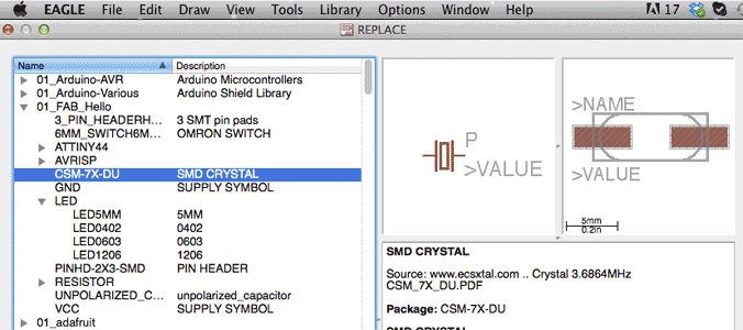
In eagle I picked parts from the shelf (the libraries made available by Neil) without actually checking that I could get my hands on the actual physical components. As it turns out I had to retrofit only two parts:
- The 20Mhz crystal
- A superbright led that I found somewhere and sounded cool.

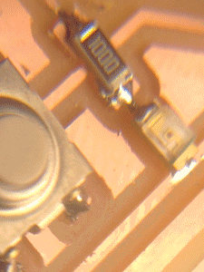
As far the Xtal is concerned I fell in the trap: it said “Xtal1 20Mhz” on the board layout of “Hello_Lab” board, but as everyone knows a crystal has only 2 poles if there are 3 that means it is a resonator (I suppose the resonator is here to teach you to reason: that makes sense). …)
I did figure out that there was something wrong before I started milling, and added two 10pF capacitors between the poles of my crystal an ground. What I did not check is whether the part was available in the lab; and… it was not. What we had was a 12Mhz SMD crystal with a large encasing that matched the footprint of my now milled board, or itsy-bitsy tiny SMD 20Mhz crystal that looked like a cat next to the elephant 12Mhz. I opted for the cat and managed to solder it because the elephant had such humongous footprints.
As for the LED I just picked the standard green led that is in the inventory and there was no size issue as the footprint was equivalent to the one I had chosen.
The trouble was finding the proper resistance value. It is a problem because it is impossible to read any kind of reference on the LED itself. I had to seek help from my guru Luciano; his answer was: "all the components we have here are the ones that are from the FabLab inventory…"
OK, so I:
- Looked up the FabLab inventory:
- Found ref for the green LEDS
- Googled “160-1169-1-ND”.
- Landed on the www.digikey.com page
- Looked up the spec sheet and found the following values:
- DC Forward Current = 30mA
- Forward Voltage (typical) = 2.1V
- I knew from my previous research that the ports output voltage on the AT tiny 44 was 5.0V.
With these values I calculated a value of 87 Ohms (instead of the 37 Ohms I had found for my superbright LED). I used a 100 Ohm resistor.
That's all Folks.