_______________ ELECTRONICS DESIGN _______________
GOALS:
- GROUP ASSIGNMENT:
Use the test equipment in your lab to observe the operation of a microcontroller circuit board (in minimum, check operating voltage on the board with multimeter or voltmeter and use oscilloscope to check noise of operating voltage and interpret a data signal)
- INDIVIDUAL ASSIGNMENT:
Redraw one of the echo hello-world boards or something equivalent, add (at least) a button and LED (with current-limiting resistor) or equivalent input and output, check the design rules, make it, test it.
| DESIGN |
_________________________ EAGLE _________________________
For this week assignment, I choose to redesign the ATtiny45 by adding a button and a LED.
I used Eagle as my PCB Design Software.
EAGLE is an electronic design automation (EDA) software
from AUTODESK and its free download is only available with a Fusion 360 subscription.
Adding a library to EAGLE
The first thing I did was adding the "fab.library", optimized for EAGLE, into my Eagle libraries.
To do this, I followed a tutorial on adding a library to Eagle-Cad. From Eagle control panel I clicked on
Option -> Directories . Then on Browse and search the path were you saved the "fab.library" after having dowloaded it.
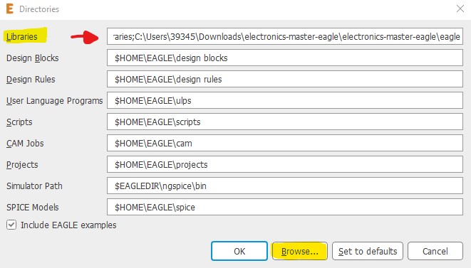
After that, the
fAB.lbr shoud appear in you library. Remember to activate the new library by right clicking on it and pinned the voice USE.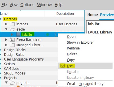
Creating a new project
For creating a new project, from the control panel, I right clicked on
Project , I selected New Project ,
then with a right click on the new project I went to New -> Schematic .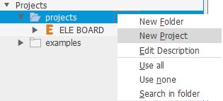
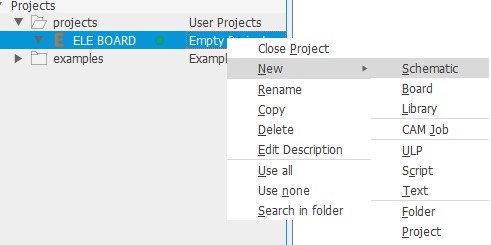
SCHEMATIC
After opening the schematic, I started adding the needed components with add part.
I also wrote their name and value with the tools value, name .
I connected the schematic diagrams with net .
Components:
- Microcontroller: UC_ATTINY45SI
- ISP: CONN_03X2_AVRISP - 2X03SMD
- Connector: pinhead -> PINHD-1X6
- Umpolarized Capacitor (1uF): CAP_UMPOLARIZED C1206FAB
- Resistor 1 (10k), R2 (1k), R3 (150 ohm)
- Led
- Switch tactile 6mm

After connecting all the components, my final schematic looked like this:
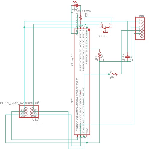
At that point I could switch from schematic to board, by clicking on the icon on the upper toolbar, and start the routing process.

ROUTING
Before starting the routing process, I modified the design rules with the best fitting parameters for my LAB's milling machine, the same ones that our class found during the group assignment for the Electronics production week.
To change the design rules settings I went to Design Rules icon in the right-side toolbar.
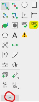
I changed all the
clearanceparameters to 16 mil.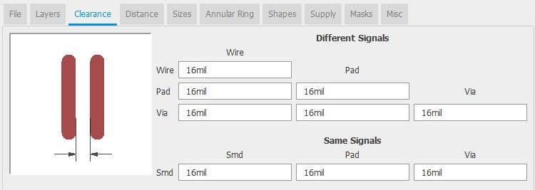
I changed also the
distance copper/dimension and digger/hole to 16 mil.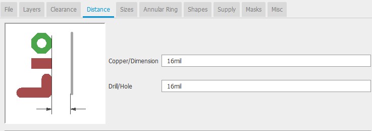
And I changed the minimum width
sizes to 12 mil.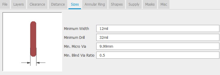
For the routing process I clicked on the
route icon  . Be sure that the connection between
the routes is correctly done (a sort of yellow X sign, like the one in the image below, should appear everytime the routing is correctly done).
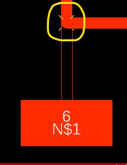
Once I had routed all the components, go to
Design Rules -> File -> check to analyze hidden mistakes.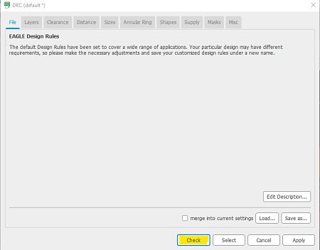
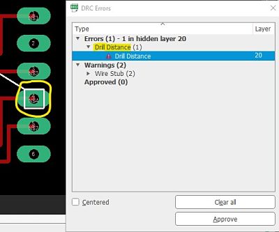
Eventual errors will appear in a "DRC errors-Type" window, and EAGLE will highlight the area/section of the problem, as the image below shows:
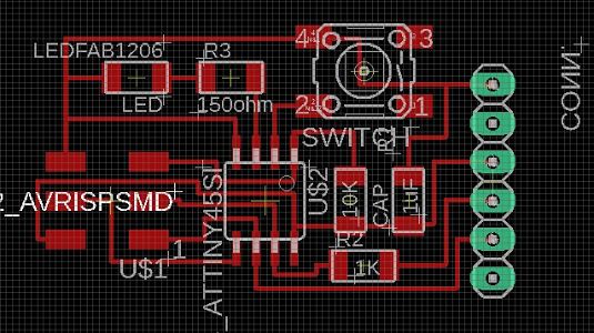
After having correct all the mistakes, my final, routed PCB looked like this:
Now I needed to export the image without names and values all over the place, so I clicked on the
Layer Settings icon  and hide all the layers except for the
 top and pads ones.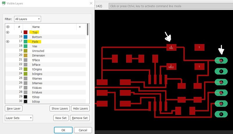
But as you can see, there are still values on the switch and pinhead components, so to hide also them, from the upper toolbar, I clicked on
Option -> Set -> Misc . And I unmpinned the options Display pad names, Display signal names on pads, Display signal names on traces, and Display via lengths.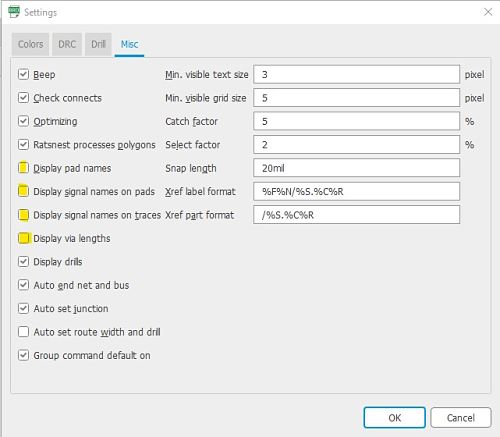
After that, this was the final design of the PCB, ready to be exported:
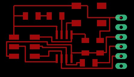
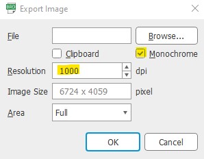
When you export the file, remember to export it as Png image, pin the monochrome option (because the milling machine can read just black and white features), and set a 1000 dpi resolution at least.
________________________ MODS _________________________
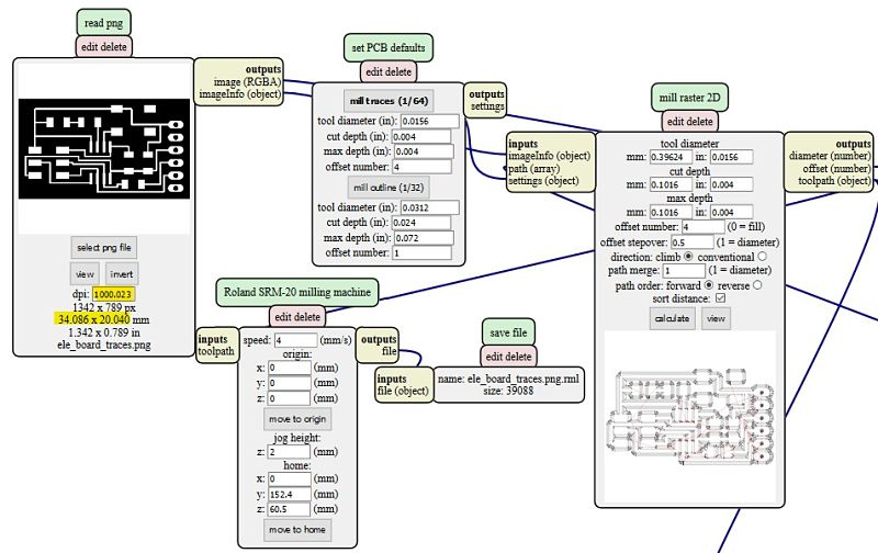
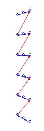
I imported the .png images on mods, to convert them in the milling machine language
.rml .I followed the path for the Roland SRM-20 Milling Machine:
Program -> Open server programs -> Roland SRM-20 -> PCB png.I imported the traces file and checked that that the resolution was 1000 dpi nad i also checked the size (this is important for the outlines and pinheads file, because all the files will have to have the same size).
In the set the PCB defaults I clicked on
mill traces 1/64 .In the Roland SRM-20 milling machine , I setted the xyz to 0.
Then, i clicked on
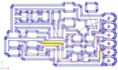
calculate, checked from the view that the cutting was clean and that the traces were correctly separated
from each other.As my Instructor make me notice, and you can even see it from the image below, some traces were too closed to each other. Next time I should carefully check the distance between the traces and trying to add more space between them.
I did the same for the outline file, just changing the set the PCB defaults to
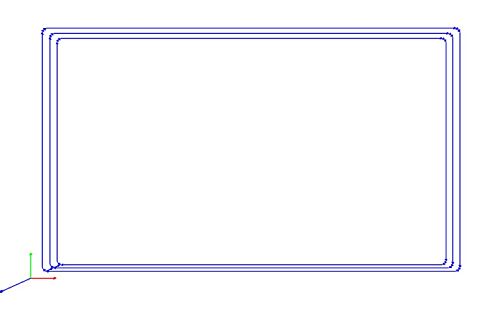
mill outline 1/32.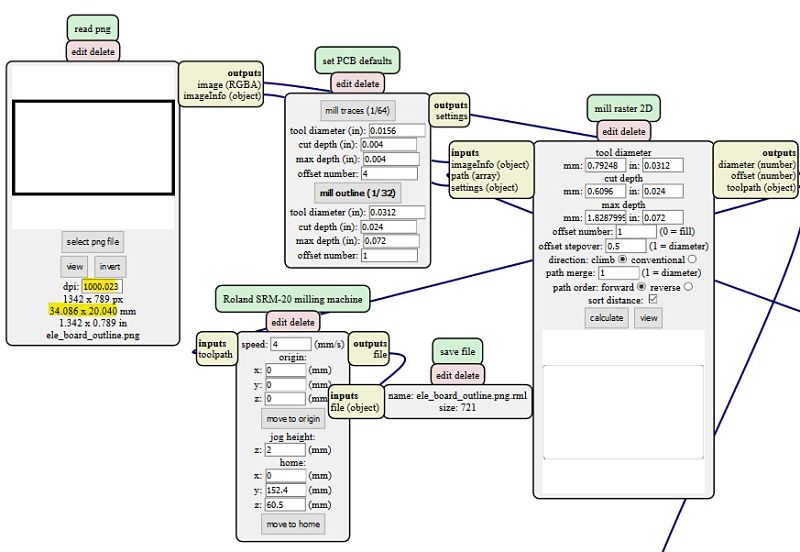
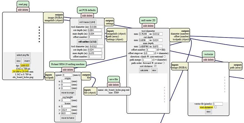
I also followed the same process (selecting mill outline 1/32) for the pinheads file, but when I clicked on calculate it didn't calculate the parameters at all, and the section remained empty.
After wondering what to do, the Instructor tried changing some module's parameters here and there, and we eventually find out the problem. It was correlated with the feature
sort distance in the vectorize module. I unpinned that feature and this time, after clicking on calculate, the vectorized image appeared.
| MILLING |
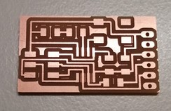
Once I had a .rpl file for the traces, the outline and the pinehead holes, I was ready to mill. I firstly milled the traces, and I had to do it twice because some traces weren't separeted well because the board section that I had choose was not completly levelled. Then, I decided to mill the pinehads holes, and milled the outline as the last.
| SOLDERING |
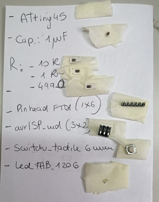
B.O.M:
- Microcontroller: UC_ATTINY45SI
- avrISP (03X2)
- Pinhead connector-> PINHD-1X6
- Capacitor (1uF)
- Resistors:
___R1 (10k)
___R2 (1k),
___R3 led resistor (150 ohm): I followed a site for calculating the led resistor value.
I calculated it by using the Source voltage: 5V, the Diode forward voltage (2.0 V for orange led), and the diode forward current (20 mA).
- Orange Led (2.0 V): Remember that LED is a diode. In Diods the current flows in the direction of the arrow (cathode), which in LED component is segnalated by a green line. The LED cathod must be connected to GND ( you want all the GND in your PCB to be connected) in order to dissipate the LED current.
- Switch tactile 6mm
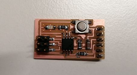
After having listed all the needed components, I started soldering and it was way much easier than the first time, thanks to an improved technique and lot of patience the result made me so proud.
| PROGRAMMING |
The last step was testing my PCB by successfully programming it. So, I used the programmer I created during the Electronics production week.
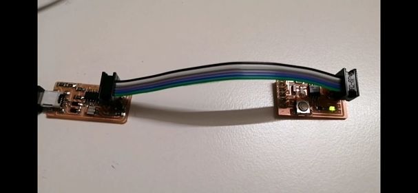
I connected my programmer to my new PCB through a ribbon cable.
Then, i connected the programmer to the computer through an USB cable.
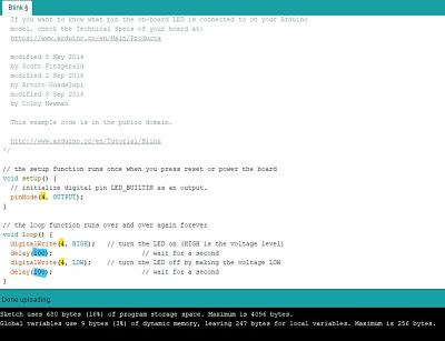
I tried programming the programee it with Arduino and it successfully worked with the firt attempt, the LED blinked!
