ELECTRONICS PRODUCTION
Assignment Overview
Group Assignment
- Characterize the design rules for your in-house PCB production process
- Submit a PCB design to a board house
Individual Assignment
- Make and test an embedded microcontroller system that you designed
- Extra credit: make it with another process
Group Assignment
This week's group assignment focused on characterizing the design rules for our in-house PCB milling process. By systematically testing different trace widths, clearances, and via sizes on the Roland Modela MDX-20, we established reliable minimum values that guide all future PCB designs produced at our lab. Understanding these limits before committing to a design prevents frustrating rework and wasted material.
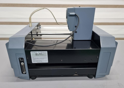
PCB Milling Machine — Roland Modela MDX-20
The Roland Modela MDX-20 is a compact desktop CNC milling machine widely used across Fab Labs for PCB fabrication. Rather than etching copper with chemicals, it mechanically removes unwanted copper from FR1 copper-clad boards using precision carbide end mills. This dry, subtractive process produces single- or double-sided boards entirely in-house, with no chemical handling required.
Key specifications of the MDX-20 relevant to PCB work:
- Working area: 203 × 152 × 60.5 mm (X × Y × Z)
- Positional accuracy: ±0.01 mm — adequate for SMD pads down to 0402
- Spindle speed: 6,500 RPM (fixed)
- Typical end mills: 1/64" (0.4 mm) for trace isolation; 1/32" (0.8 mm) for board outline
- Control interface: VPanel (Windows) or Mods CE browser-based CAM
The full group documentation is available here.
Individual Assignment — Making the PCB
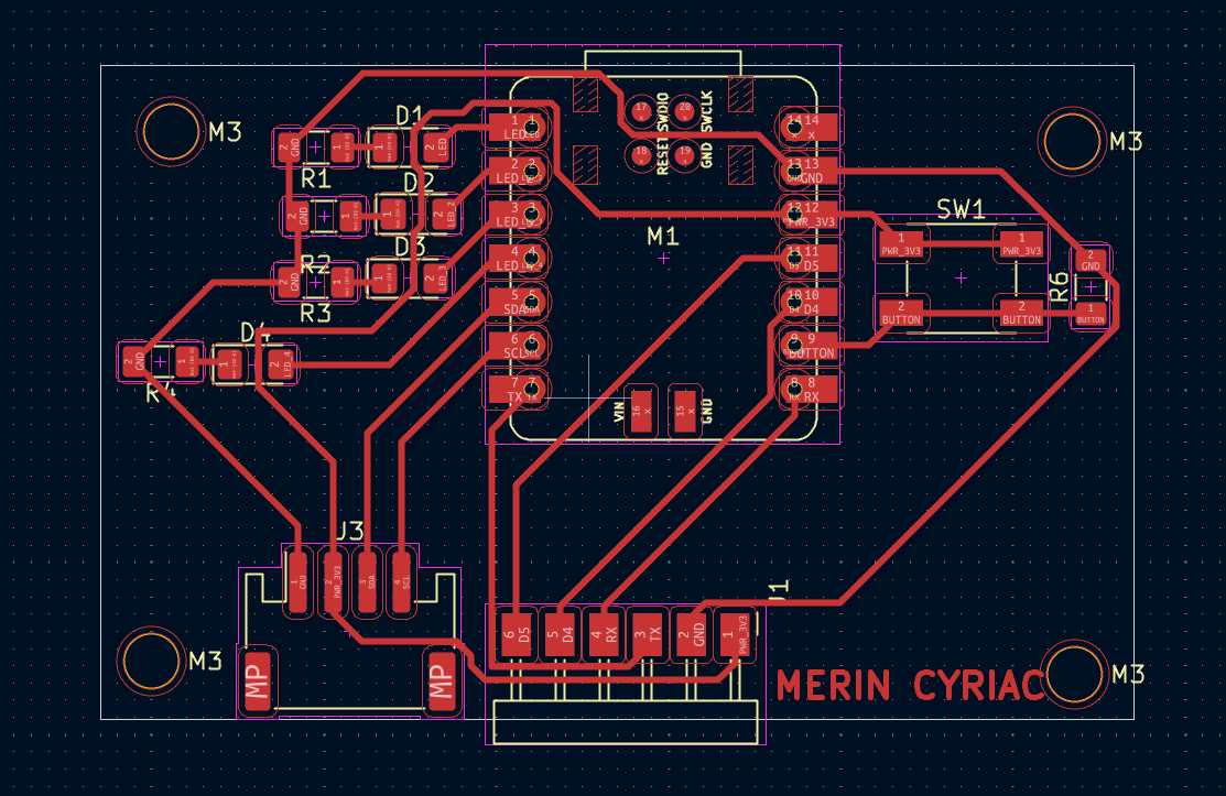
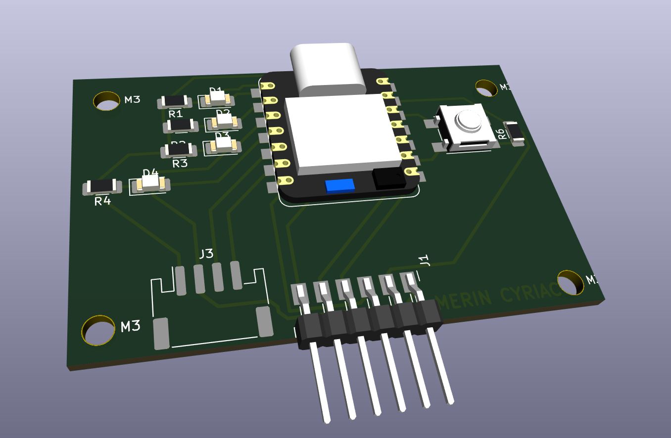
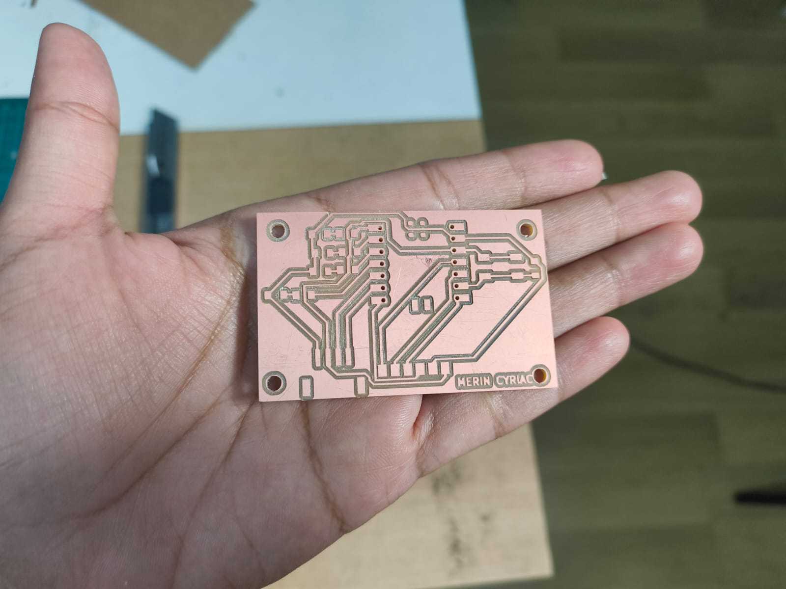
For the individual assignment, I fabricated the PCB I had designed during Electronics Design week (Week 06) — a custom board built around the Seeed Studio XIAO RP2040 microcontroller. The board was milled, stuffed with SMD components, soldered, and tested entirely within the Fab Lab.
The design features the XIAO RP2040 as the central processing unit, a tactile push button for user input, an SMD LED with a current-limiting resistor as a visual indicator, and pin headers for I/O breakout.
Step 1
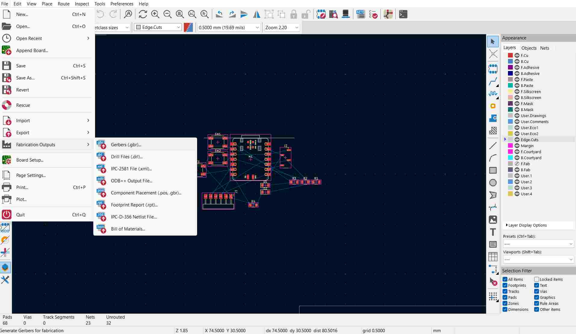
Exporting Files
Before loading anything into the CAM tool (Mods CE), the PCB layout must be exported from KiCad and converted into a format the milling machine understands. This is a two-stage process: first exporting Gerber files from KiCad, then converting the relevant copper layer to a high-resolution black-and-white PNG that Mods CE reads as its input image.
Exporting Gerber Files from KiCad
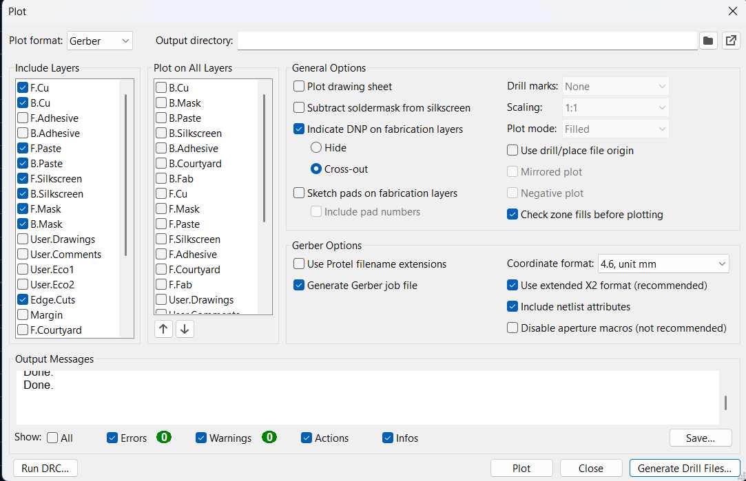
In KiCad's PCB editor, I navigated to File → Fabrication Outputs → Gerbers to open the Plot dialog. The following layers were selected for export:
- F.Cu — front copper layer (traces and pads)
- F.Mask — solder mask openings
- F.Silkscreen — component labels and reference designators
- Edge.Cuts — board outline, used for the cutout toolpath
What Are Gerber Files?
Gerber files are the universal standard for communicating PCB design data to fabrication equipment.
They describe each physical layer of a PCB as a separate file containing vector graphics instructions: where copper should exist, where solder mask openings should be, where silkscreen text should print, and where the board edge should be cut.
Each layer of your board maps to a dedicated Gerber file:
- F.Cu / B.Cu — front and back copper layers (traces, pads, fills)
- F.Mask / B.Mask — solder mask openings over exposed pads
- F.Silkscreen / B.Silkscreen — component reference designators and markings
- Edge.Cuts — the board outline used for routing or milling the perimeter
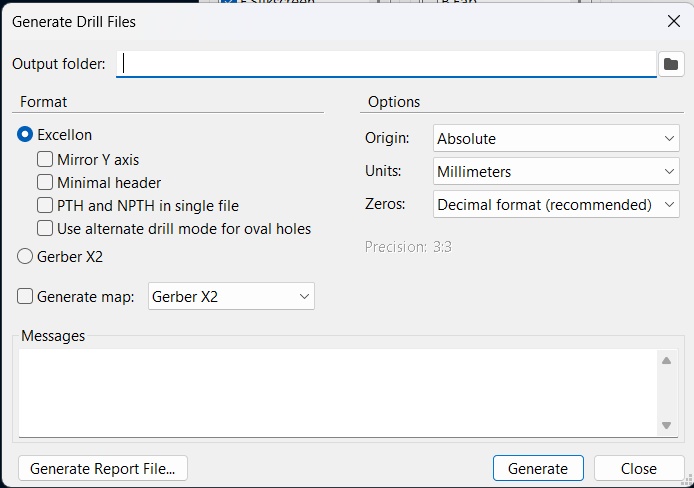
- Excellon drill file (.drl) — hole positions and diameters (technically a separate format, always included alongside Gerbers)
Together, this set of files forms a complete description of the board.
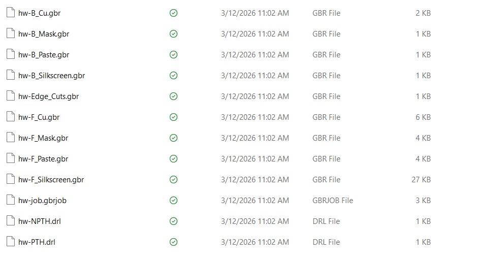
In the context of this week's workflow, Gerber files served two distinct roles. For the board house submission (JLCPCB), the full Gerber package was zipped and uploaded directly — the board house's automated system reads each layer and produces the finished PCB. For in-house Roland MDX milling, Gerbers cannot be used directly because Mods CE requires a raster image input; the Gerber files were therefore converted to high-resolution PNGs using the Gerber2PNG tool, which renders each layer as a precise black-and-white bitmap that Mods CE can process into machine toolpaths.
Converting Gerbers to PNG with Gerber2PNG
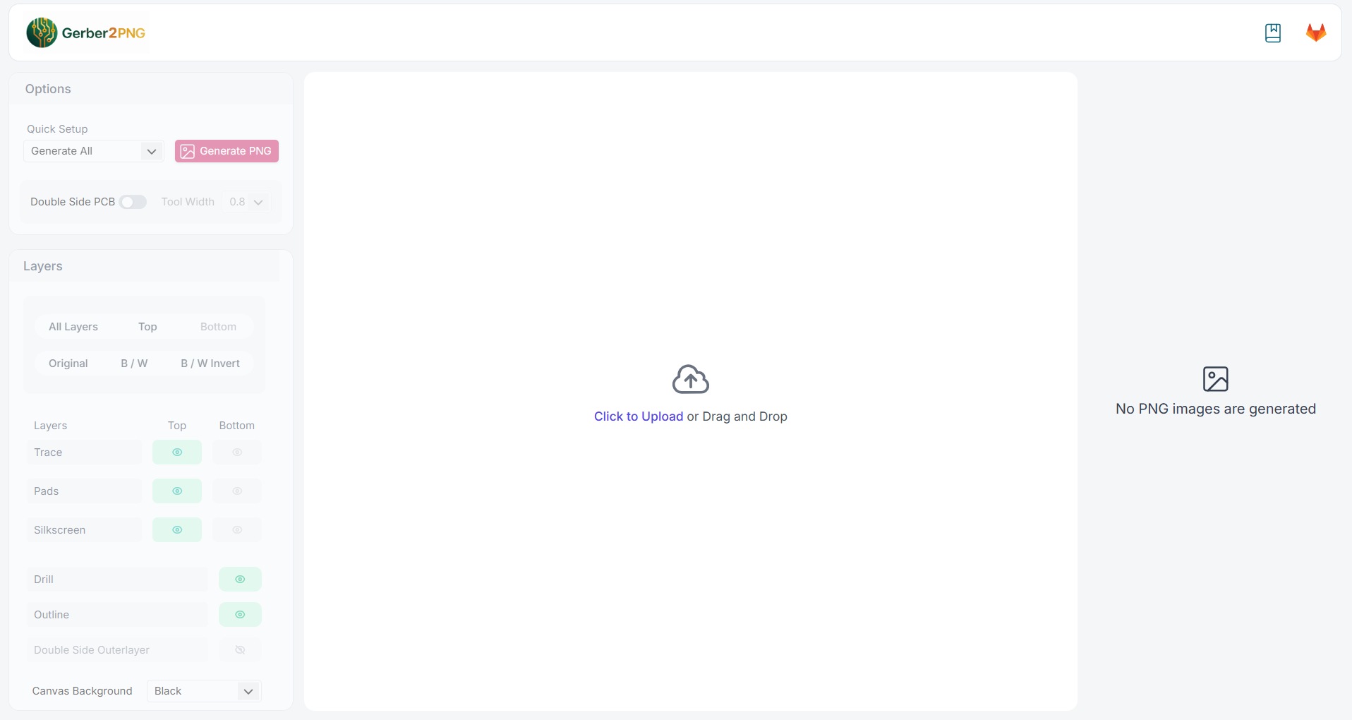
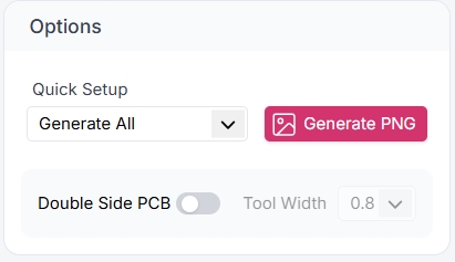
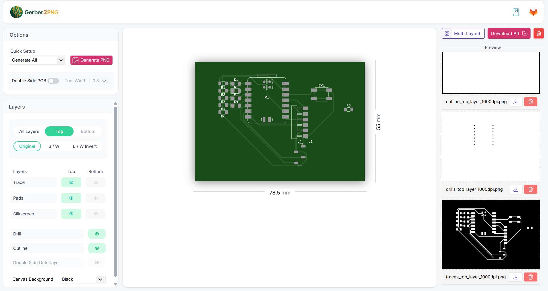
Mods CE does not read Gerber files directly, it needs a raster image where copper regions are black and gaps are white. To produce this, our lab uses the Gerber2PNG web tool hosted at gerber2png.fablabkerala.in, developed by Fab Lab Kerala.
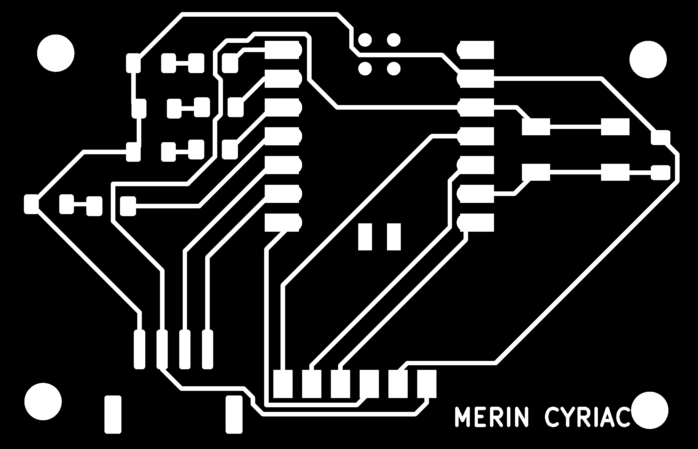
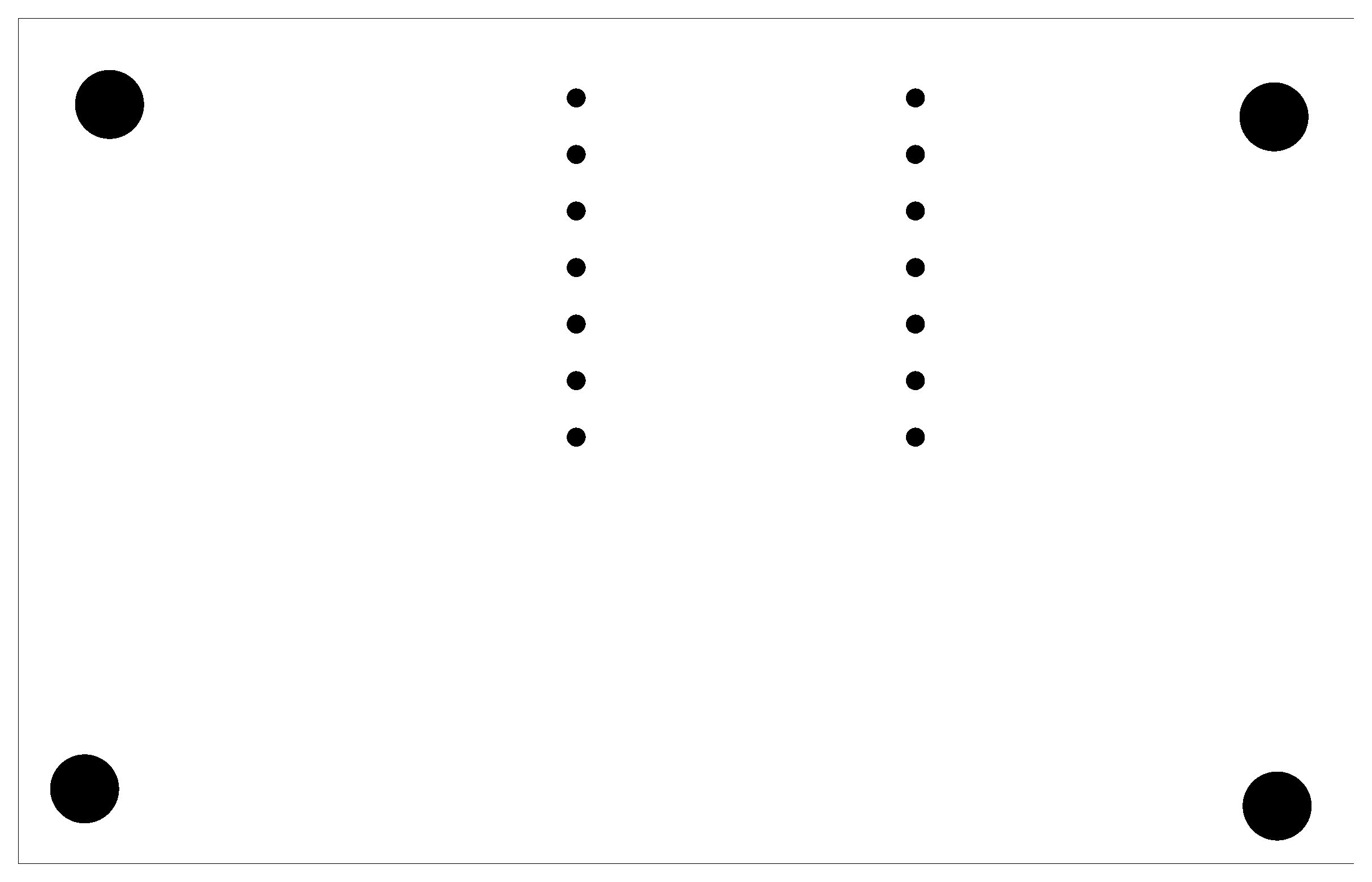
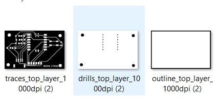
I uploaded all exported Gerber files to the tool, selected Generate All to produce PNG layers at 1000 DPI, and downloaded the resulting images, one for the copper traces, one for the edge cuts, and one for the drill positions.

Gerber2PNG KiCad Plugin
Fab Lab Kerala also maintains a dedicated KiCad plugin version of the Gerber2PNG tool that integrates directly into the KiCad toolbar. Rather than switching to a browser-based workflow, this plugin lets you convert Gerbers to PNG with a single click from within KiCad, streamlining the process considerably.
It can be installed through KiCad's built-in Plugin and Content Manager or manually from the GitHub repository. Once installed, a toolbar button appears in the PCB editor. Clicking it generates the trace, edge-cuts, and drill PNGs at the correct resolution for milling, without leaving the application.
The plugin is open source: Gerber2PNG
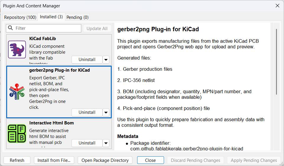
Installing the Gerber2PNG KiCad Plugin
The plugin is distributed as a ZIP archive from its GitHub repository. Installation is handled entirely through KiCad's built-in Plugin and Content Manager, requiring no manual file copying or command-line steps. The four-step process below covers downloading the archive, opening the manager, installing from file, and confirming the installation.
Step 1 — Navigate to the GitHub repositoryOpen the plugin's GitHub repository at the link provided above. On the repository's main page, click the green Code button and select Download ZIP to download the full plugin archive to your machine. Save it to a memorable location — you will need to browse to this file in the next step.
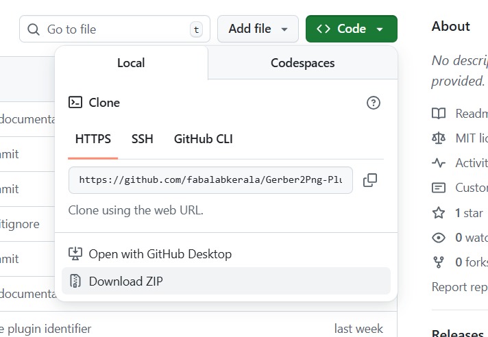
Confirm the ZIP file has been saved to your local machine. The archive contains the plugin's Python source files, metadata, and any required assets.
Step 2 — Open the Plugin and Content ManagerIn KiCad's main project window (or from within the PCB editor), navigate to Tools → Plugin and Content Manager. This opens the manager, which lists all installed plugins alongside available packages from the official KiCad repository.
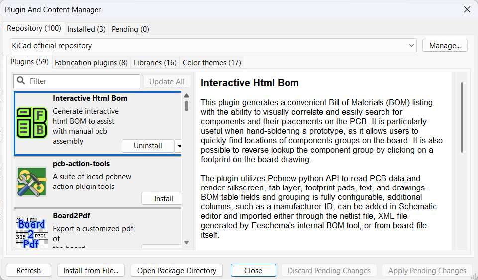
For a local installation from file, the standard repository listing is not used — instead the Install from File… button at the bottom of the window is used to bypass the online catalogue entirely.
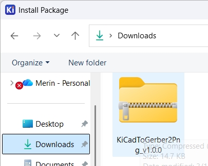
Step 3 — Install from file and select the ZIPClick Install from File… to open a file browser dialog. Navigate to the location where the plugin ZIP was saved and select it, then click Open. KiCad will extract the archive, register the plugin, and prompt you to apply pending changes. Click Apply Pending Changes to complete the installation. A new toolbar button for Gerber2PNG will appear in the PCB editor on the next launch.
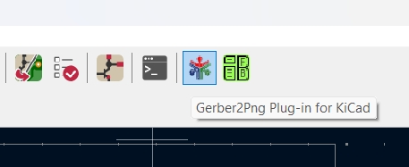
Once the PCB design is complete, clicking the Gerber2PNG toolbar button launches the tool directly in the browser with the current board's Gerber files pre-loaded — no manual export or file browsing required. A single click on Generate All produces the trace, edge-cuts, and drill PNGs at the correct resolution, ready to be fed straight into Mods CE for toolpath generation.
Step 2
Generating Toolpaths with Mods CE
Mods CE (Community Edition) is a browser-based, modular CAM tool developed and maintained by the Fab Academy community. It runs entirely in the browser with no installation required and converts the PCB PNG images into machine-ready .rml toolpath files for the Roland MDX/SRM-series mills. You can access it at modsproject.org.
You can take the PNG imgaes generated form the Gerber2PNG and load it into the Mods CE and generate the toolpath for milling.
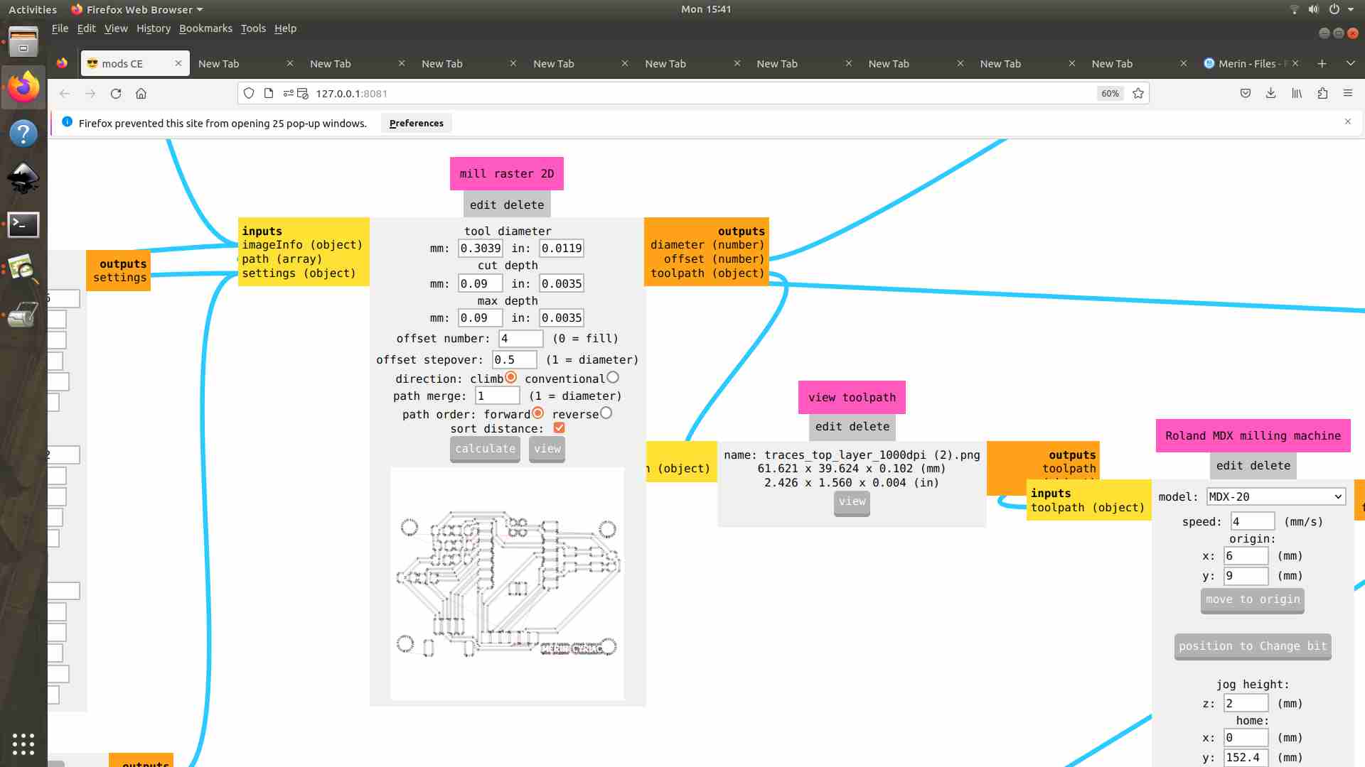
Unlike traditional desktop CAM software, Mods CE uses a visual, node-based pipeline, you connect processing modules together to chain operations from image input through to machine output. The community provides pre-built programs for common machines, so most users only need to load a program and adjust a few parameters.
I opened Mods CE in the browser and right-clicked the canvas to bring up the program menu, then navigated to:
- Programs → Open Server Program → Roland MDX mill → PCB PNG
This loads a pre-built node network configured specifically for the Roland MDX-20, including modules for reading a PNG, computing isolation offsets, generating the mill path, and outputting Roland RML commands.
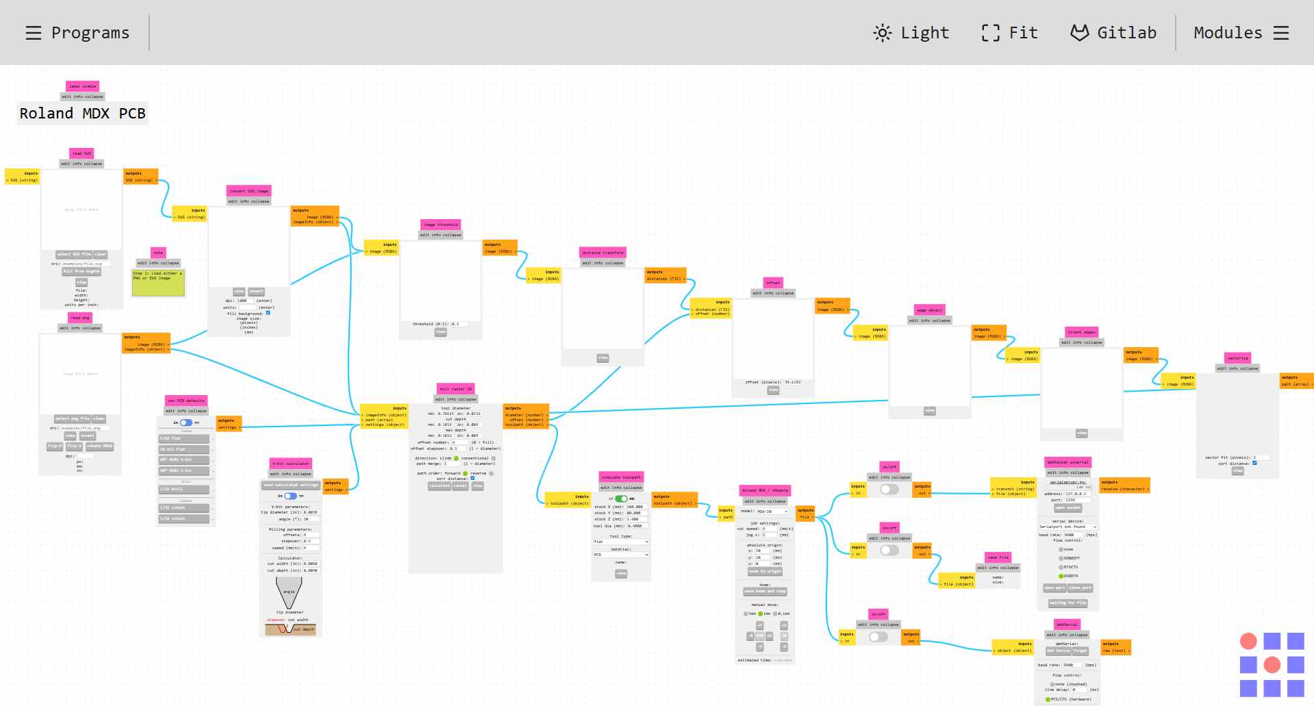
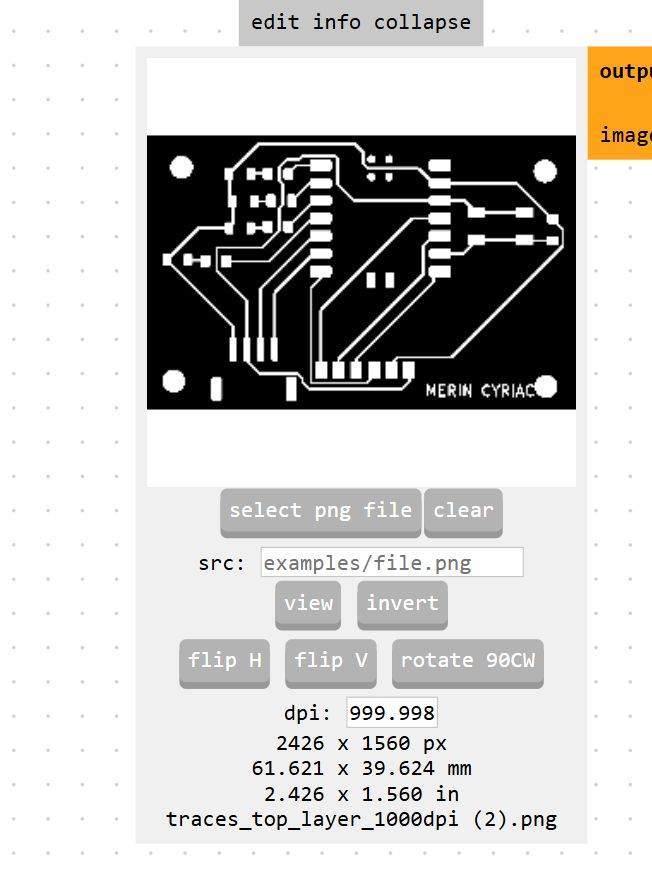
I clicked the select png image module and loaded the copper trace PNG exported earlier.
The image must be strictly black and white: copper areas appear black, and the areas to be milled away are white. Mods CE reads the image dimensions and embedded DPI metadata to correctly scale all toolpath coordinates into real-world millimetres.
The milling process follows a fixed sequence: traces are engraved first, then component holes are drilled, and finally the outline is cut to release the board. This inside-out order ensures the copper layer remains firmly held in place throughout each operation.
So the traces are loaded first.
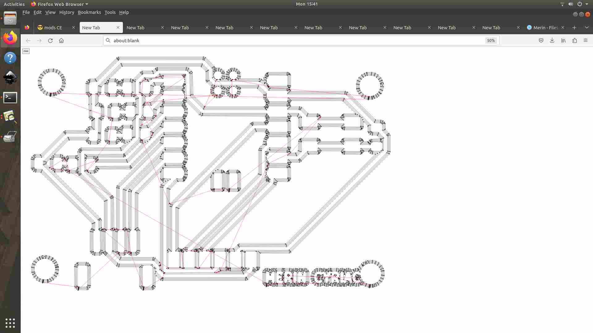
Before sending any commands to the machine, Mods CE renders a live preview of the computed toolpath in the view module.
I carefully inspected the preview to confirm:
- All traces were correctly isolated with adequate clearance on both sides
- No toolpath line crossed over an existing trace (which would cause an electrical short)
- The board outline was absent — that runs as a completely separate operation with a different bit
- Pad areas for SMD components were preserved and not accidentally milled
Changing the Bit
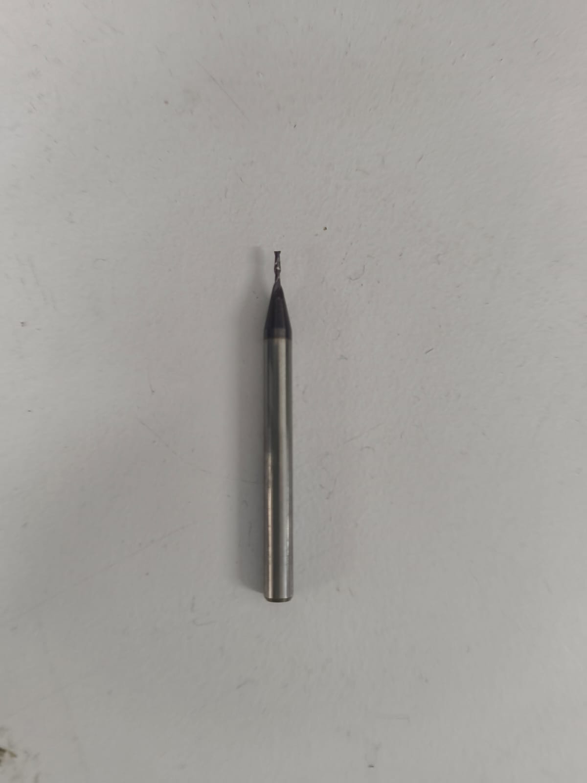
PCB milling on the Roland MDX requires two separate bits, each used for a different operation. The V-bit (0.2 mm tip) is used for engraving the copper traces, while the 1/32" (0.8 mm) end mill handles drilling and the board outline cutout.
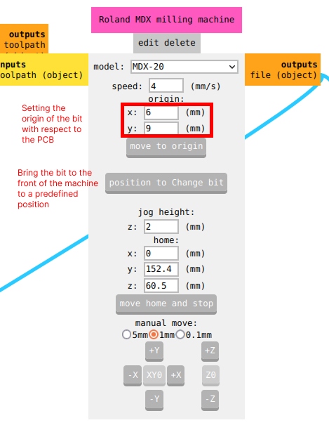
Setting Parameters and Zeroing Z
With the V-bit in, I used the V-bit calculator to get the right cut parameters. Depth came out to 0.09 mm, offset set to 4. Then I zeroed Z manually — lowering the bit slowly until it just touched the copper surface, then tightening it in place. Getting this right matters a lot. Too shallow and you leave thin copper bridges between traces. Too deep and you're cutting into the FR1 substrate and the bit wears out fast.
Sending the File
Back in Mods, I opened the socket and hit Send File to push the trace toolpath to the machine. It started cutting right away. If something looks off mid-run — depth too shallow, strange sound — the right move is to pause at the machine, close the socket in Mods, and reset before trying again. I stayed close and watched the first few passes to make sure the depth and clearance looked right.
Step 3
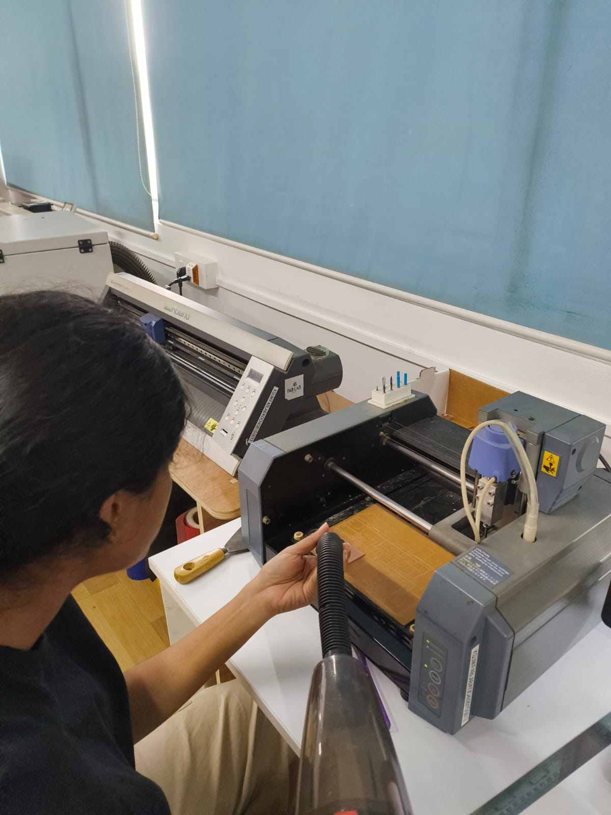
Milling the Board
The FR1 board was taped down flat to the sacrificial bed with double-sided tape across the full surface. Flatness really does affect trace quality, so I pressed it down evenly before starting.
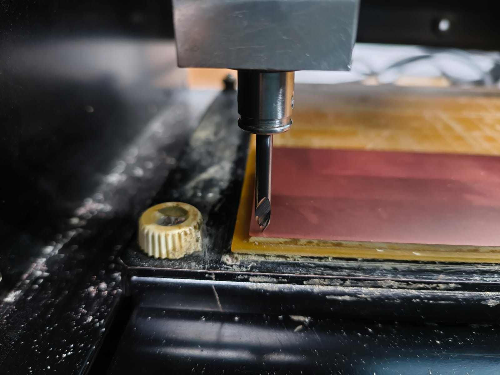
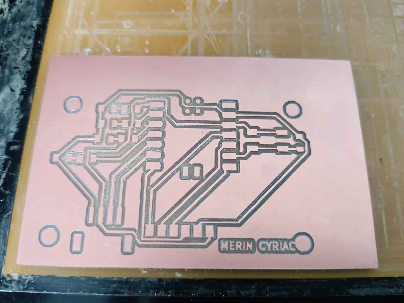
Once the traces were done, I swapped to the 1/32" (0.8 mm) end mill and ran the drills, then the board outline. Same process: re-zero Z, open socket, send file.
Step 4
Soldering Components
With the board milled and sanded, I proceeded to solder the components into it.
Sourcing Components from FabStash
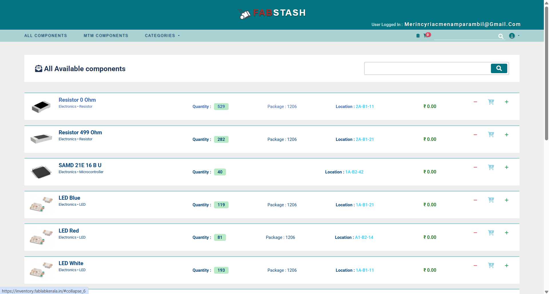
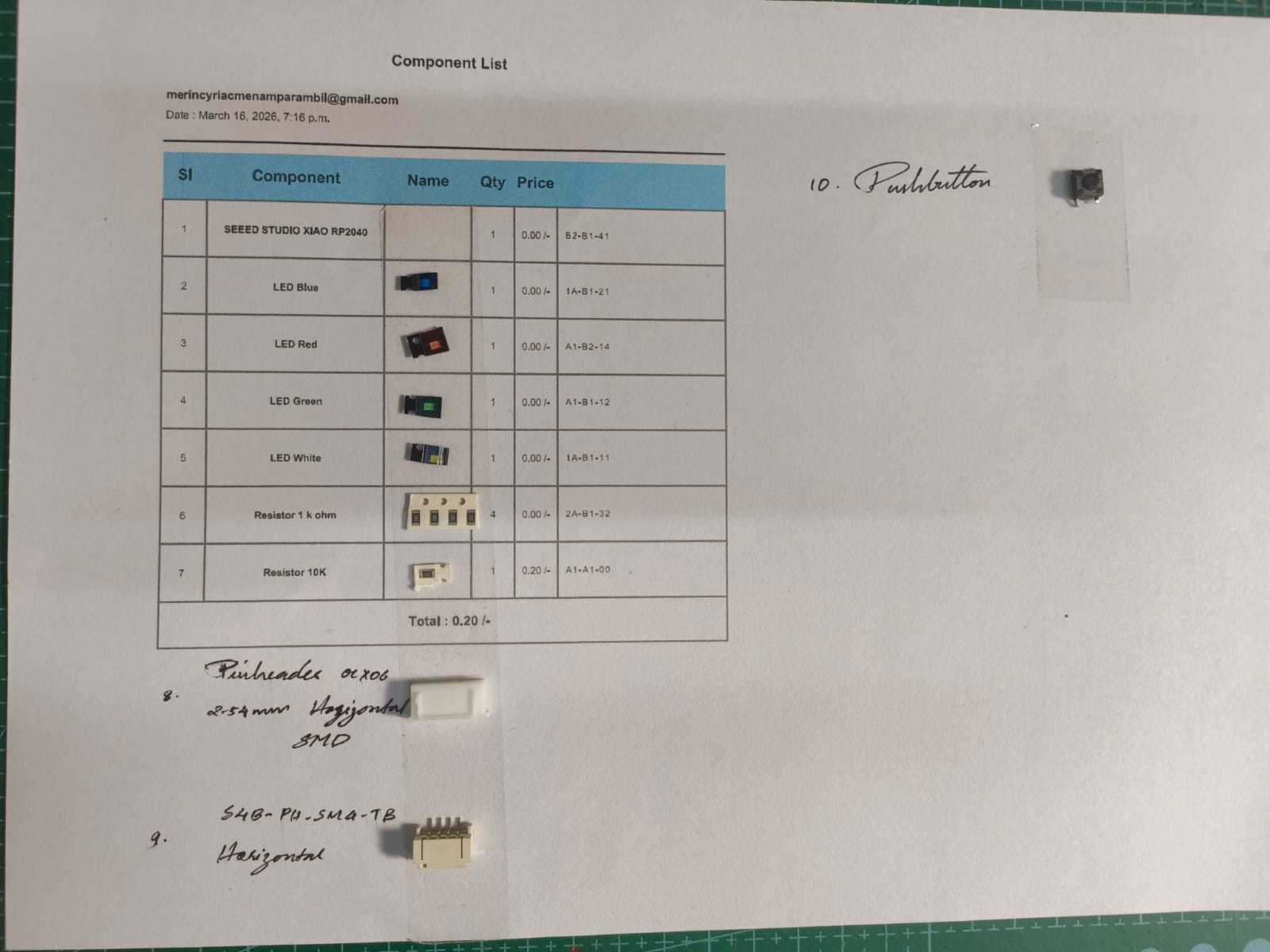
All components were sourced from FabStash — Fab Lab Kerala's in-house component inventory and management system. FabStash provides a searchable catalogue of lab-stocked parts complete with datasheets, package types, and live stock levels, making it straightforward to locate and verify exactly what is needed for a design without waiting for external procurement.
The FabStash inventory is accessible at inventory.fablabkerala.in.
In Fabstash, you can search for the components you need, and add them to the cart. Once you have added all the components you need, you can click 'Request' and the components will be reserved for you.
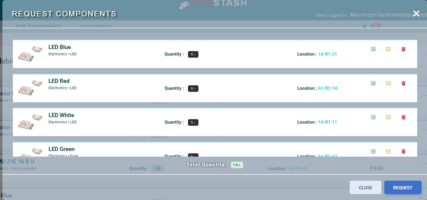
After you click 'Request', you can click the clipboard icon and see the pending request you send to the lab.
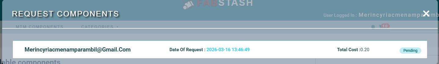
You can click on the request and then you can see the components you requested. At the bottom right corner, there is a button to print the file. Click it and print the file.
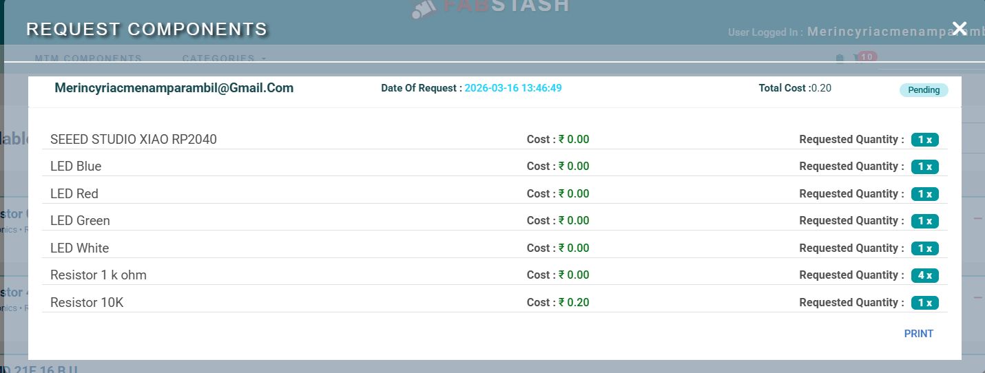
After you print out the request, you can take the components from the Academy inventory and attach them to the corresponding component name.
Soldering Process
Before soldering, each component footprint on the board was verified against its physical package to confirm correct orientation and pin assignment. The 0402 passive components (resistors and LED) were placed under a soldering microscope for precision work.
For each SMD component, my process was:
- Apply a small amount of liquid flux to both pads
- Tin one pad lightly with solder
- Place the component with reverse-action tweezers and tack it to the tinned pad
- Solder the second pad with fresh solder and a clean iron tip
- Return to the first pad to reflow and form a proper fillet joint
- Clean the area with IPA flux remover
The XIAO RP2040 module was soldered last — its castellated pads were first pre-tinned, then aligned to the board footprint and reflowed carefully to avoid cold joints or bridging between adjacent pads.
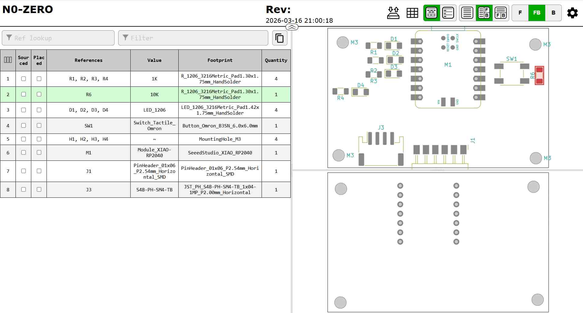
Verifying Components with the KiCad BOM Plugin
Before picking up the soldering iron, I cross-referenced the physical components against the design's Bill of Materials (BOM) using KiCad's built-in BOM plugin. The plugin reads the schematic's component annotations and outputs a structured list of every part — reference designator, value, package, and quantity — making it straightforward to confirm that nothing is missing and that every component matches the correct footprint before committing to solder.
This step catches mismatches early: a 10 kΩ resistor placed where a 1 kΩ is expected, or an 0603 package in a footprint designed for 0402, are both far easier to catch on the BOM list than to diagnose on a soldered board.
The InteractiveHtmlBom plugin (ibom) is a KiCad add-on that generates a self-contained HTML file combining a filterable component table with a live, clickable PCB view. Hovering or clicking a component in the table highlights its exact location on the board, making it far easier to find small 0402 passives during hand-assembly than working from a static reference designator list.
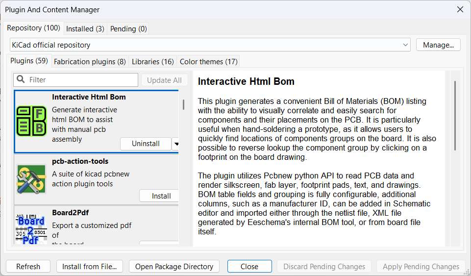
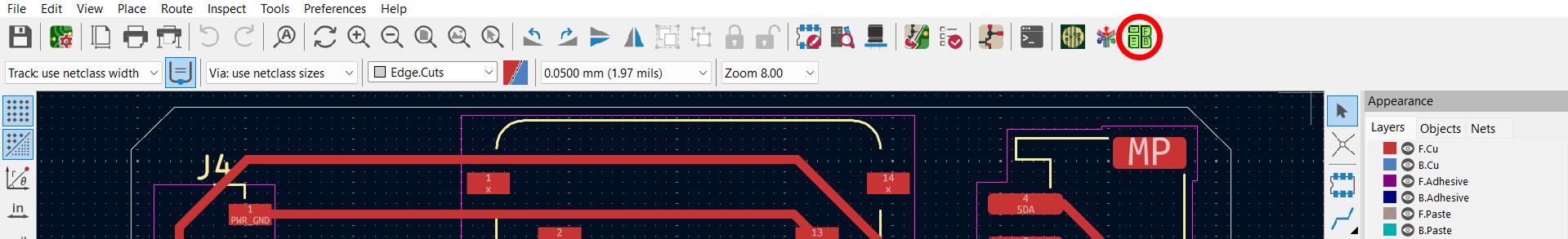
With the board open in KiCad's PCB editor, click the ibom icon in the toolbar (circled below). If the icon is not visible, the plugin must first be installed via the Plugin and Content Manager in the same way as the Gerber2PNG plugin described earlier.
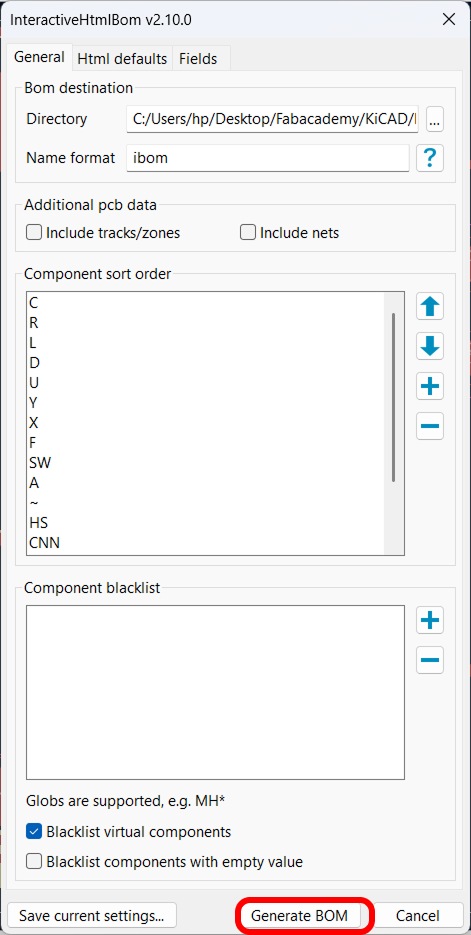
Clicking the icon opens the InteractiveHtmlBom v2.10.0 settings dialog. The key options configured here were:
- BOM destination — output directory where the HTML file will be saved
- Name format — set to
ibom, producingibom.html - Component sort order — resistors (R) and capacitors (C) listed first, followed by LEDs (D), ICs (U), and switches (SW)
- Blacklist virtual components — checked, so mechanical mounting holes and test points are excluded from the BOM table
Once the settings are confirmed, clicking Generate BOM produces the HTML file and opens it in the default browser.
The generated ibom.html opens as a two-panel browser view. The left panel
contains a filterable table listing every component — reference designator, value,
footprint, and quantity. The right panel shows an interactive rendering of the PCB.
Clicking any row in the table highlights the corresponding component pads on the board
in real time, which made placing and verifying each 0402 component significantly faster
and less error-prone during assembly.
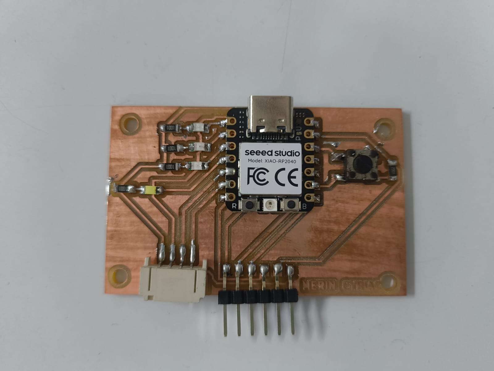
Completed Assembly
With all components soldered, the board was complete. Working outward from the centre:
- Seeed Studio XIAO RP2040 — mounted centrally, USB-C port facing up, castellated pads reflowed flush to the board footprint
- 0402 passive components — SMD resistors and LED arranged to the left of the XIAO; all joints checked under the microscope for clean fillets with no bridging
- Tactile push button — placed to the right of the XIAO, used as the user input for speed control in the firmware
- JST connector — bottom-left, providing an alternative power input path
- Pin headers — bottom-right, breaking out the XIAO's GPIO pins for prototyping and external connections
The milled copper traces are clearly visible through the gaps between component pads, confirming no accidental copper bridging occurred during soldering. The board was now ready for the pre-power inspection and functional test described in the next step.
Step 5
Testing the Board
Before applying power, I performed a thorough pre-power inspection:
- Visual inspection — checked every solder joint under the microscope for cold joints, bridges, or lifted pads
- Continuity check — probed VCC and GND rails to confirm no short circuit existed between them
- Net connectivity — verified key signal nets (LED pin, button pin, XIAO I/O) were connected as designed
The board passed all pre-power checks. I connected it to a PC via USB-C. The XIAO RP2040 was recognised immediately as a USB device, confirming the board's power rails were clean and the microcontroller was functional.
Step 6
Programming Environment Setup
With the board tested and confirmed functional over USB, the next step was to configure a programming environment and write firmware.
Configuring the Arduino IDE for the XIAO RP2040
The XIAO RP2040 is not included in the Arduino IDE's default board list and requires a third-party board package to be added manually. Follow the steps below to prepare the IDE:
- Open the Arduino IDE and navigate to File → Preferences.
-
In the Additional Board Manager URLs field, paste the following URL
and click OK:
https://github.com/earlephilhower/arduino-pico/releases/download/global/package_rp2040_index.json - Navigate to Tools → Board → Board Manager, search for Raspberry Pi Pico/RP2040, and click Install. This installs the full RP2040 board family including the XIAO variant.
- Once installed, select the target board via Tools → Board → Raspberry Pi RP2040 Boards → Seeed XIAO RP2040.
- Connect the board via USB-C, select the correct port under Tools → Port, and click Upload to flash a sketch.
Christmas Lights
To demonstrate the board's capabilities, I wrote a Christmas lights animation program that drives four LEDs through a sequence of patterns. The program also accepts input from the tactile push button to cycle through animation speeds at runtime, making it an interactive demonstration of both digital output and digital input on the XIAO RP2040.
Program Behaviour
Each iteration of loop() runs through four distinct LED animation patterns
in sequence:
- Chase forward — LEDs light up one at a time from D0 to D3, creating a left-to-right sweep
- Chase backward — the same sweep runs in reverse, from D3 back to D0
- Fill and empty — LEDs accumulate one by one until all four are lit, then extinguish in reverse order
- Blink all — all four LEDs flash on and off together three times
The timing of every animation step is governed by a single delayTime variable
(initialised to 150 ms). Pressing the push button increments this value by 50 ms,
slowing the animation, and wraps back to 50 ms once it exceeds 400 ms, cycling
through five distinct speed levels.
Complete Code
// Christmas Lights — XIAO RP2040
// Cycles through four LED animation patterns.
// Tactile button press increments animation speed.

const int ledPins[]  = {D0, D1, D2, D3};
const int NUM_LEDS   = 4;
const int BUTTON_PIN = D8;

int delayTime = 150;  // ms between each animation step

void setup() {
  for (int i = 0; i < NUM_LEDS; i++) {
    pinMode(ledPins[i], OUTPUT);
    digitalWrite(ledPins[i], LOW);
  }
  pinMode(BUTTON_PIN, INPUT_PULLUP);  // active-low with internal pull-up
}

void loop() {
  // 1 — Chase forward (D0 → D3)
  for (int i = 0; i < NUM_LEDS; i++) {
    digitalWrite(ledPins[i], HIGH);
    delay(delayTime);
    digitalWrite(ledPins[i], LOW);
  }

  // 2 — Chase backward (D3 → D0)
  for (int i = NUM_LEDS - 1; i >= 0; i--) {
    digitalWrite(ledPins[i], HIGH);
    delay(delayTime);
    digitalWrite(ledPins[i], LOW);
  }

  // 3 — Fill up then empty
  for (int i = 0; i < NUM_LEDS; i++) {
    digitalWrite(ledPins[i], HIGH);
    delay(delayTime);
  }
  for (int i = NUM_LEDS - 1; i >= 0; i--) {
    digitalWrite(ledPins[i], LOW);
    delay(delayTime);
  }

  // 4 — Blink all together x3
  for (int j = 0; j < 3; j++) {
    for (int i = 0; i < NUM_LEDS; i++) digitalWrite(ledPins[i], HIGH);
    delay(delayTime);
    for (int i = 0; i < NUM_LEDS; i++) digitalWrite(ledPins[i], LOW);
    delay(delayTime);
  }

  // Button press cycles speed: 50 → 100 → ... → 400 → 50 ms
  if (digitalRead(BUTTON_PIN) == LOW) {
    delayTime += 50;
    if (delayTime > 400) delayTime = 50;
    delay(300);  // software debounce
  }
}Interrupt-Driven Button Control
With the replacement button soldered cleanly onto the pads, I also rewrote the
button handling in the firmware. The original code read the button pin at the very end of loop() using a simple digitalRead() poll — a press that landed while the animation was mid-pattern would not register until the current pattern finished. The revised version uses a hardware interrupt instead, so every press is captured immediately regardless of where in the animation cycle it occurs.
The program also expands to five animation patterns (up from four), a four-speed mode system (Slow → Medium → Fast → Crazy), and an LED doubling effect in fast modes where two adjacent LEDs light simultaneously to give the illusion of faster movement.
Key Improvements Over v1
-
Hardware interrupt (ISR) —
attachInterrupt()registersbuttonISR()on the falling edge of the button pin. The ISR sets avolatileflag rather than acting directly, keeping the handler as short as possible. -
Interrupt debounce — a 250 ms guard window inside the ISR using
millis()rejects spurious re-triggers caused by contact bounce, with no hardware RC filter needed. -
smartDelay()— replaces every rawdelay()call inside the animation patterns. It breaks the wait into 10 ms slices and callscheckButton()between each slice, so a mode change takes effect within 10 ms rather than waiting for the full animation step to finish. - Mode feedback flash — on each button press, all LEDs extinguish briefly, then (mode + 1) LEDs light up as a visual indicator of the new speed level before the animation resumes.
- LED doubling in fast modes — in modes 2 and 3, the chase patterns simultaneously illuminate two adjacent LEDs, widening the apparent moving block and keeping the animation readable at high speed.
- Pattern 5 — alternating pairs — a new pattern that toggles LEDs 0 & 2 against LEDs 1 & 3, producing a strobe-like effect that intensifies at higher speeds.
Speed Mode Reference
Mode 1 — Medium: 150 ms per step — standard pace.
Mode 2 — Fast: 80 ms per step, LED doubling active, double repetition count on blink and pair patterns.
Mode 3 — Crazy: 40 ms per step, LED doubling active — maximum intensity.
Complete Code
// Christmas Lights v2 — XIAO RP2040
// 4 LEDs, 1 Button | 4 speed modes with interrupt-driven button control

const int ledPins[]  = {D0, D1, D2, D3};
const int NUM_LEDS   = 4;
const int BUTTON_PIN = D8;

volatile bool buttonPressed = false;
int mode      = 0;    // 0=slow  1=medium  2=fast  3=crazy
int delayTime = 300;  // ms per animation step

unsigned long lastDebounce = 0;

// ── Interrupt Service Routine ──────────────────────────────────────────────
// Called instantly on every falling edge of BUTTON_PIN.
// Sets a flag only; never acts directly from within the ISR.
// 250 ms guard window rejects contact bounce without hardware filtering.
void buttonISR() {
  if (millis() - lastDebounce > 250) {
    buttonPressed = true;
    lastDebounce  = millis();
  }
}

// ── Mode change handler ────────────────────────────────────────────────────
// Reads and clears the ISR flag, advances the mode, updates delayTime,
// then flashes (mode+1) LEDs as visual confirmation of the new speed.
void checkButton() {
  if (buttonPressed) {
    buttonPressed = false;
    mode = (mode + 1) % 4;

    switch (mode) {
      case 0: delayTime = 300; break;
      case 1: delayTime = 150; break;
      case 2: delayTime = 80;  break;
      case 3: delayTime = 40;  break;
    }

    // Flash feedback: lit LED count equals current mode index + 1
    for (int i = 0; i < NUM_LEDS; i++) digitalWrite(ledPins[i], LOW);
    delay(100);
    for (int i = 0; i <= mode; i++)    digitalWrite(ledPins[i], HIGH);
    delay(300);
    for (int i = 0; i < NUM_LEDS; i++) digitalWrite(ledPins[i], LOW);
    delay(100);
  }
}

// ── Responsive delay ───────────────────────────────────────────────────────
// Breaks the wait into 10 ms slices so a button press is acted on
// within 10 ms rather than at the end of the full animation step.
void smartDelay(int ms) {
  for (int i = 0; i < ms; i += 10) {
    delay(10);
    checkButton();
  }
}

// ── Setup ──────────────────────────────────────────────────────────────────
void setup() {
  for (int i = 0; i < NUM_LEDS; i++) {
    pinMode(ledPins[i], OUTPUT);
    digitalWrite(ledPins[i], LOW);
  }
  pinMode(BUTTON_PIN, INPUT_PULLUP);
  attachInterrupt(digitalPinToInterrupt(BUTTON_PIN), buttonISR, FALLING);
}

// ── Main loop ──────────────────────────────────────────────────────────────
void loop() {

  // PATTERN 1: Chase forward (modes 2+ light the next LED simultaneously)
  for (int i = 0; i < NUM_LEDS; i++) {
    digitalWrite(ledPins[i], HIGH);
    if (mode >= 2 && i + 1 < NUM_LEDS) digitalWrite(ledPins[i + 1], HIGH);
    smartDelay(delayTime);
    digitalWrite(ledPins[i], LOW);
    if (mode >= 2 && i + 1 < NUM_LEDS) digitalWrite(ledPins[i + 1], LOW);
  }

  // PATTERN 2: Chase backward
  for (int i = NUM_LEDS - 1; i >= 0; i--) {
    digitalWrite(ledPins[i], HIGH);
    if (mode >= 2 && i - 1 >= 0) digitalWrite(ledPins[i - 1], HIGH);
    smartDelay(delayTime);
    digitalWrite(ledPins[i], LOW);
    if (mode >= 2 && i - 1 >= 0) digitalWrite(ledPins[i - 1], LOW);
  }

  // PATTERN 3: Fill up then empty
  for (int i = 0; i < NUM_LEDS; i++) {
    digitalWrite(ledPins[i], HIGH);
    smartDelay(delayTime);
  }
  for (int i = NUM_LEDS - 1; i >= 0; i--) {
    digitalWrite(ledPins[i], LOW);
    smartDelay(delayTime);
  }

  // PATTERN 4: Blink all (6 times in fast modes, 3 in slow/medium)
  int blinkCount = (mode >= 2) ? 6 : 3;
  for (int j = 0; j < blinkCount; j++) {
    for (int i = 0; i < NUM_LEDS; i++) digitalWrite(ledPins[i], HIGH);
    smartDelay(delayTime);
    for (int i = 0; i < NUM_LEDS; i++) digitalWrite(ledPins[i], LOW);
    smartDelay(delayTime);
  }

  // PATTERN 5: Alternating pairs (D0+D2 vs D1+D3)
  int pairCount = (mode >= 2) ? 6 : 3;
  for (int j = 0; j < pairCount; j++) {
    digitalWrite(ledPins[0], HIGH); digitalWrite(ledPins[2], HIGH);
    digitalWrite(ledPins[1], LOW);  digitalWrite(ledPins[3], LOW);
    smartDelay(delayTime);
    digitalWrite(ledPins[0], LOW);  digitalWrite(ledPins[2], LOW);
    digitalWrite(ledPins[1], HIGH); digitalWrite(ledPins[3], HIGH);
    smartDelay(delayTime);
  }
  for (int i = 0; i < NUM_LEDS; i++) digitalWrite(ledPins[i], LOW);
}Key Learnings
- Proper board fixturing — flat double-sided tape and a levelled sacrificial layer — is the single biggest factor in trace milling consistency
- Zeroing the Z-axis precisely on the copper surface is critical; even 0.05 mm error can cause incomplete cuts or substrate damage
- Mods CE's node-based workflow is powerful once understood; the pre-built MDX program makes the learning curve manageable
- Converting to PNG at exactly 1000 DPI ensures the toolpath scaling is accurate in the real world
- Flux application before soldering 0402 SMD components dramatically improves joint quality and reduces bridging
- Always perform a continuity check between power and ground before first power-on — a short can destroy the microcontroller instantly
- FabStash makes component sourcing within the lab efficient and eliminates procurement delays for common parts
Design Files here.