6. Electronics design
Group assignment:
- Use the test equipment in your lab to observe the operation of a microcontroller circuit board(as a minimum, you should demonstrate the use of a multimeter and oscilloscope)
To see our group assignment click here
Individual assignment:
-
Design a development board to interact and communicate with an embedded microcontroller
-
extra credit: try another design workflow; make a case for it; Simulate its operation
PCB Design Documentation
This section outlines the workflow for designing a custom Printed Circuit Board (PCB), from initial schematics to production-ready files.
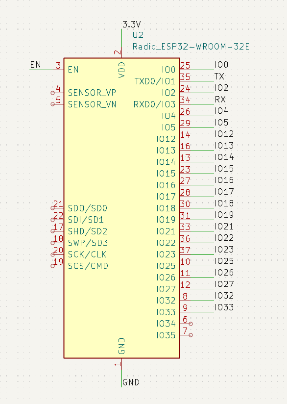
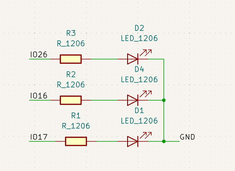
Step 01: Schematic Circuit Design
The first phase involves creating the logical blueprint of the project. This stage defines the electrical connections between components.
-
Component Selection: Choosing symbols and footprints from libraries.
ESP32
-
Electrical Rule Check (ERC): Verifying that there are no disconnected pins or short circuits.
Pro Tip
Always run the ERC (Electrical Rule Check) before moving to the layout phase to avoid logic errors.
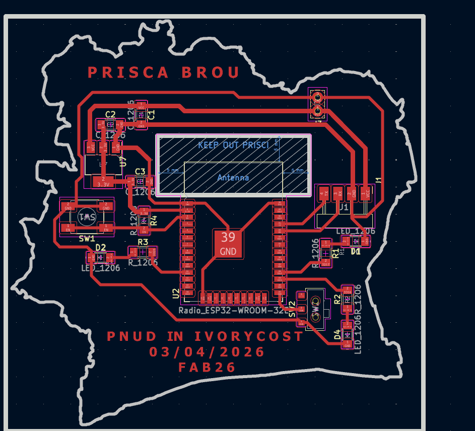
Step 02: Layout Design (Routing)
After validating the schematic, components are placed physically on the board. This is where you define the traces and board characteristics.
- Track Width: Set according to current capacity ( 0.25mm for signals and 0.6mm for power) but in my case use 0.6mm for all.
- Clearance: Maintaining enough space between tracks to prevent interference.
- Pad & Via Diameter: Adjusting sizes for easy soldering and reliable connectivity.
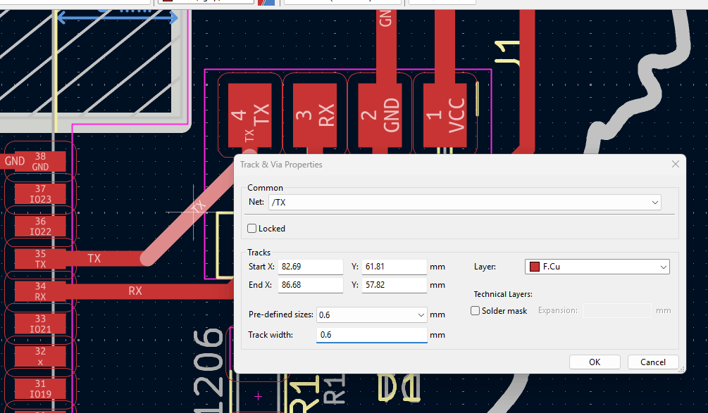
Design Constraints
Ensure the track width is sufficient for the power requirements of your components to prevent overheating.
3D visualize
clix on 3D tool to swich to 3D

results
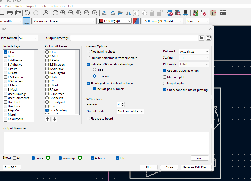
Step 03: Manufacturing File Generation
The final step is to export the design into formats compatible with fabrication machines (CNC or industrial manufacturing).
- dxf Files: Standard files for each layer (Copper, Solder Mask, Silkscreen).
- Excellon Drill Files: Specific data for hole locations and sizes.
- Design Rule Check (DRC): A final automated check to ensure the design matches the manufacturer's capabilities.
Summary Table of Specifications
| Feature | Specification |
|---|---|
| Min Track Width | 0.6 mm |
| Min Clearance | 0.6 mm |
| Via Diameter | 0.6 mm |
| File Format | DXF |