Appearance
Week 6 - Electronics design
Assignments
Group Assignment
- Use the test equipment in your lab to observe the operation of a microcontroller circuit board
Individual Assignment
- Use an EDA tool to design a development board that uses parts from the inventory to interact and communicate with an embedded microcontroller
- Extra credit: try another design workflow
- Eextra credit: simulate your design
- Extra credit: design a case around your design
Group Working
My group work is attached here: https://fabacademy.org/2025/labs/unnc/assignments/week6/week06.html
Individual Working
This week, I plan to design and manufacture an expansion board using Seeed Studio XIAO ESP32-C3, which can accommodate four A4988 stepper motor drivers, enabling independent control of four stepper motors. Through this practice, I will delve into using Fusion 360 for PCB design, covering component selection, schematic drawing, circuit layout optimization, and generating 3D views and manufacturing files to ensure the board’s producibility and stability.
PCB Design Process
Project Initialization
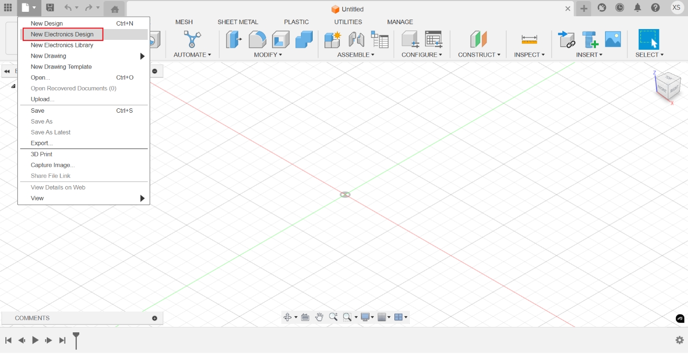
Create a new electronic design project in Fusion 360:
Create a new project and select "New Electronics Design"
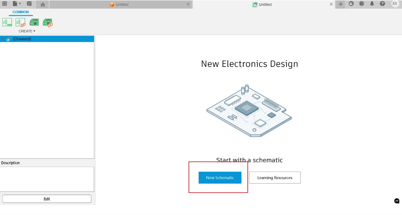
Create a new schematic
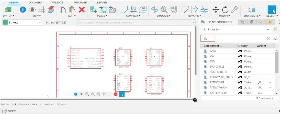
Component Library Preparation
In Fusion 360, I need to use component models for the Seeed Studio Xiao ESP32-C3 and A4988 stepper motor driver. However, as these components were not found in the software, there are two possible solutions:
Manual Component Addition
- Download footprint files from official websites and import existing libraries
Custom Component Design
- Create custom footprints in Fusion 360 and manually draw schematic symbols and PCB layouts
I chose the first approach
Seeed Studio XIAO ESP32-C3
- Download schematic and footprint files from Seeed Studio website
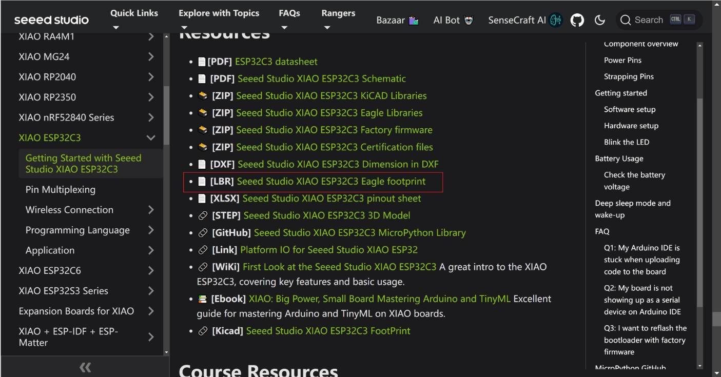
- Import the downloaded .lbr file into Fusion 360
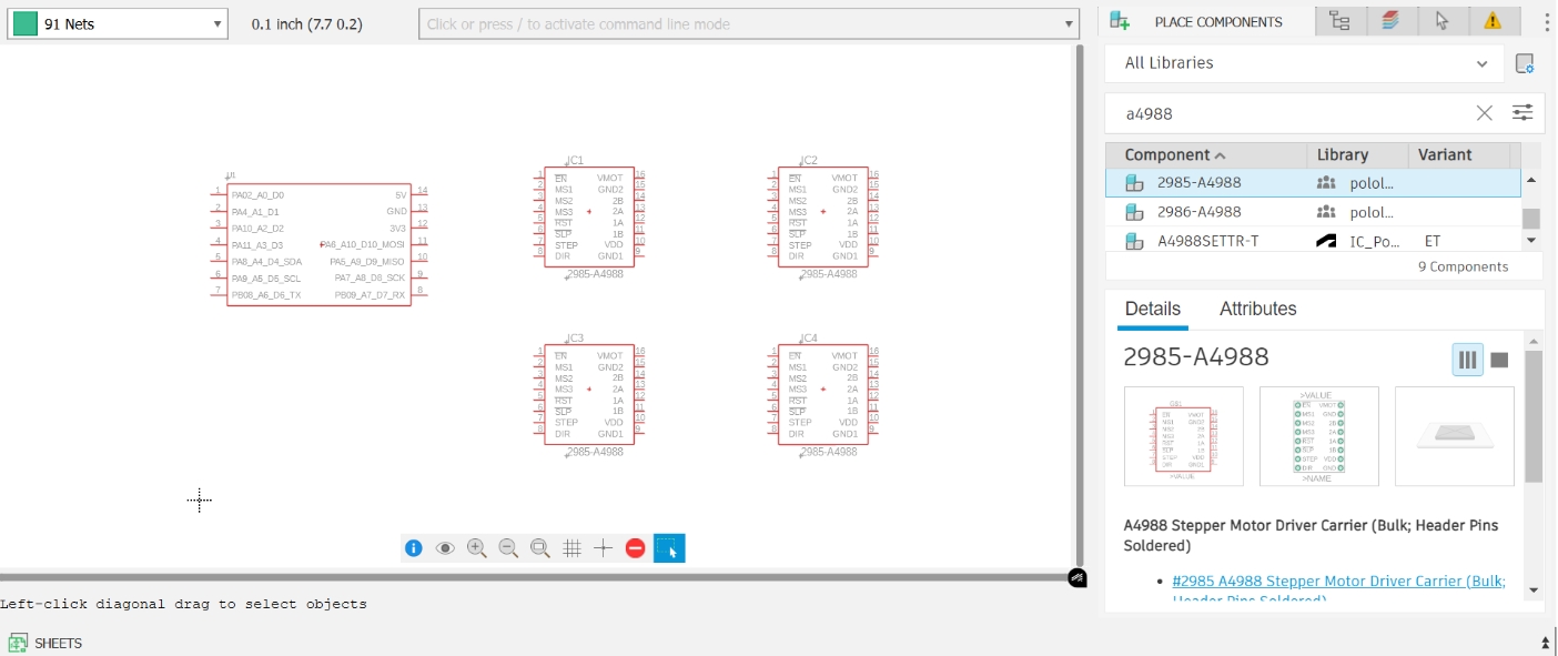
- After successful import, Xiao ESP32-C3 can be found in the component search bar
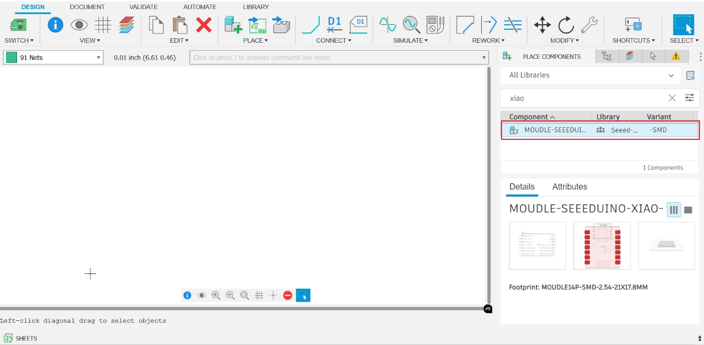
- Click and hold the left mouse button on the desired component, then drag it to the left to place it in the schematic
A4988 Stepper Motor Driver
Obtain the component library file by downloading from GitHub
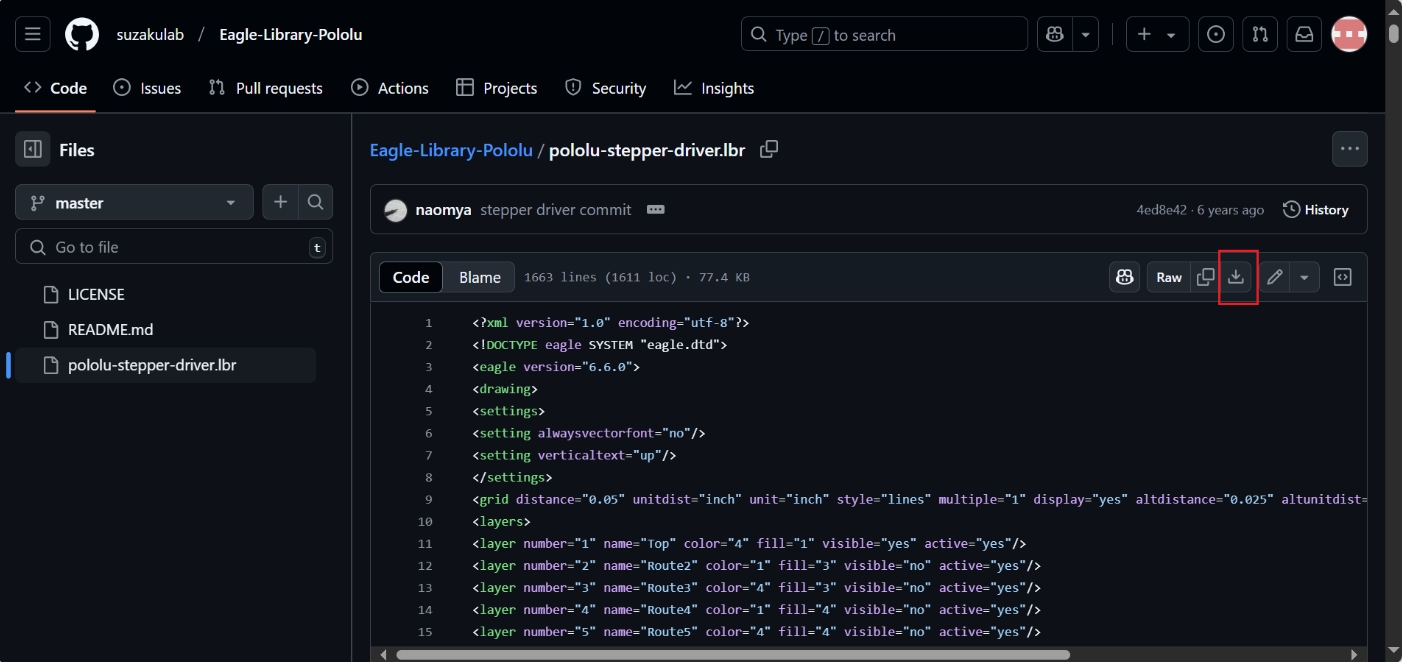 Reference: Eagle-Library-Pololu
Place four A4988 modules in the schematic using the same method
Hardware Specification Analysis
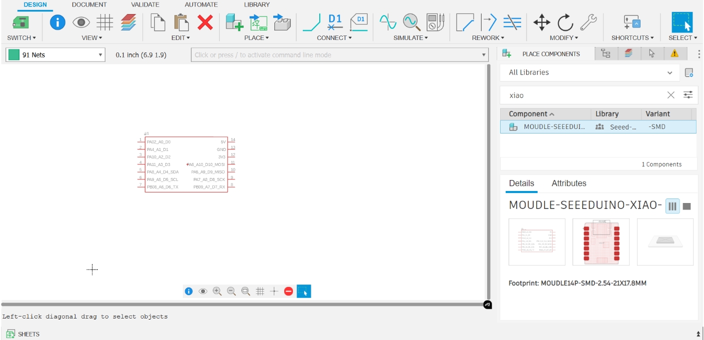
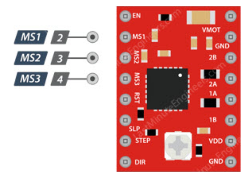
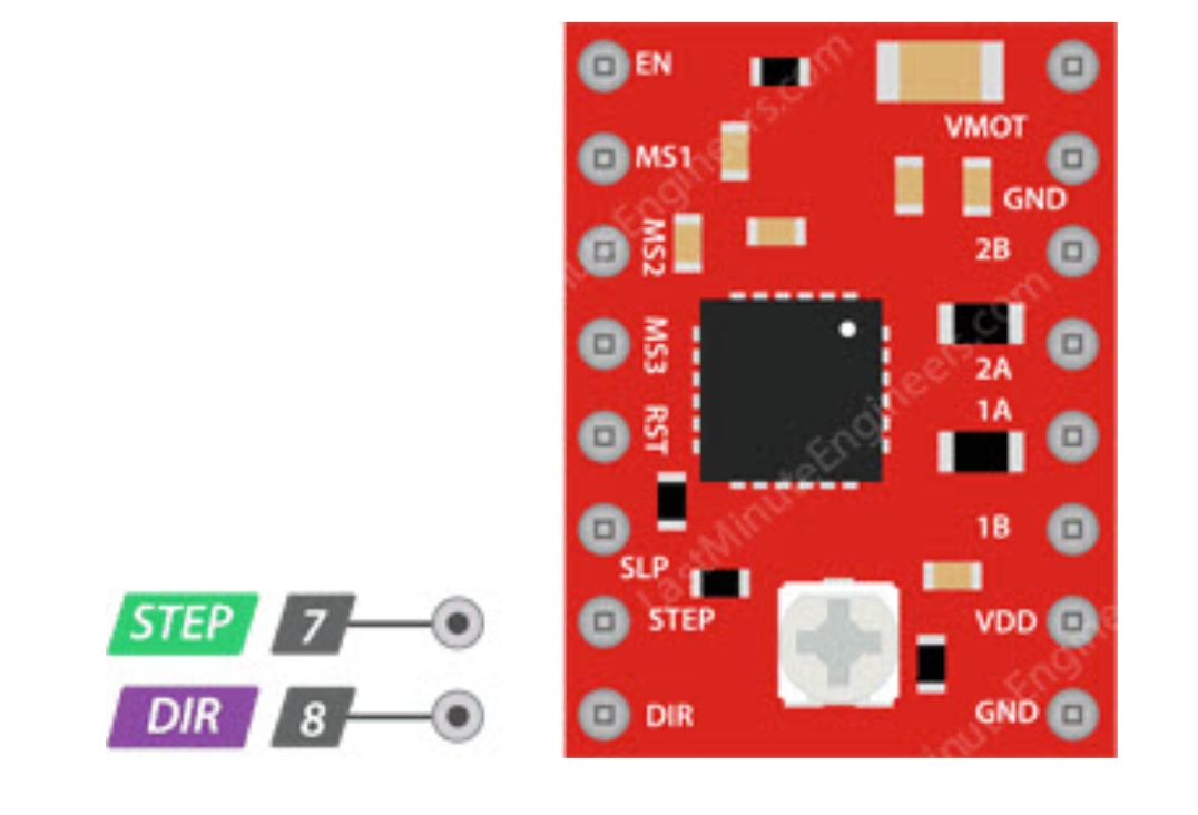
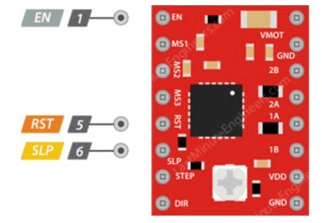
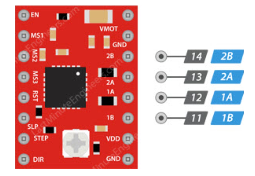
Pin Definitions
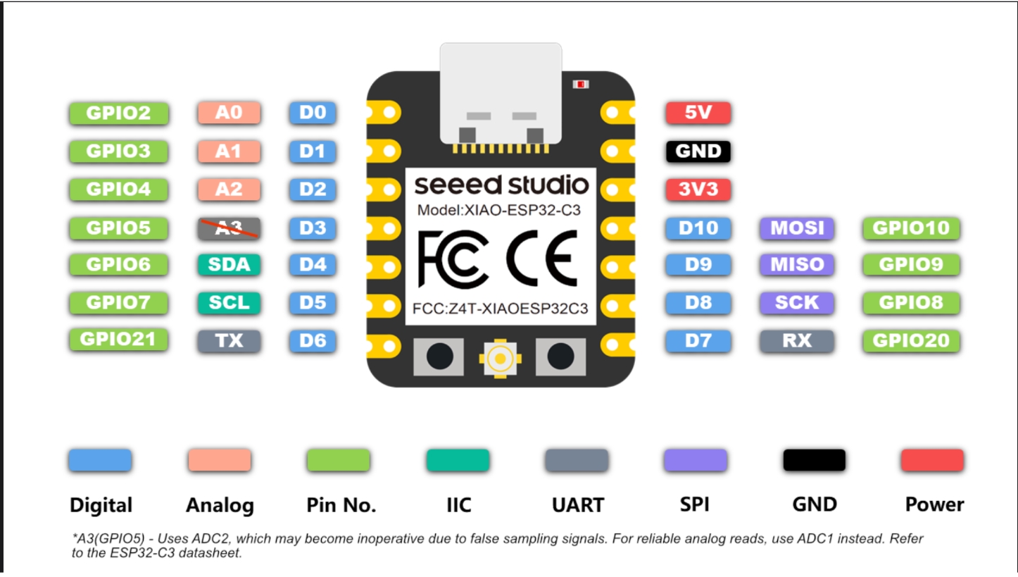
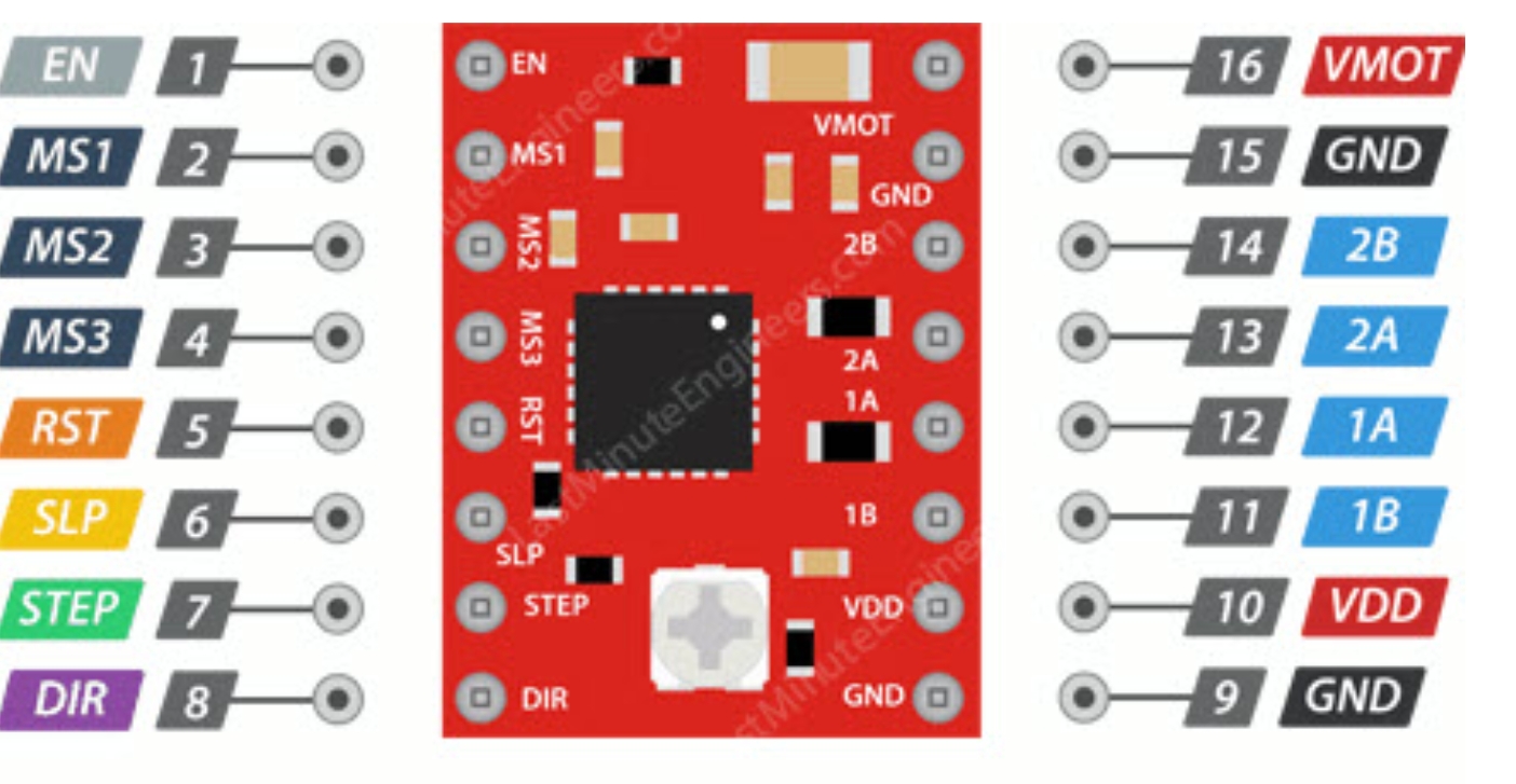
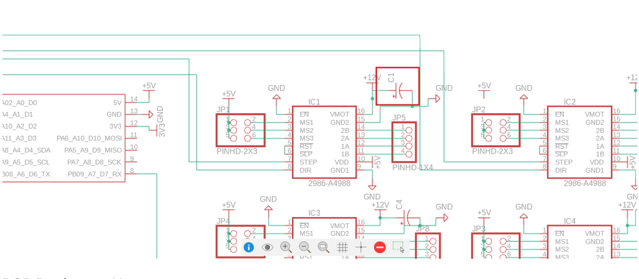
Below are the pin definitions for XIAO ESP32-C3 and A4988. Based on these definitions, I can connect four A4988 modules to the XIAO ESP32-C3 to achieve independent control of four stepper motors.
A4988 Technical Specifications
Here are the technical specifications for the A4988:
| Parameter Type | Specification |
|---|---|
| Motor Output Voltage | 8V – 35V |
| Logic Input Voltage | 3V – 5.5V |
| Continuous Current per Phase | 1A |
| Maximum Current per Phase | 2A |
| Microstepping Resolution | Full, 1/2, 1/4, 1/8, 1/16 |
Power System
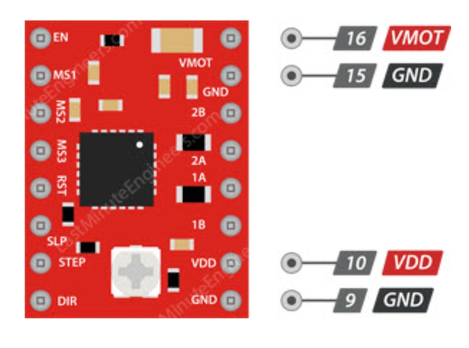
A4988 requires two power connections:
- Logic Power
- VDD-GND: 3V-5.5V, for internal logic circuits
- Motor Power
- VMOT-GND: 8V-35V, for motor drive
- Note: Motor power requires decoupling capacitors to maintain current
Microstepping Control
The A4988 driver supports microstepping, which achieves finer step divisions by applying intermediate current levels to the motor coils.
- MS1/MS2/MS3: Used to select microstepping resolution, different logic level combinations can set different microstepping modes.
- Default state: Pulled down to full-step mode. For example, when driving a NEMA 17 motor (1.8° step angle, i.e., 200 steps/revolution) in quarter-step mode, the motor will execute 800 microsteps per revolution.
Motion Control
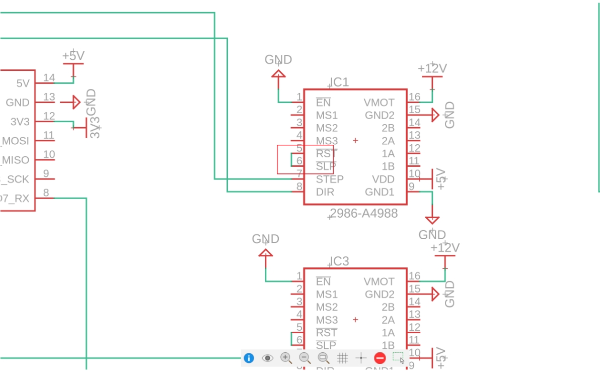
A4988 has two control input pins - STEP and DIR.
- STEP: Step control, each high-level pulse sent to this pin drives the motor according to the microstep selection pins. The faster the pulses, the faster the motor rotates.
- DIR: Direction control, high level for clockwise, low level for counterclockwise
Power Management
- EN: Enable control, default active-low input for this pin
- SLP: Sleep mode, enters on low level
- RST: Reset control, resets on low level
Motor Output
- 1A/1B/2A/2B: Motor phase interfaces for connecting stepper motors.
Pin Assignment Plan
Below is the pin connection plan:
| XIAO ESP32 C3 Pin | Signal Name |
|---|---|
| D0 | Motor 1 STEP |
| D1 | Motor 1 DIR |
| D2 | Motor 2 STEP |
| D3 | Motor 2 DIR |
| D4 | Motor 3 STEP |
| D5 | Motor 3 DIR |
| D6 | Motor 4 STEP |
| D7 | Motor 4 DIR |
| GND | All A4988 ENABLE |
| GND | All A4988 GND |
| 5V | All A4988 VDD |
Circuit Design Implementation
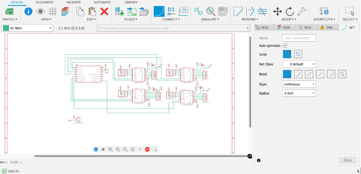
Schematic Design
- Power Area Wiring
First, we wire the power section to ensure proper VCC and GND connections.
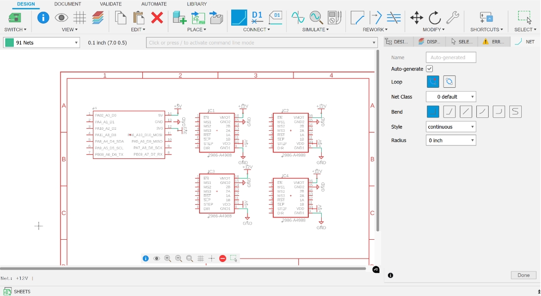 2. Pin Connections
Next, connect the signals between XIAO ESP32 C3 and A4988 stepper motor drivers.
 3. ENABLE Pin Grounding
All A4988 ENABLE pins are connected to GND to enable the stepper drivers by default.
 4. SLP and RST Pin Connection
Connect SLP (Sleep) and RST (Reset) pins together to ensure the driver remains in working state.
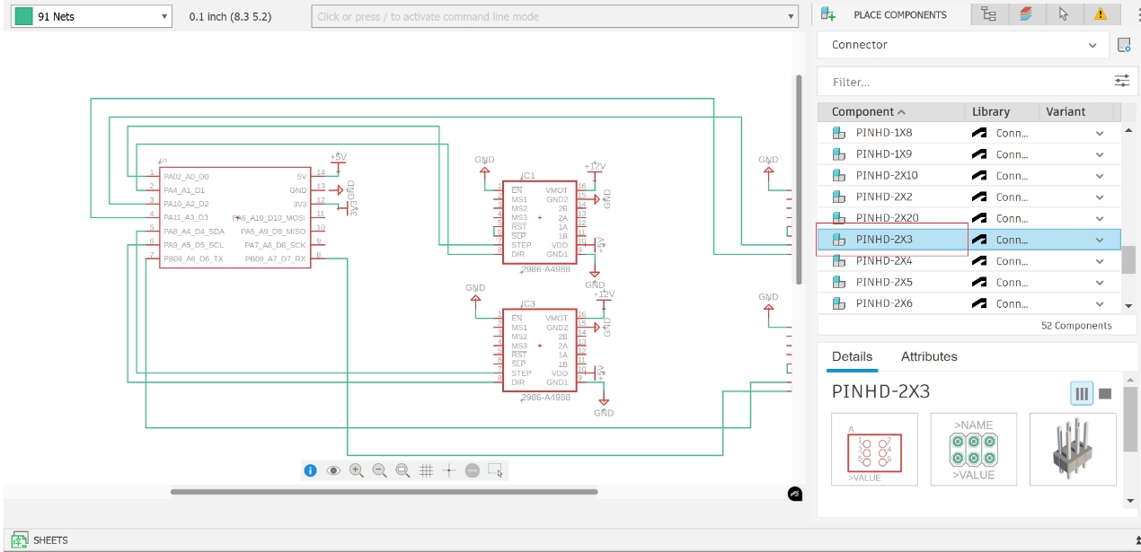
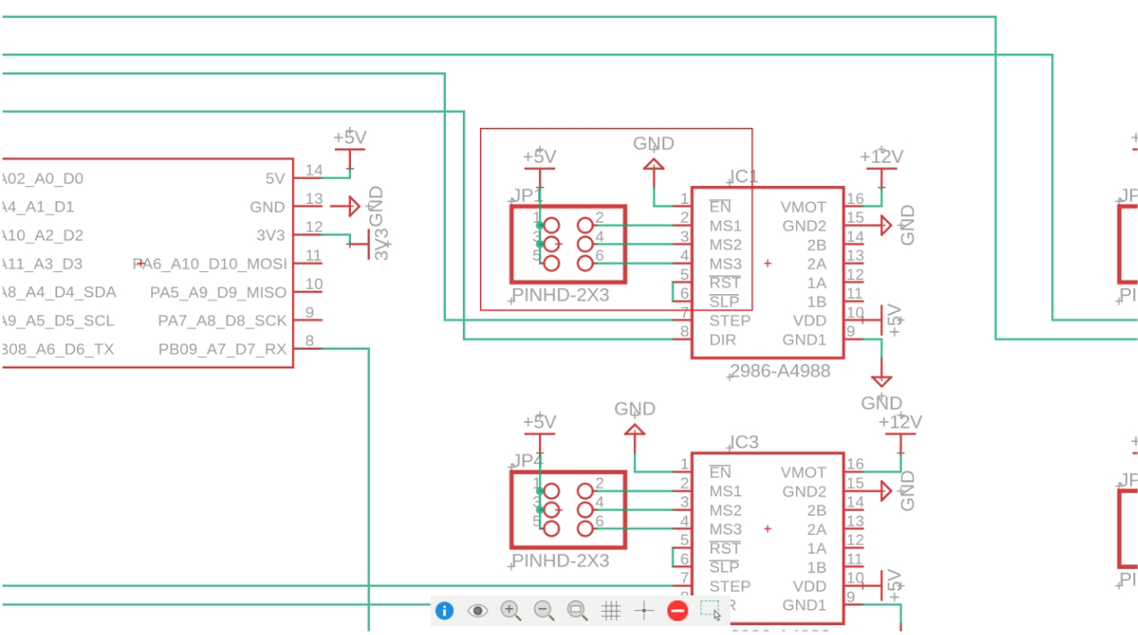
 5. Microstepping Control
A4988 provides MS1, MS2, MS3 microstepping control pins, which we route to dual-row headers with the other end connected to +5V. This allows microstepping mode changes using jumpers.
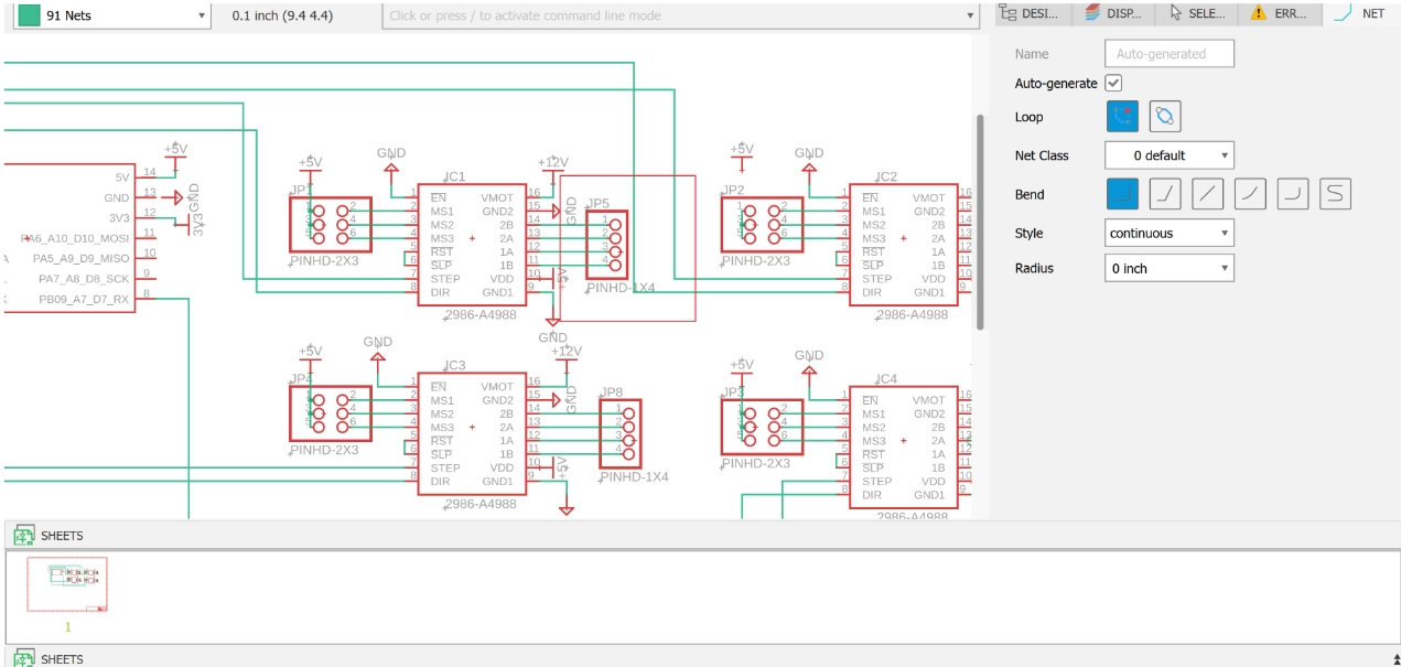
 6. Motor Interface Design
Similarly, we route out the four stepper motor phase signals (1A, 1B, 2A, 2B) for easy connection to external motors.
 To ensure stable motor operation, I added decoupling capacitors in the motor power section to maintain current.
PCB Design and Layout
- Convert to PCB Document
After completing the schematic design, we convert it to a PCB document for board layout.
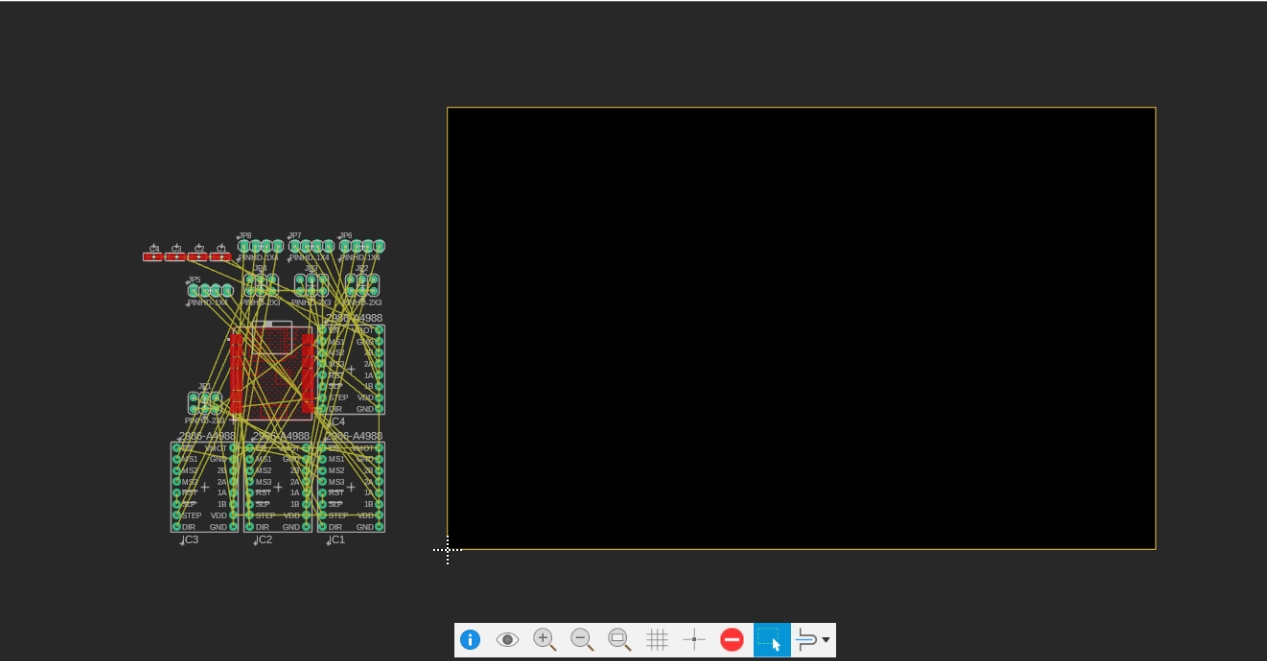 2. PCB Component Arrangement
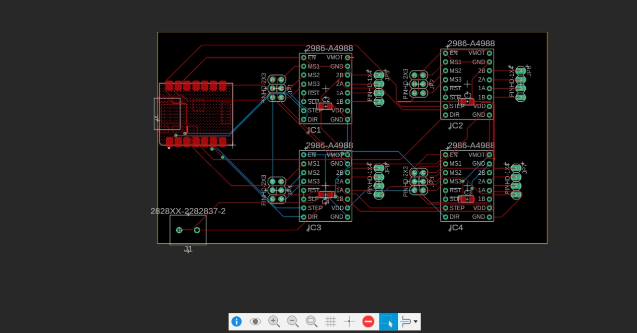
After entering the PCB layout interface, we first arrange the components logically to make the circuit layout clear, compact, and reduce routing complexity.
 3. Routing Complete
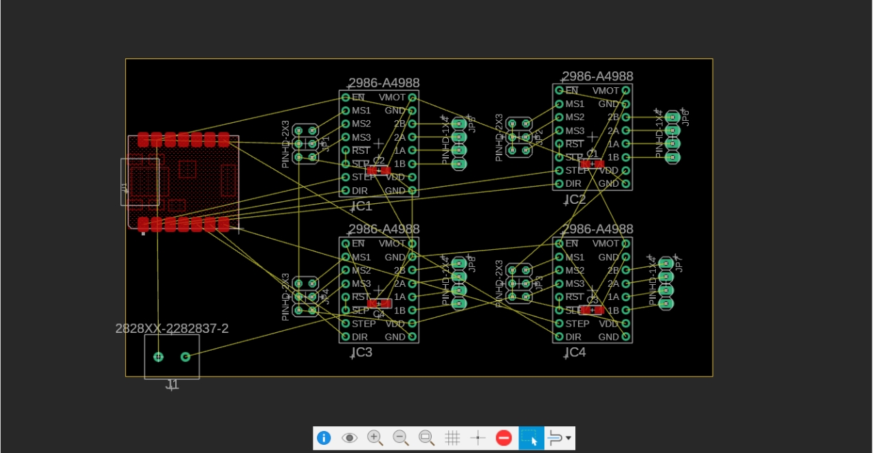
Post-Processing
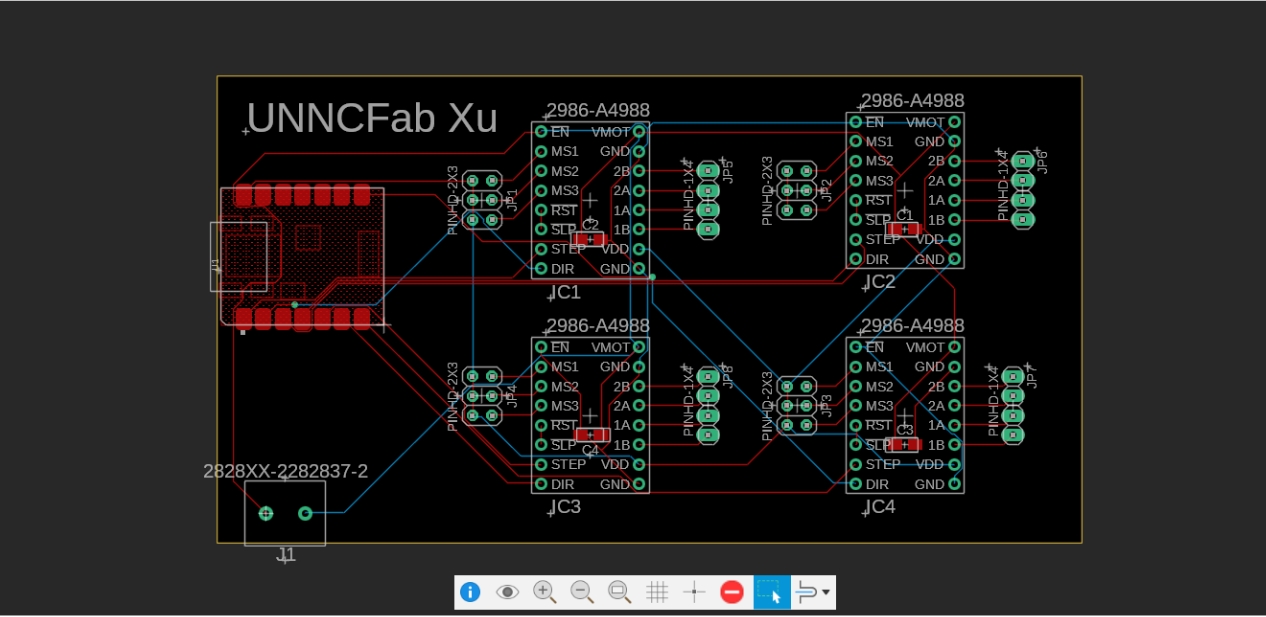
- Add Silkscreen Information
First, select the Top Silkscreen (tSilkS) layer, then add text content (marking pins, module names, etc.).
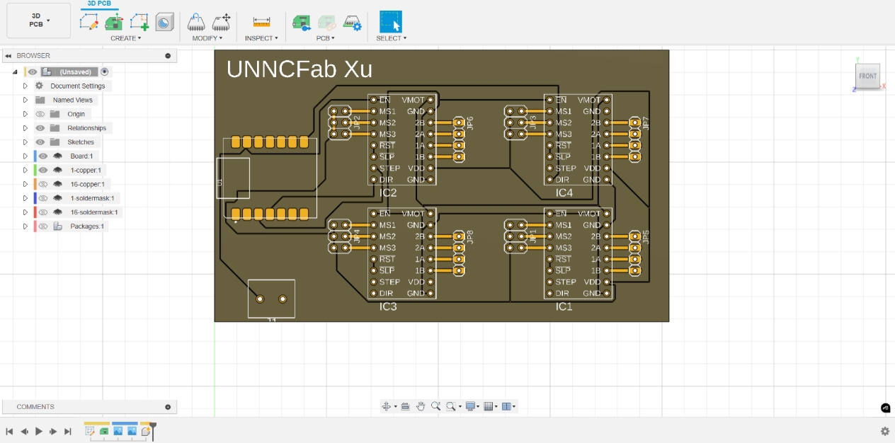
 2. 3D PCB Preview
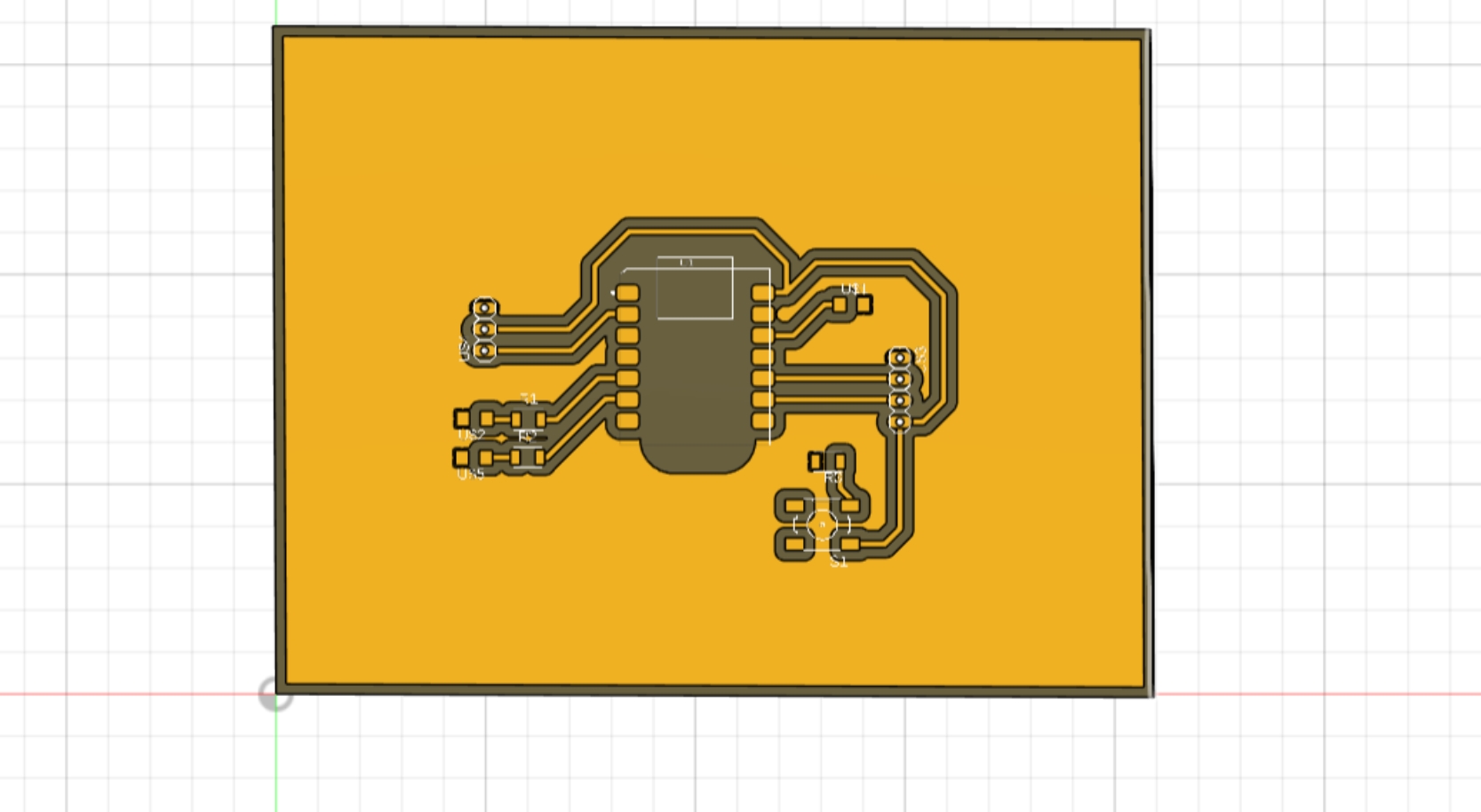
Finally, we push the PCB design to Fusion 360's 3D PCB view to preview the final product appearance.
PCB Design
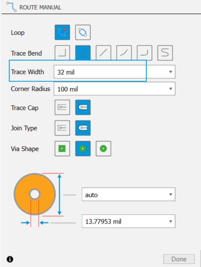
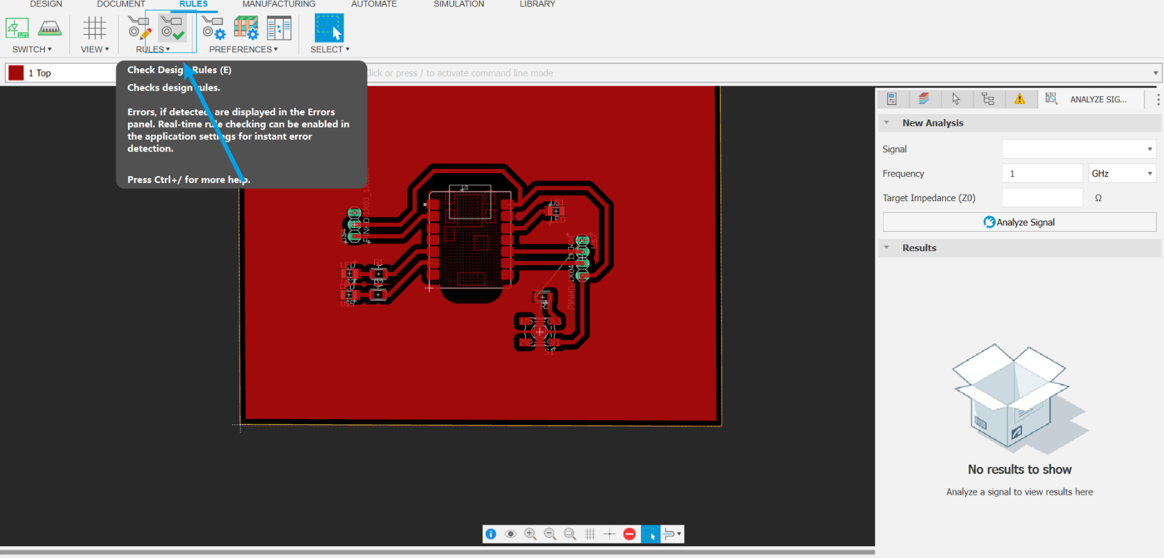
Before processing, the design rules of PCB need to be appropriately adjusted to ensure that it can be used normally after CNC processing and meet actual application requirements.
- Adjust routing rules
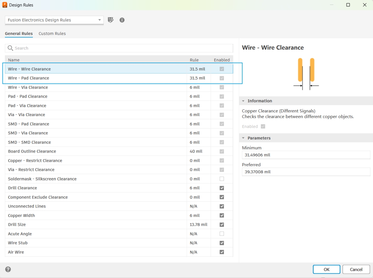 2. Set trace width
- To meet machining requirements, adjust the trace width to 32mil
- The schematic diagram shows XIAO ESP32-C6 interfaces connecting to both ultrasonic and temperature/humidity sensors, with additional LED indicators on D4/D5 for data validation
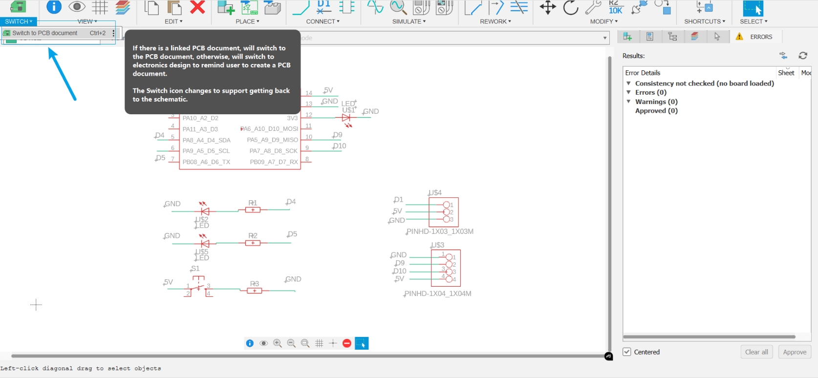
- Switch to PCB document
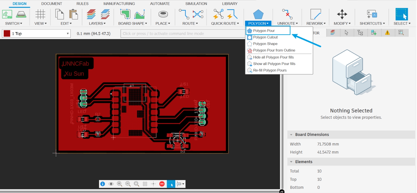
- After the PCB routing was completed, the Polygon Pour operation was performed.
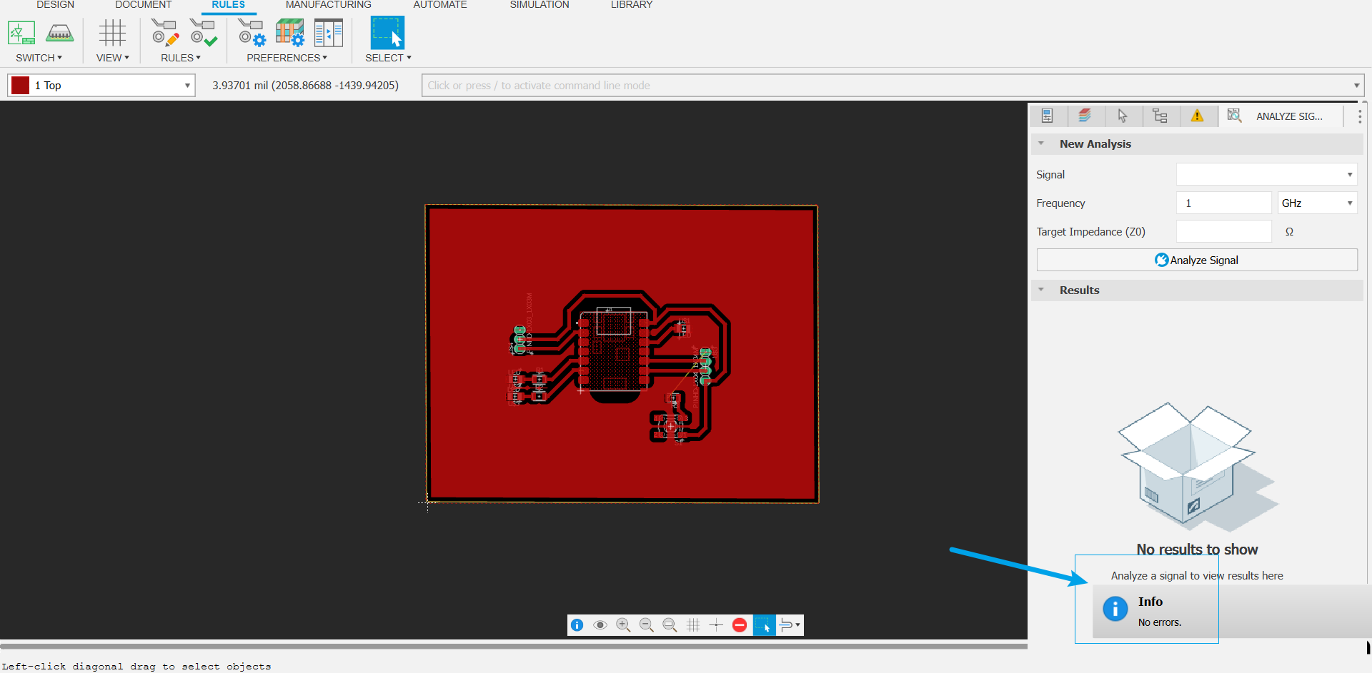
- Check design rules: Since a single-layer board is used, one trace will be connected via a jumper.
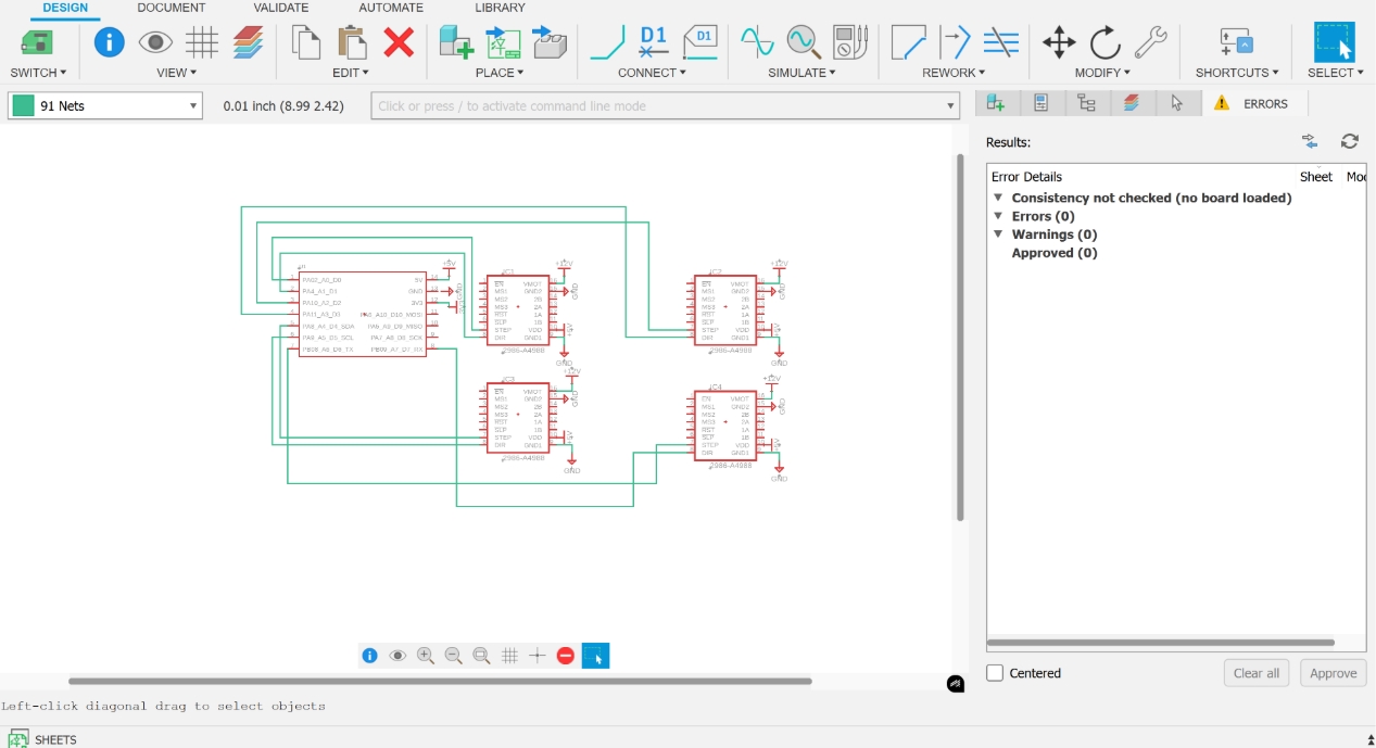
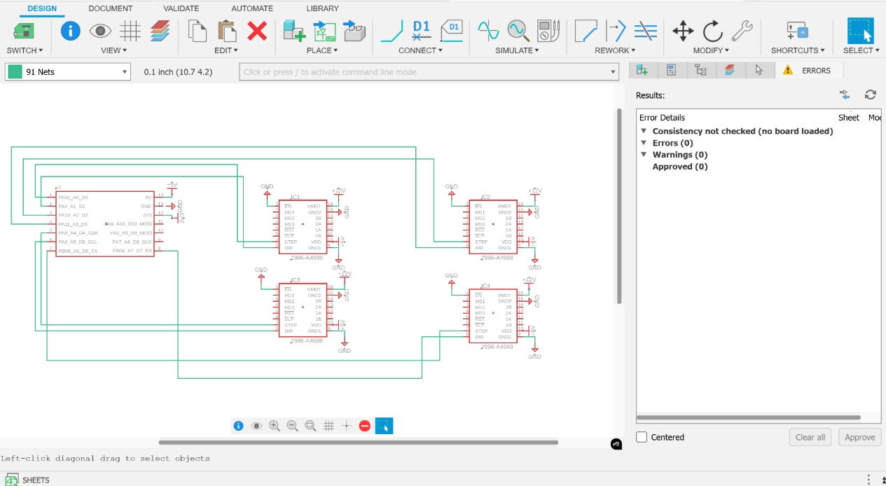
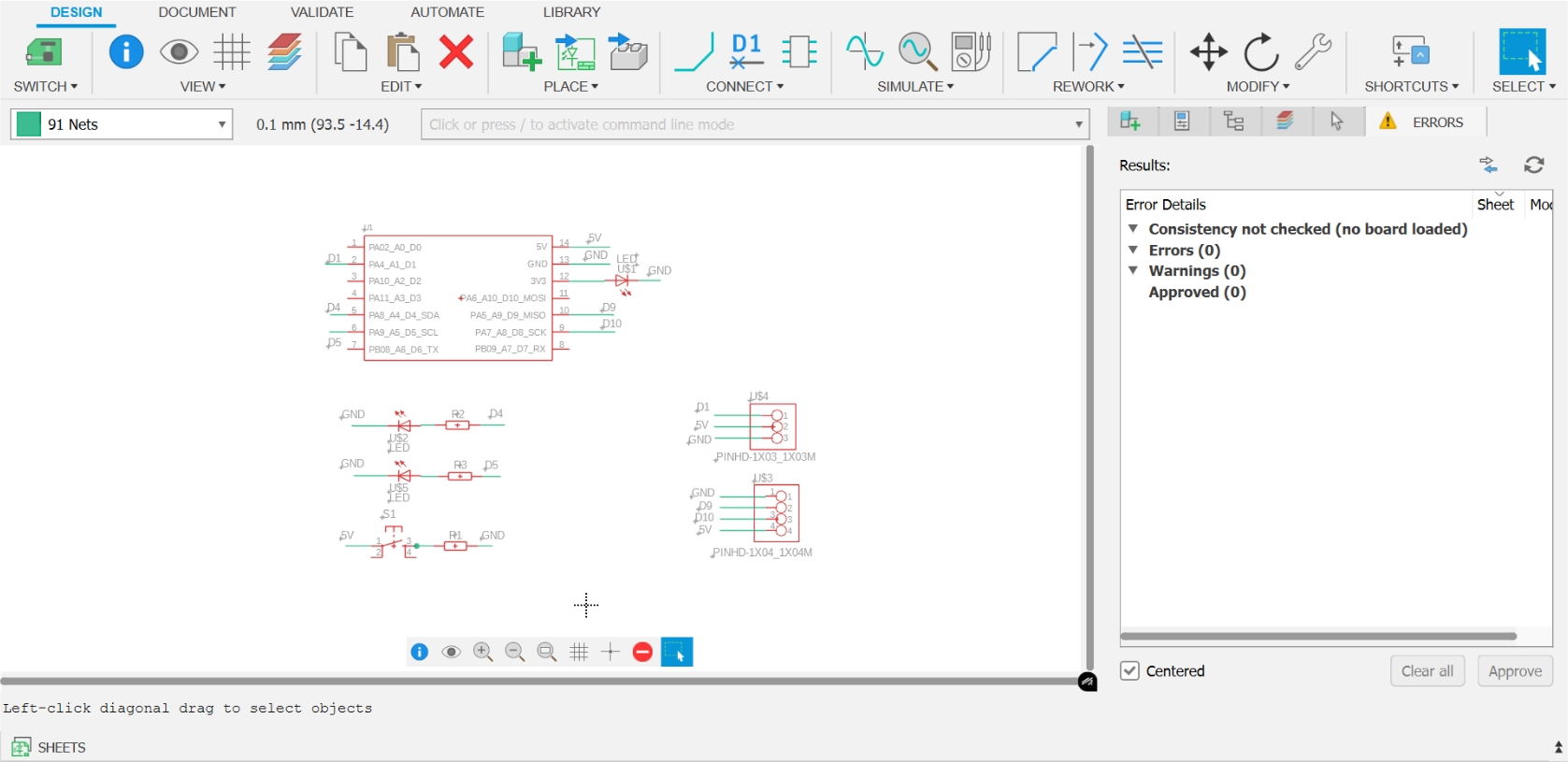
Info no errors
the effect of 3D PCB
 All related files and resources can be found in my Google Drive: https://drive.google.com/drive/folders/1q6vlHqLn06ZCLNSHgEs6LsDOtUmkOZpD?usp=drive_link
Reference:
The reference and design files are listed below:
The .3mf file of PCB Expansion Board 1 can be found in my repository:https://gitlab.fabcloud.org/academany/fabacademy/2025/labs/unnc/students/xu-sun/-/blob/main/docs/assignments/week6/resource-week6/week6-pcbboard1.f3d?ref_type=heads
The .3mf file of PCB Expansion Board 2 can be found in my repository:https://gitlab.fabcloud.org/academany/fabacademy/2025/labs/unnc/students/xu-sun/-/blob/main/docs/assignments/week6/resource-week6/week6-pcbboard2.f3d?ref_type=heads