INPUT DEVICES
GROUP ASSIGNMENTINDIVIDUAL ASSIGNMENT
MOISTURE SENSOR
For this week's assignment we were tasked to measure something, to plug in a sensor to a PCB we have previously designed. For this one I decided to use a moisture sensor which is normally used testing moisture content in the soil.
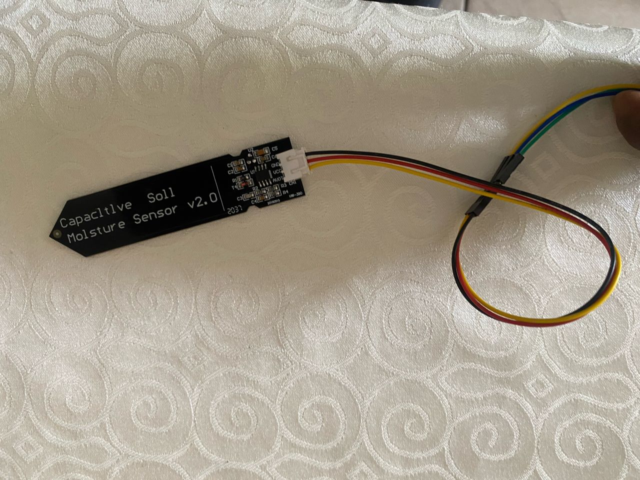
COMPONENTS USED
- PCB (DESIGNED ON WEEK 6)
- JUMPER WIRES
- SOIL MOISTURE SENSOR
I started off by connecting the sensor to analog pins in my board,
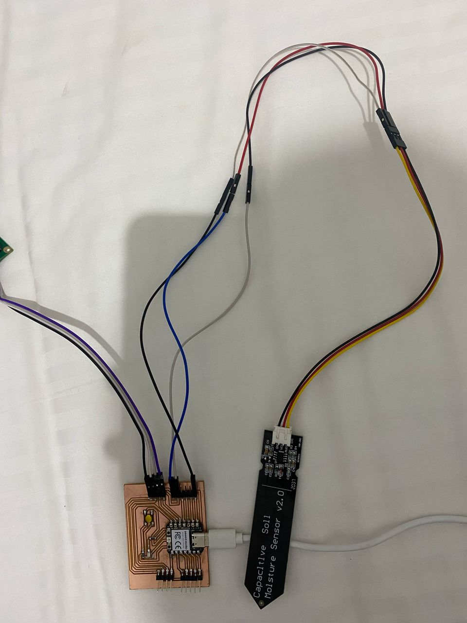
Then Arduino IDE was launched and then programmed the moisture to start taking readings and print them on the serial monitor. The code I used is shown below:
int sensorPin = A0;
int sensorValue;

void setup() {
  Serial.begin(9600);
  pinMode(sensorPin, INPUT);  // Optional; analog pins default to INPUT
}

void loop() {
  sensorValue = analogRead(sensorPin);  // Read the analog value from the sensor
  Serial.print("Moisture Reading: ");
  Serial.println(sensorValue);          // Print the value to Serial Monitor
  delay(1000);                           // Optional: wait 1 second before next read
}
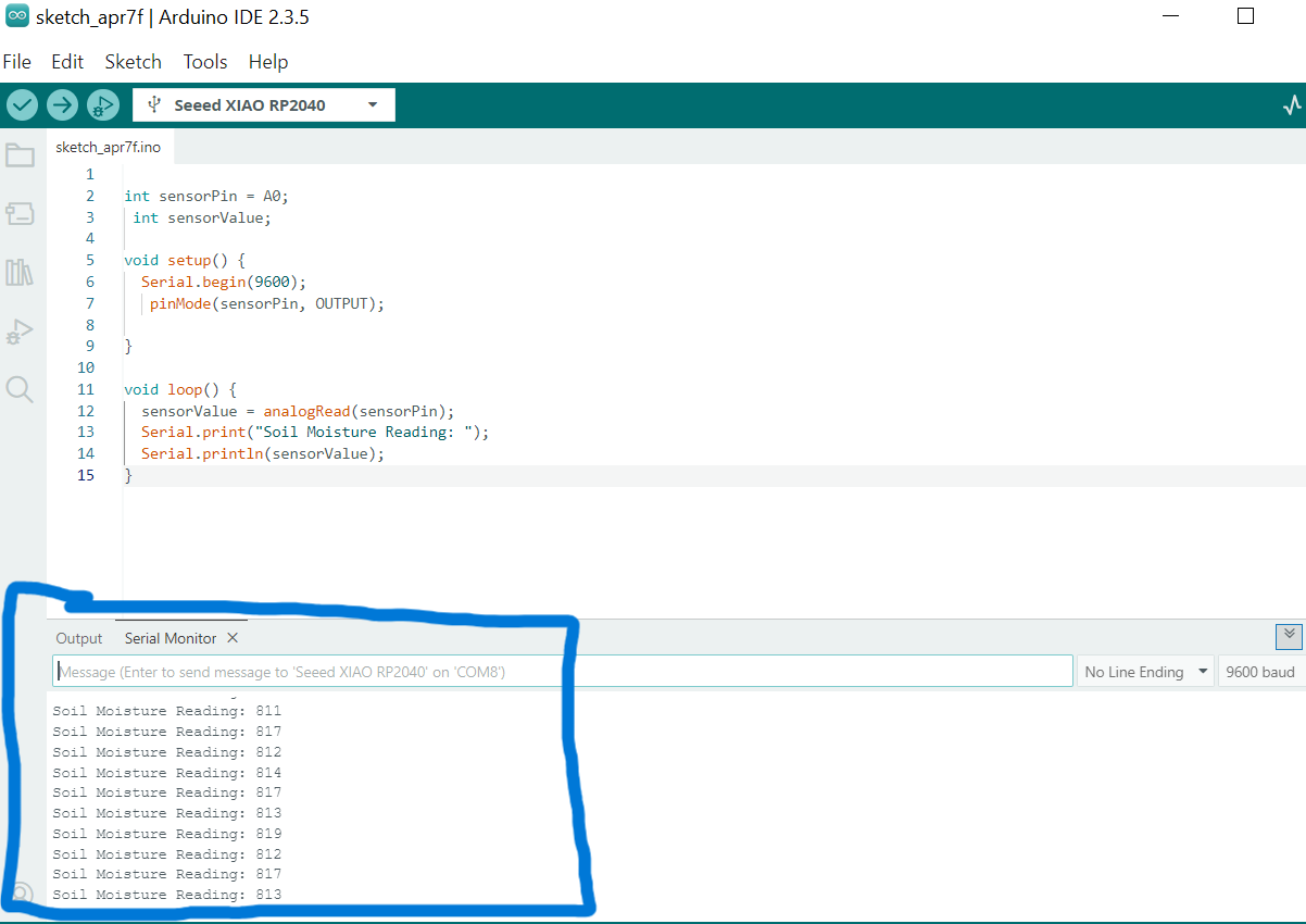
The moisture readings were printed in the serial monitor as shown below:
RFID READER
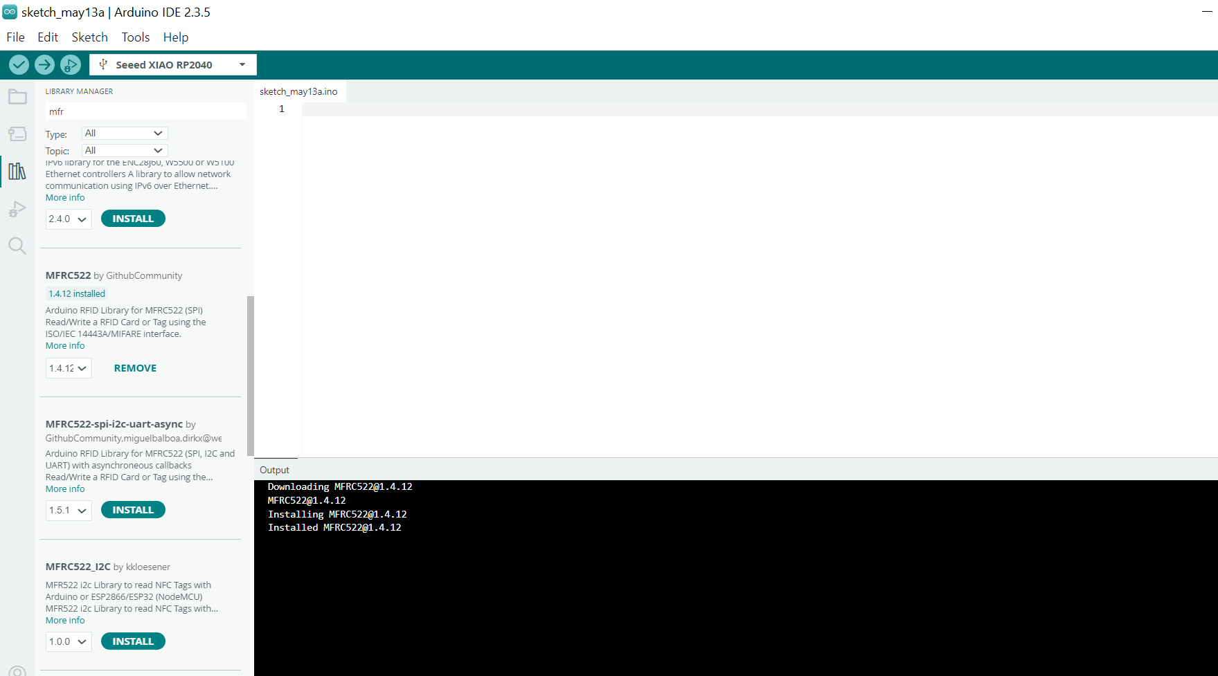
I then tested the digital input using the RFID scanner. The first thing I did was to install the MFRC522 Library into arduino IDE
After that I connected my custom RP2040 xiao board with the RFID reader. The connection is shown below.
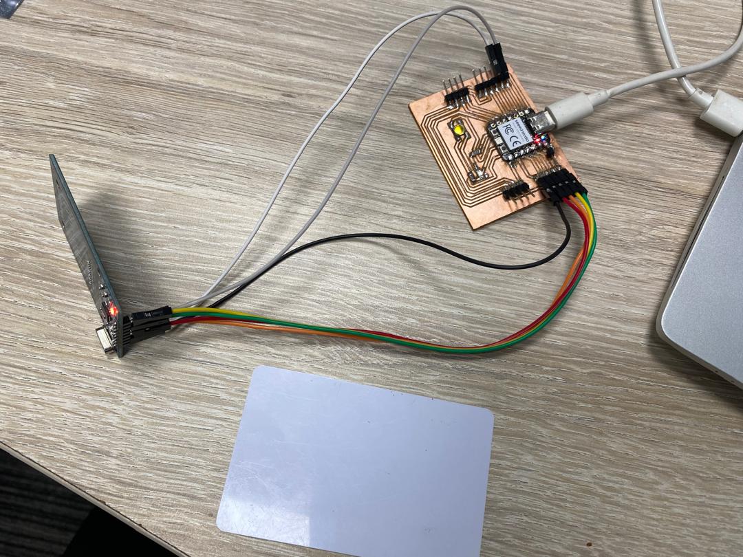
I then went on to code for the RFID reader to reader and display the reading on the serial monitor, and then uploaded it into the board. The code is shown below.
#include < SPI.h>
#include < MFRC522.h>

const int RST_PIN = D0;     // Reset pin
const int SS_PIN = D1;      // SDA

MFRC522 mfrc522(SS_PIN, RST_PIN);   // Create instance

void setup() {
  Serial.begin(9600);
  while (!Serial);  // Wait for Serial Monitor (optional)
  SPI.begin();       // Init SPI bus
  mfrc522.PCD_Init(); // Init MFRC522
  Serial.println("Scan an RFID tag...");
}

void loop() {
  if (!mfrc522.PICC_IsNewCardPresent() || !mfrc522.PICC_ReadCardSerial()) {
    return;
  }

  Serial.print("UID tag: ");
  for (byte i = 0; i < mfrc522.uid.size; i++) {
    Serial.print(mfrc522.uid.uidByte[i] < 0x10 ? " 0" : " ");
    Serial.print(mfrc522.uid.uidByte[i], HEX);
  }
  Serial.println();
  mfrc522.PICC_HaltA();
}
After that I tested it by tapping the cards in the RFID reader and the readings displayed on the serial monitor.
FILES
