ELECTRONICS DESIGN

DEVELOPMENT BOARD DESIGN
The task is to design a development board using Electronic Design Automation (EDA) tools. An EDA tool is software that enables the creation, simulation, and documentation of electronic circuits, making it easier to develop schematics and design Printed Circuit Boards (PCBs). These tools are essential for turning an idea into a functional circuit ready for manufacturing.
KICAD
For this task, KiCad software was used. KiCad is a free, open-source software suite for electronic design automation (EDA), used for designing electronic circuits and printed circuit boards (PCBs).
KICAD BASICS
To design a PCB in KiCad, it is essential to understand its basic elements. Upon opening KiCad, we are presented with a menu that offers various functionalities, such as:
- Schematic Editor
- PCB Editor
- Footprint Editor
- Gerber Viewer
- Image Converter
- Component Calculation Tools
- Worksheet Editor
- Content Plugin Manager
1. GETTING STARTED WITH KICAD
KiCad was first downloaded and installed from its official website.

2. LAUNCHING KICAD
KiCad was launched and a new project was created. The software was downloaded here.
File >> New Project >> Choose folder >> Click save >> open schematic editor

2. ADDITION OF COMPONENTS
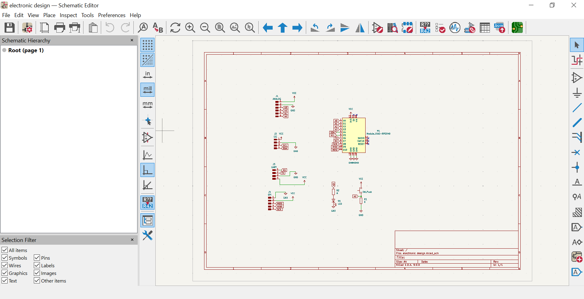
I then used the place symbol tool to place the components of the circuit I am intending to make.
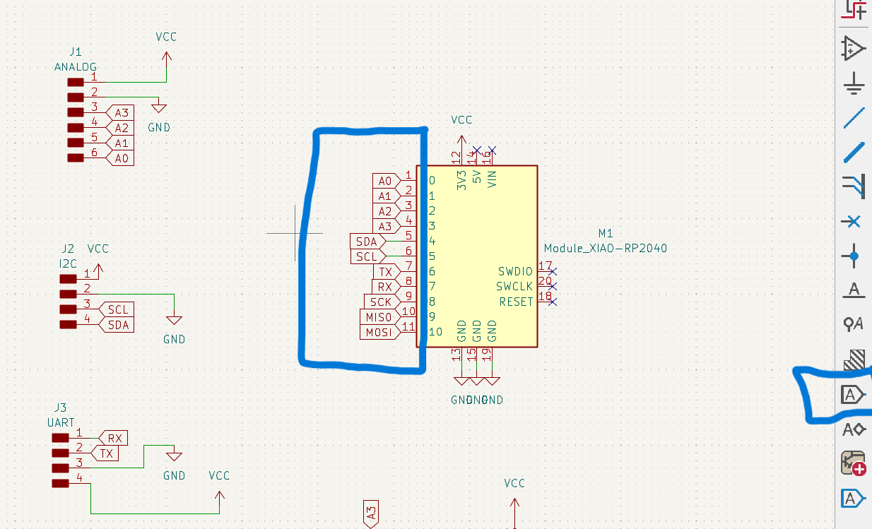
The labelling on the pins was also made using Place Global LAbel tags icon.
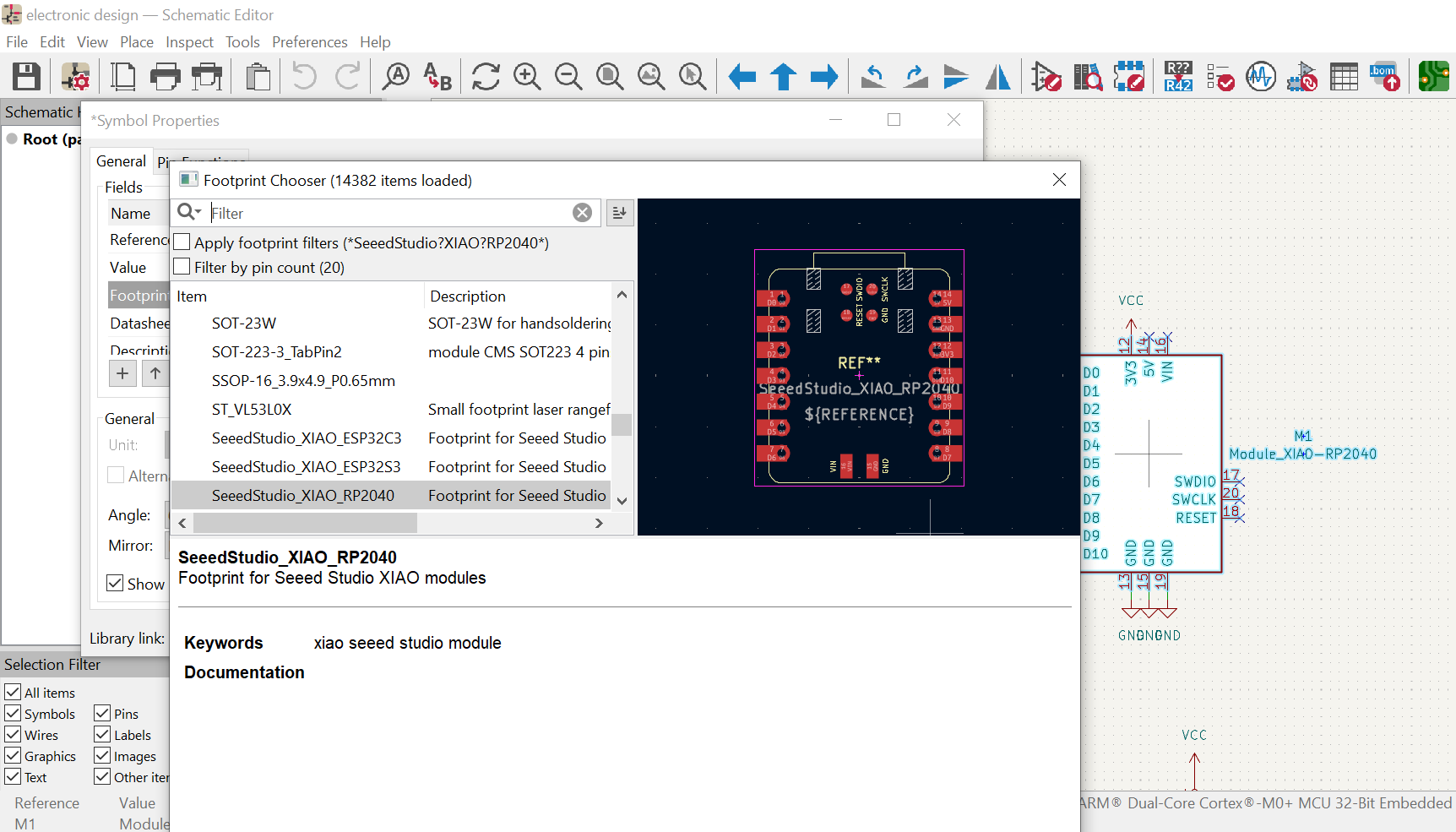
After importing all the components I then assigned ensured that they are all assigned their footprints. I did this by right-clicking on the component and searched for the keyword for the component. This is a critical stage in the design process because footprints define the physical layout of components on a PCB (Printed Circuit Board), including the pad sizes, hole placements, and other mechanical aspects.
3. PCB DESIGN
I saved the schematic and then went on to click the green icon to move to the PCB editor to design a PCB.

From schematic editor window to PCB editor window, I then clicked the green button with a red arrow, which is for updating the schematic components into the PCB editor window.

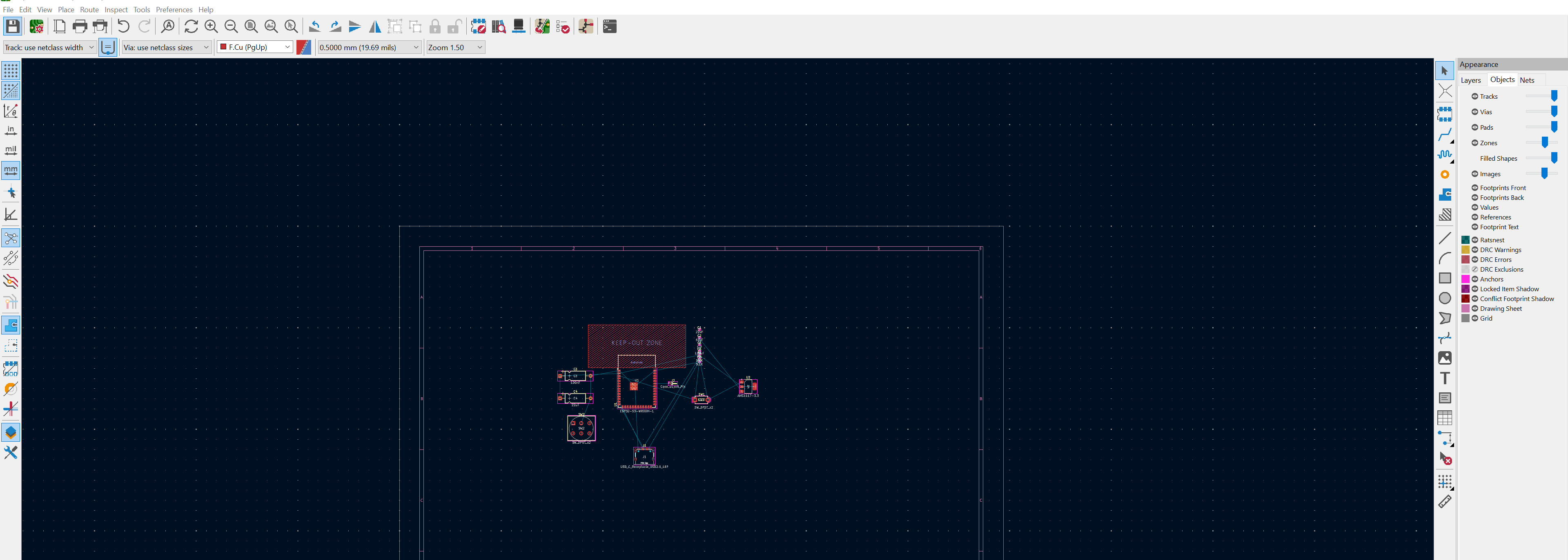
The components where then imported and this is how the appeared.
UNDERSTANDING LAYERS IN KICAD
On the right hand side, there are layers visible in the design. Layers are crucial to the design and manufacturing of a PCB. They define how different aspects of the PCB are organised and visually represented. Layers help with everything from signal routing to creating the physical characteristics of the boards.
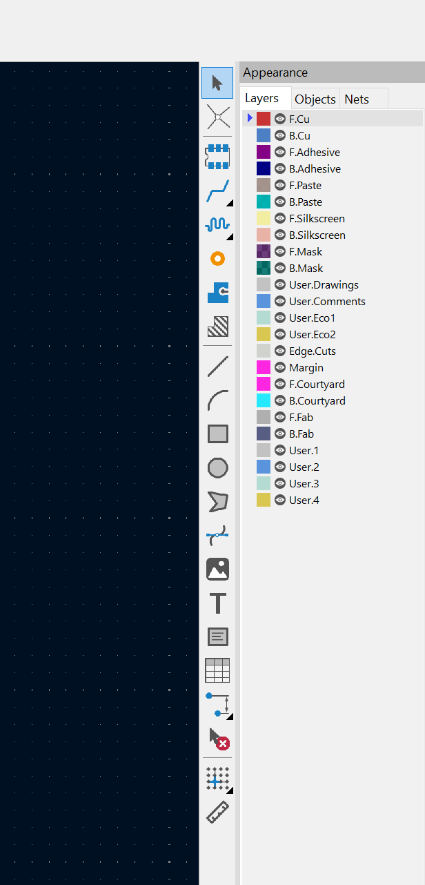
- F.Cu(Front Copper): The top layer where components and traces are placed.
- B.Cu(Back Copper): The bottom layer for routing additional traces.
- Edge.Cuts: Defines the physical outline of the PCB.
- Silkscreen Layers(F.Silks/B.Silks): Used for component labels and markings.
- Solder Mask Layers(F.Mask/ B.Mask): Defines areas that will not be covered by solder mask.
4. ARRANGING COMPONENTS AND ROUTING TRACES
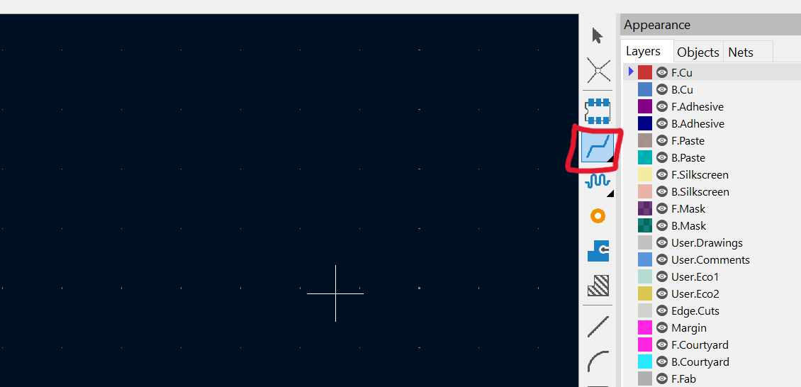
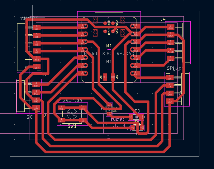
I then arranged the the components in the PCB editor which determoned how my PCB will look. I then used Route Tracks tool(circled in the picture) to make the components connections.
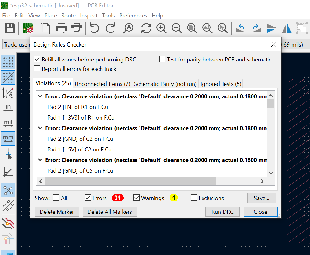
After arranging and making connection lines, I then ran an inspection, using the Design Rule Check (DRC) to see if I properly arranged the components, which I got a lot of errors, so I had to re-do the step.
RE-ARRANGING COMPONENTS
I then re-arranged the components and then re-routed my PCB.
The final routing is as follows,
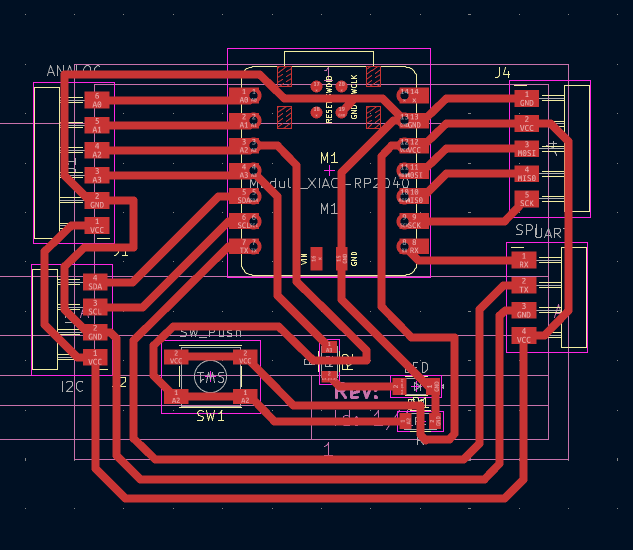
After routing I then added the edge cut layer to give my PCB shape.
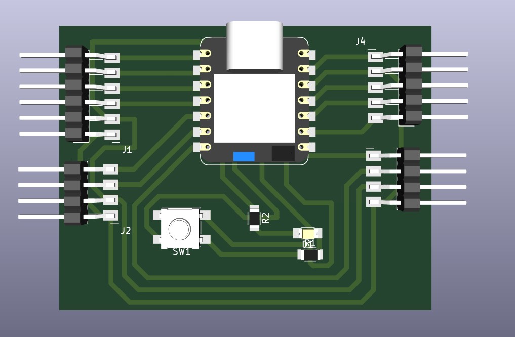
Then to view the 3D model of the PCB I have made i clicked on the grey icon (Circled) which is the
3D viewer.

A 3D view of the PCB to visualize how it will look is as follows:
FILES
The files I have made using the above softwares can be downloaded below.
