Week 08 Electronics Production
Starting to manufacture PCB's
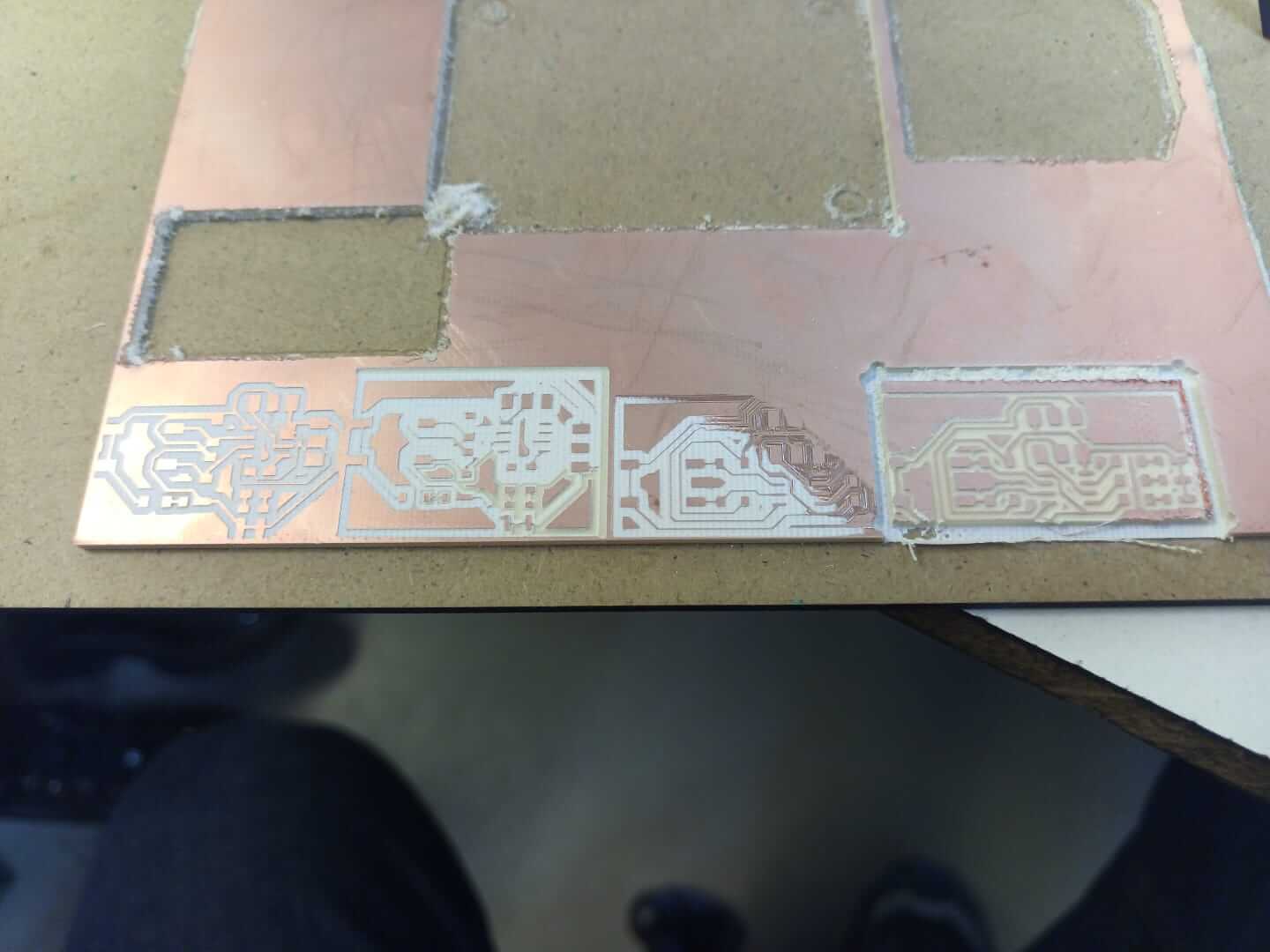
Failed PCB
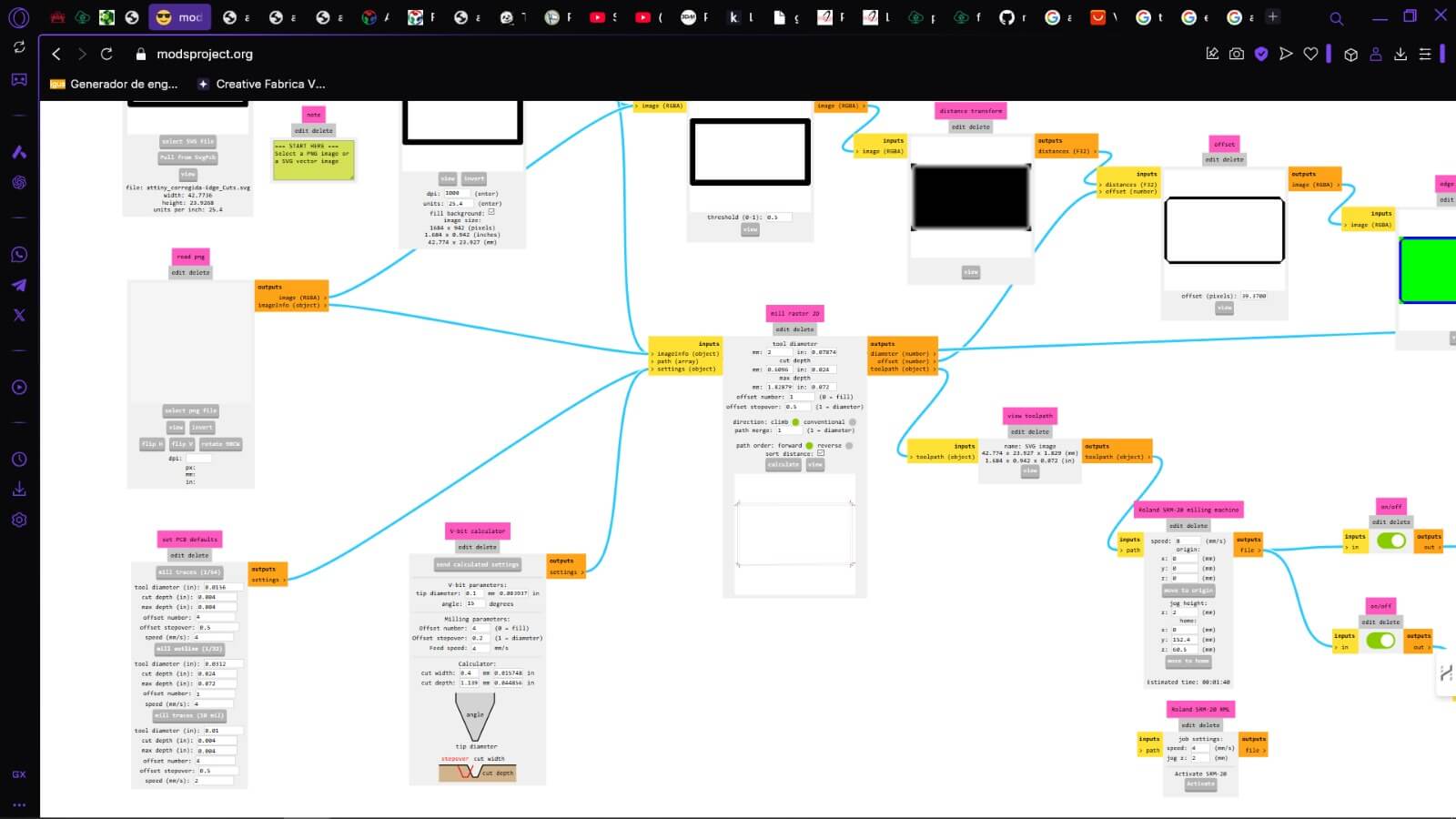
This week's images are purely examples to follow the process, as the numerical values are not clearly visible in the images. However, this is not a cause for concern—the values used in the process are provided within the explanation.
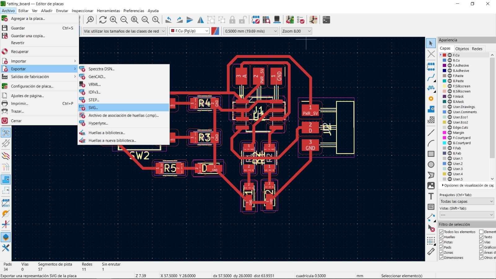
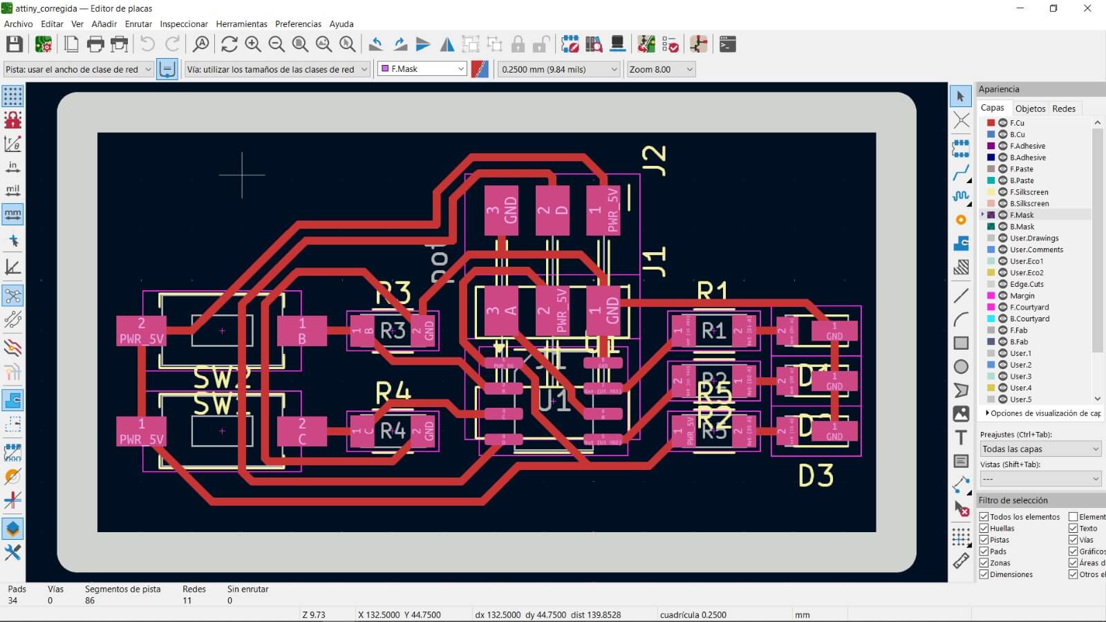
For this week, the circuit board from week 6 was physically made. First, I want to clarify that my first board was incorrect, but in that process, I show all the steps of how to use the software and machines. The correct board will be shown after that. That being said, these were all the parameters I used for KiCad 8.0:
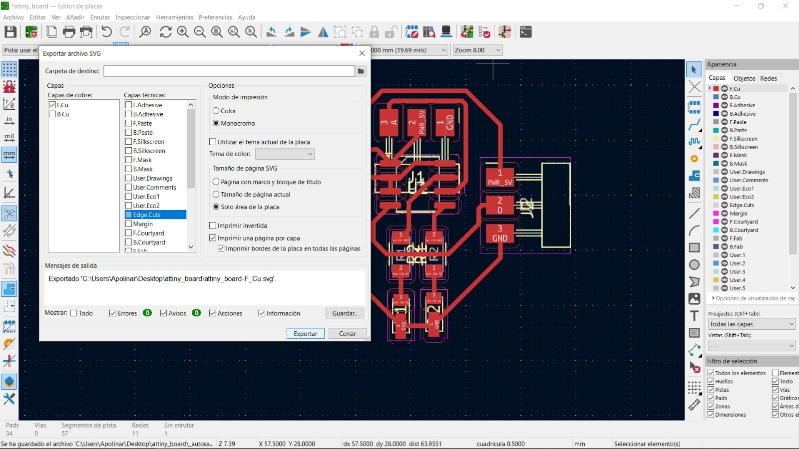
This is how the board looks along with its cutting line, which is located in the 'Edge cuts' layer:
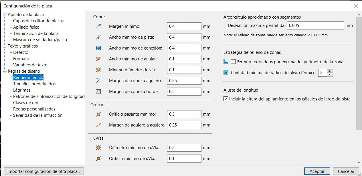
This is the path to export the SVG files used by the CNC software we use, which is called modsproject and is open source:
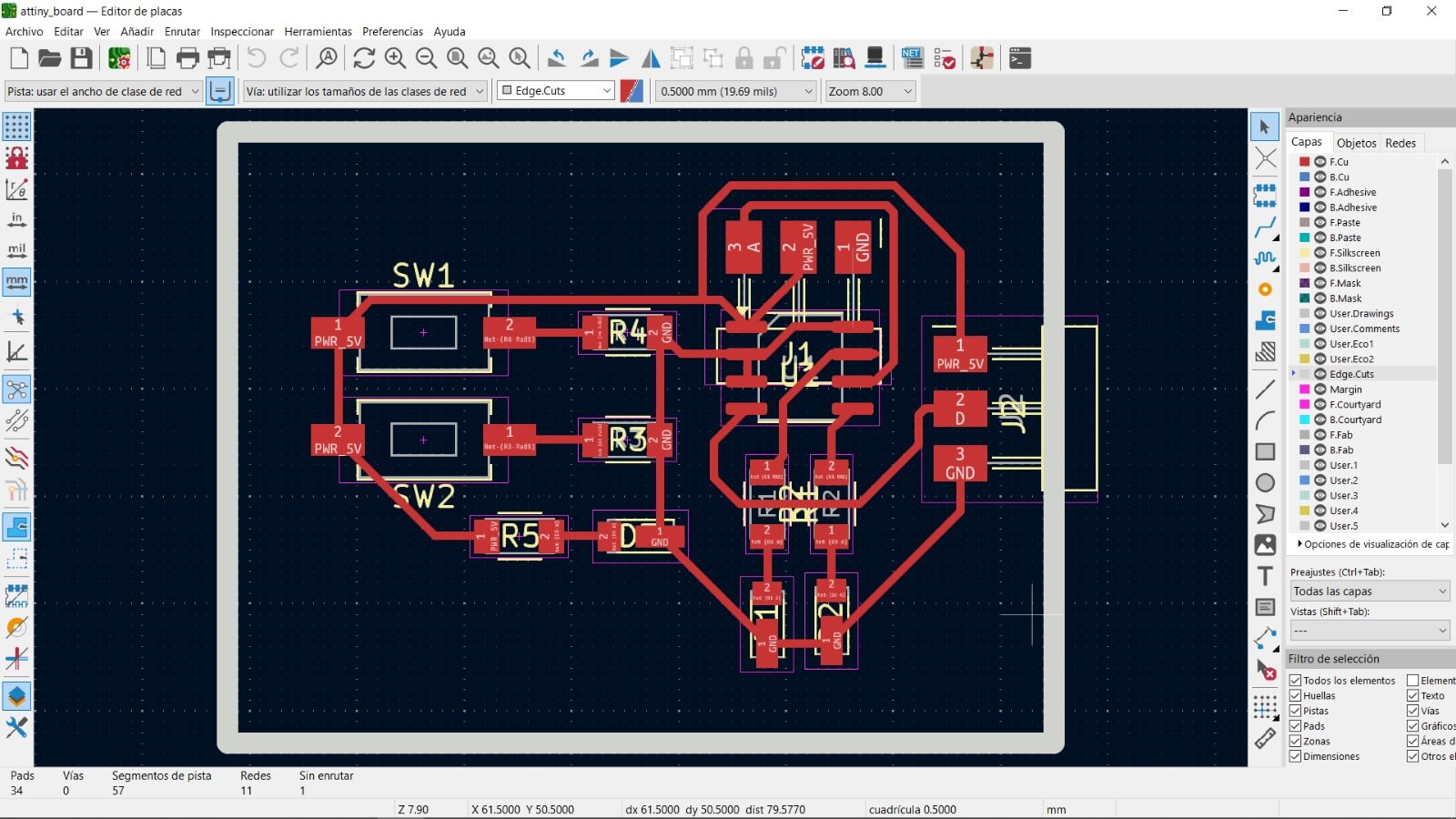
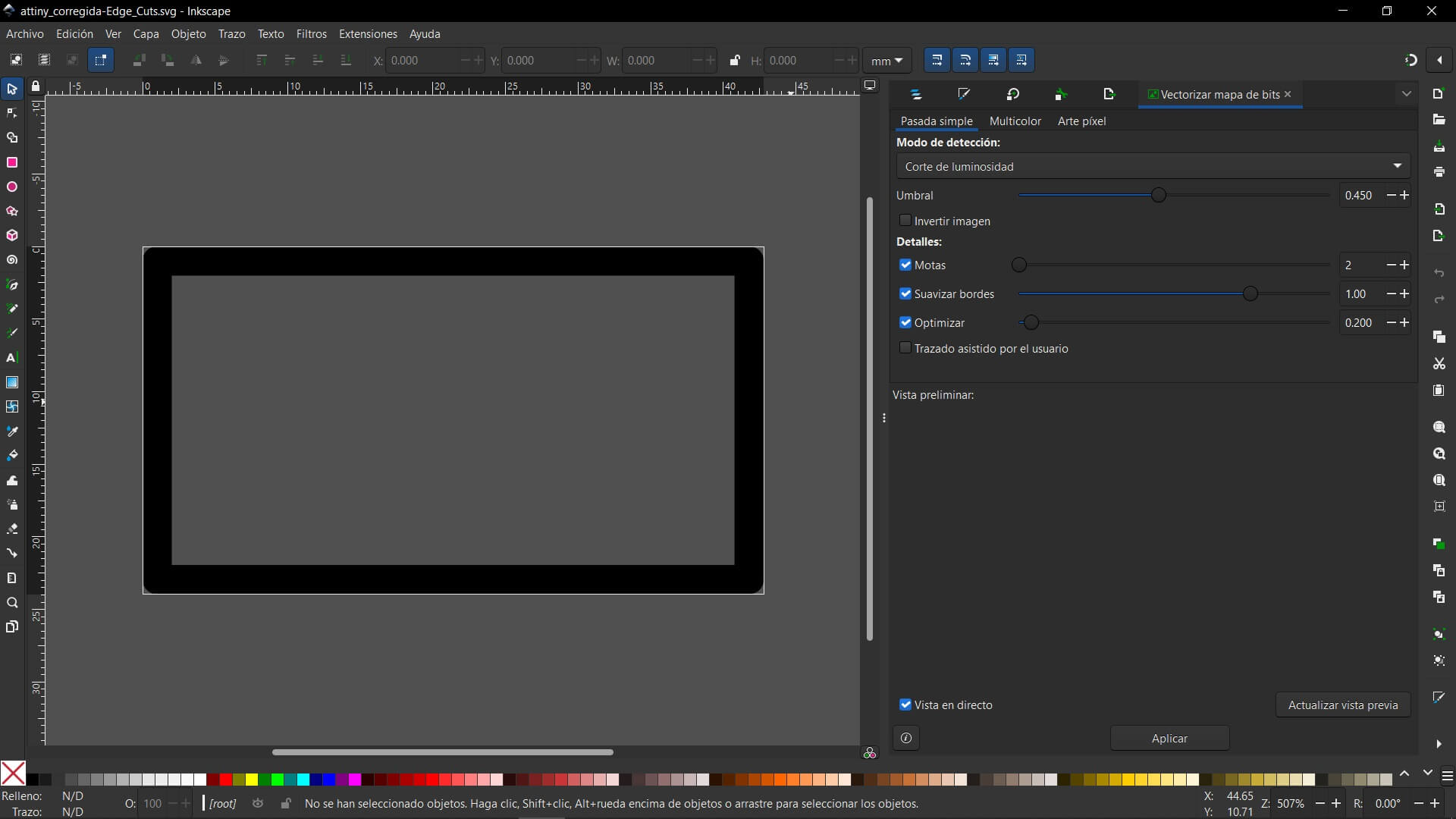
To export only the engraving areas, the rest of the layers must be removed, as shown in the image:
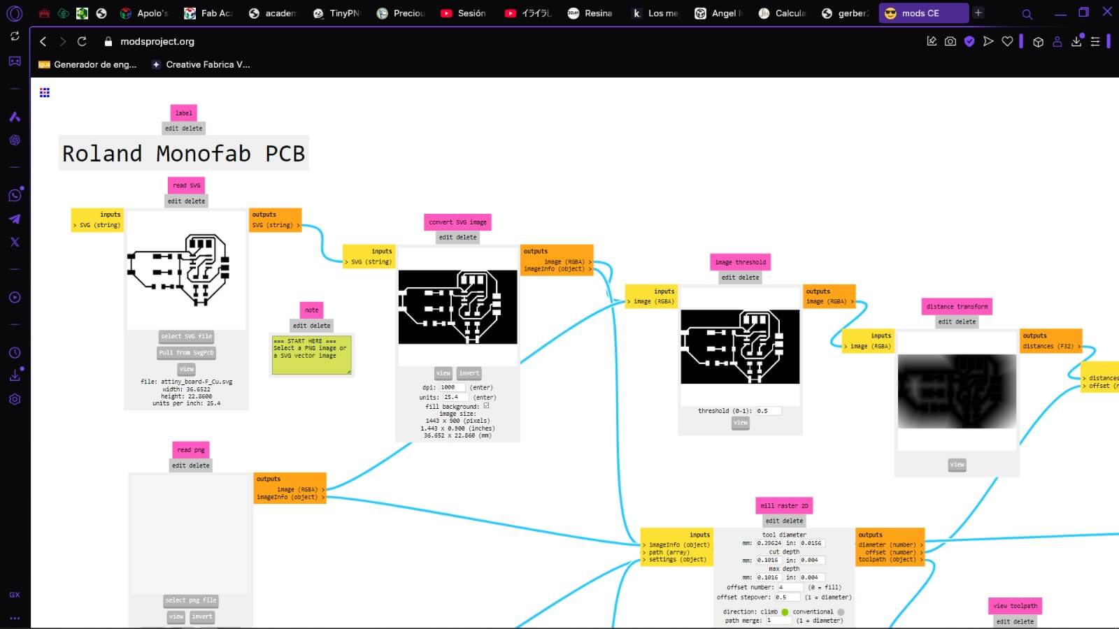
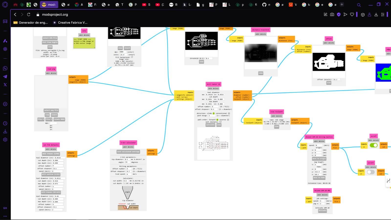
When entering the page, nothing will appear, so we must right-click and, at least for our machine, follow this path: programs > open program > Roland > mill 2D PCB.
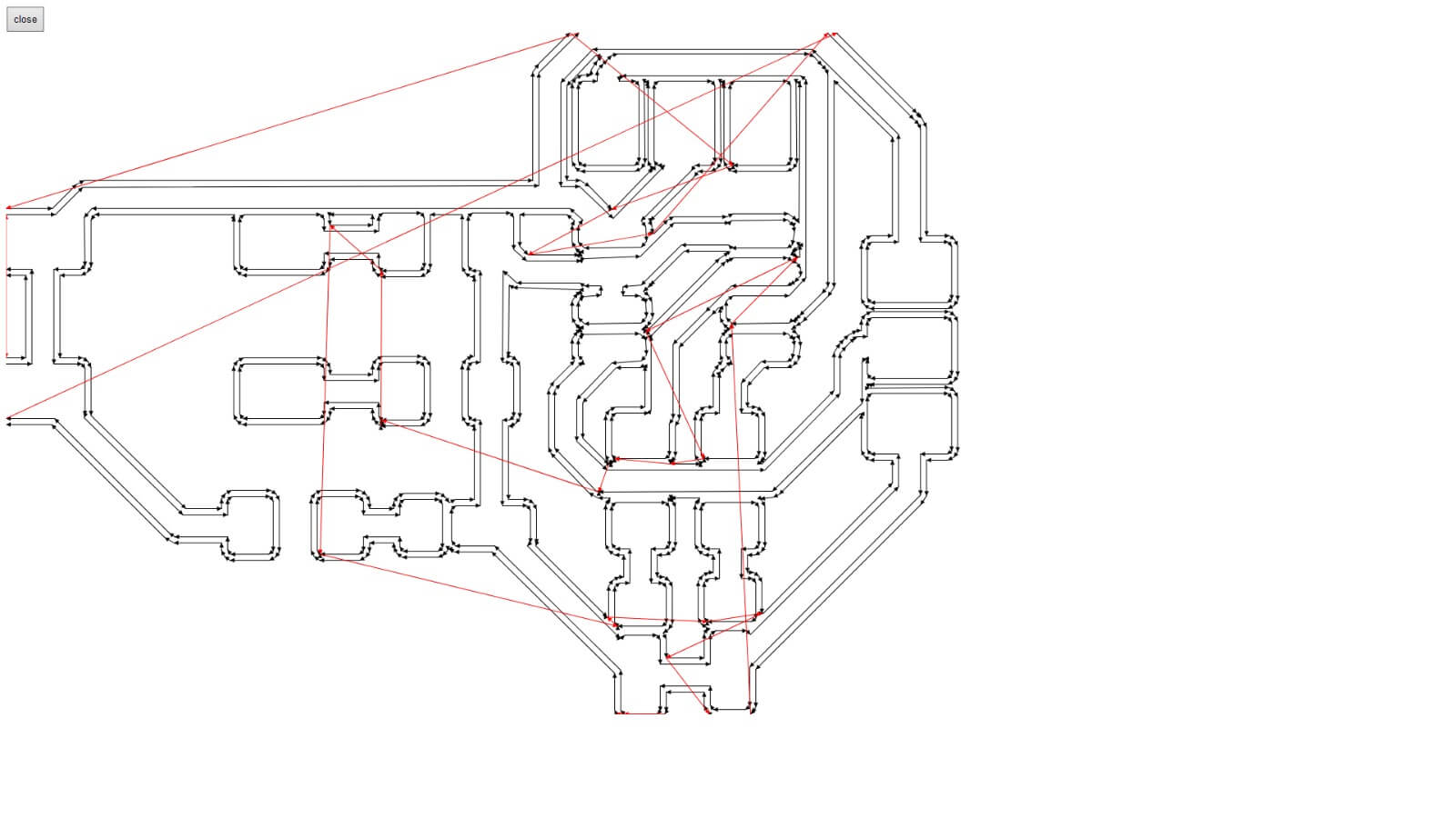
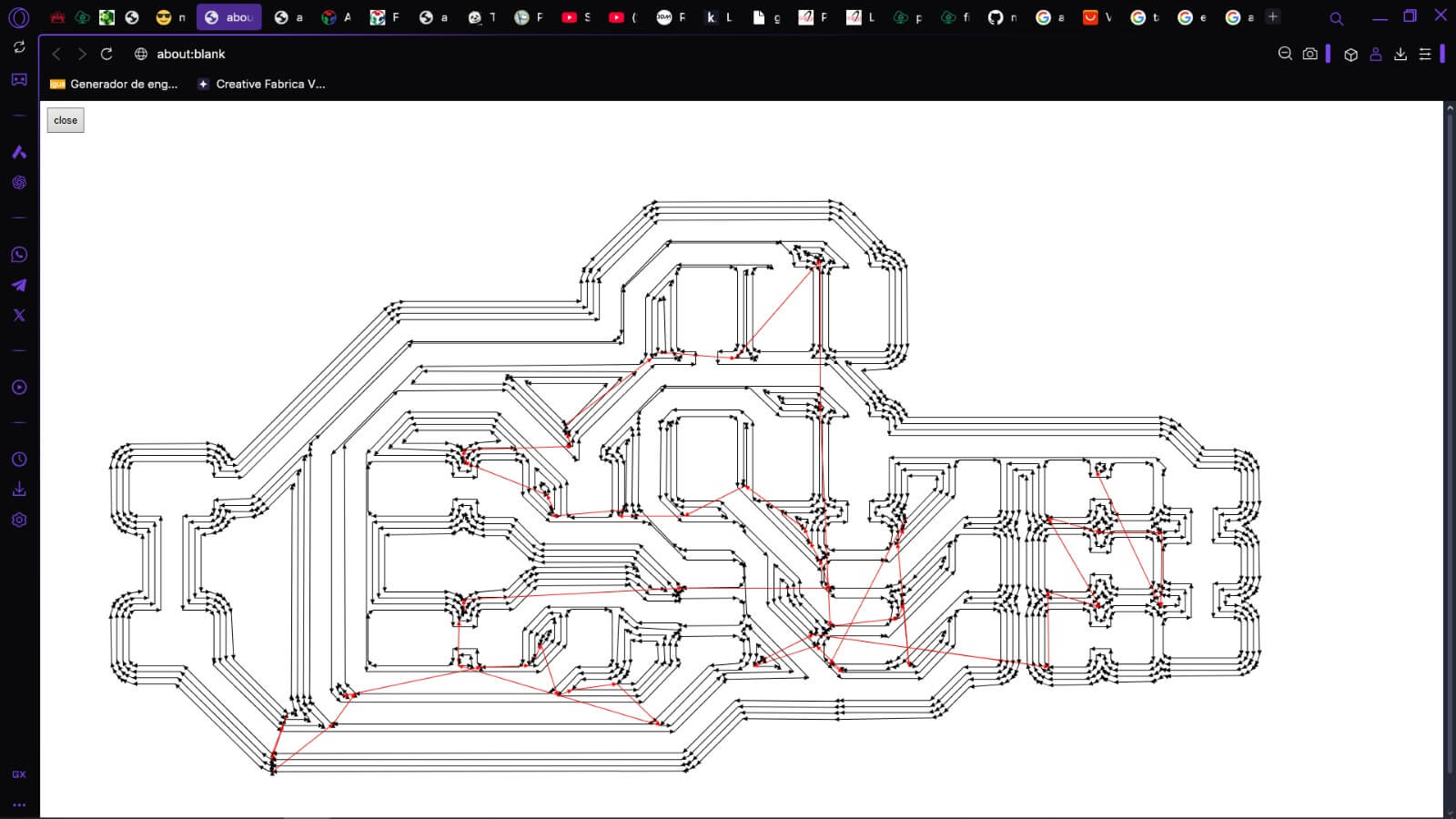
For engraving, the colors must be inverted because the machine 'removes' the black area. For the rest of the specifications, I used all the default settings in the program, first selecting 'mill traces 1/64' to indicate that it will be engraved. (If it's the board's cutting area, 'mill outline 1/12' is selected, and the image colors are not inverted.) Then, I set the axes to 0 and finally pressed 'calculate' to show how the route would be made and to download the file that will be sent to the CNC.
The boards are secured with several lines of double-sided tape to a sacrificial bed, which is screwed in at four points to a custom-made bed built in the lab specifically for the machine. On the other hand, even though the online program specifies tool measurements for 1/32” or 1/64” diameter tools, we do not use any of those. We replaced the 1/32” tool with a V-bit, which is thinner than 0.4 mm, but it works quite well for us. Also, when using drilling tools, we change the tool diameter to 0.8 mm, and for outer cutting, we change it to 2 mm.
The movement speeds I use are: for the engraving tool, 4 mm/s; for the cutting tool, 8 mm/s; and for the drilling tool, 0.5 mm/s (this is because the tool has a 0.8 mm diameter and is easy to break—there have been cases where exceeding those limits caused it to break).
It is worth noting that the bed has never come loose using our current method of securing it and the speeds I've mentioned.
It is important to note that the CNC software will not open unless the machine is connected.
The first step is to set the axes to 0, making sure the corresponding tool is already placed in the machine.
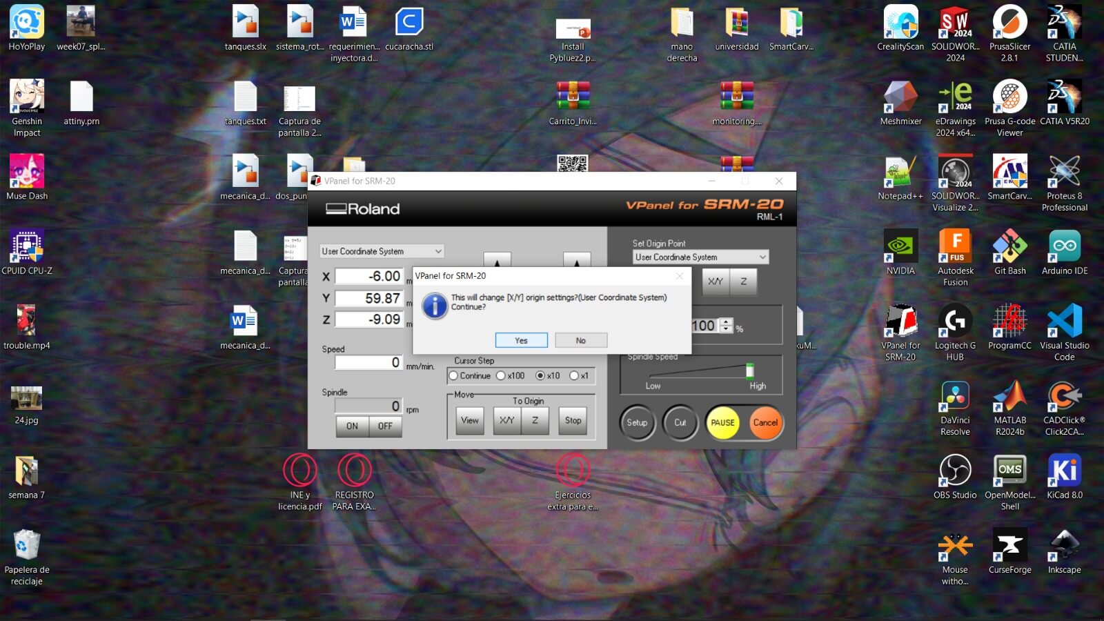
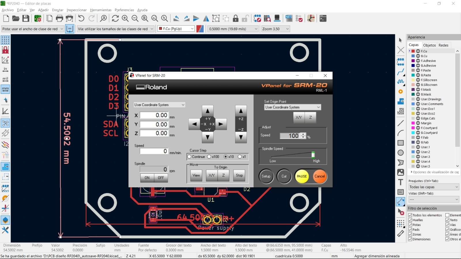
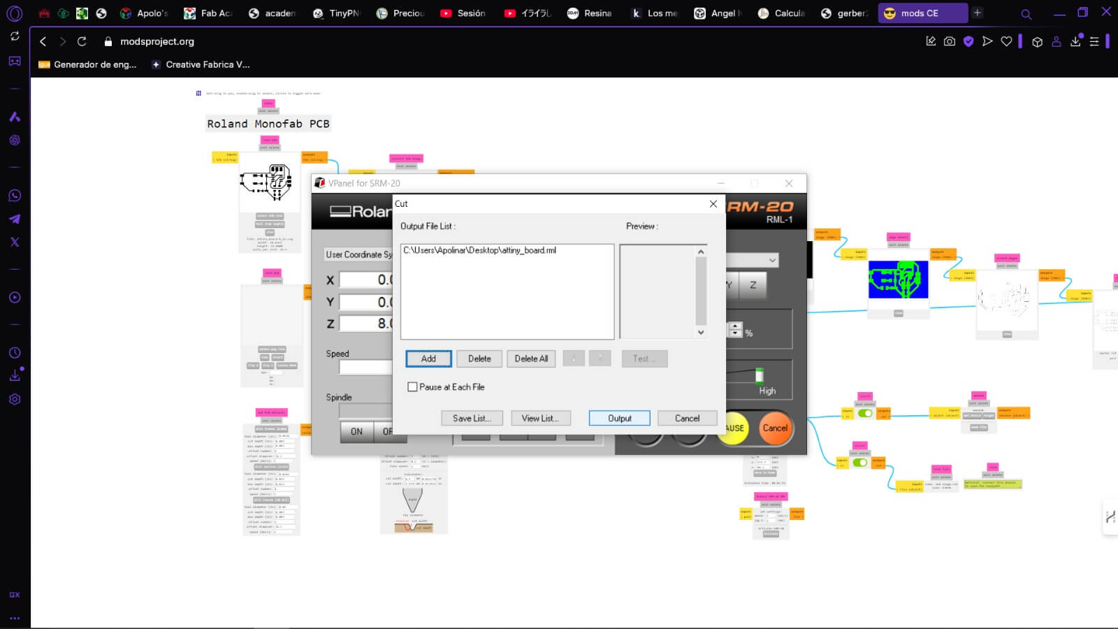
Then, the program is loaded, and the machine does the rest, but we have to change the tool and set the 0 of the axis.
Regarding the rotation speed of the tool, at least to my knowledge, it is not possible to modify it, and therefore the website where I do everything does not mention it either. However, the control software shows us that when the spindle is turned on, the tool spins at 8000 rpm for all the mills.
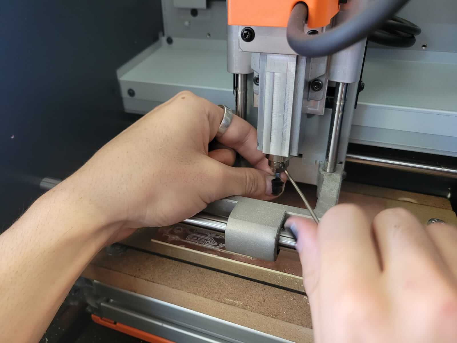
The way to set the zero for the Z-axis, at least in my case and the method I prefer, is to bring the Z-axis with the tool installed as close as possible without touching the phenolic board. Then, I loosen the tool from the spindle, let it drop until it touches the board, and then, from the machine's software, while the spindle is running to prevent the tool from chipping or breaking, I lower the Z-axis by 0.05 mm.
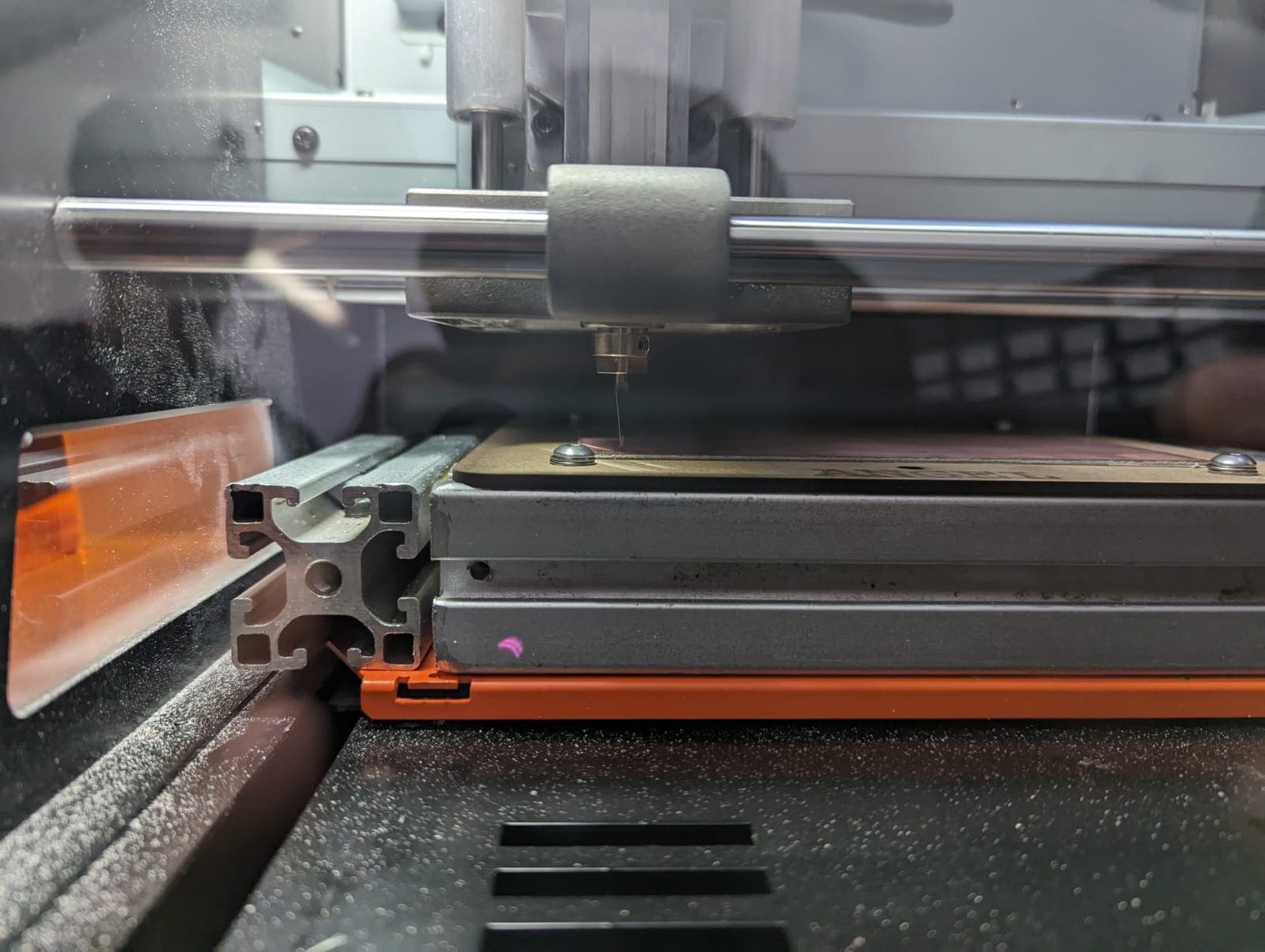
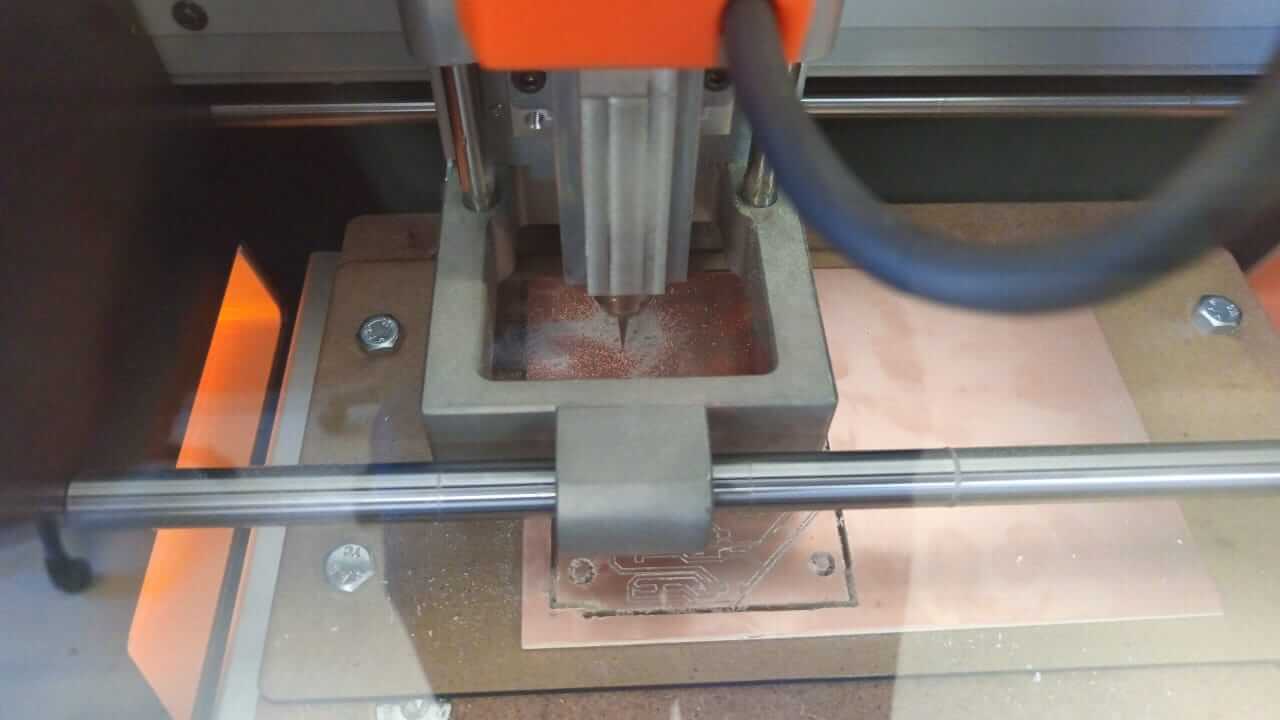
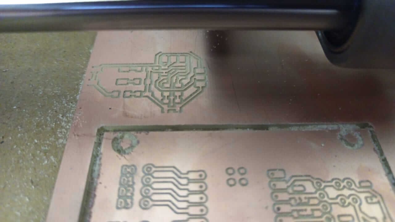
Once that is done, the components are soldered onto the board.
For this, the method I use to solder SMD components: First of all, it's worth mentioning that I use the soldering iron at 380–400 °C, since I tend to solder a bit quickly. I apply solder paste on the pads, heat them up, and add a small amount of solder. Then I apply paste to the component, solder only one end of the component, and if it aligns correctly with the pads, I can freely solder the other side.
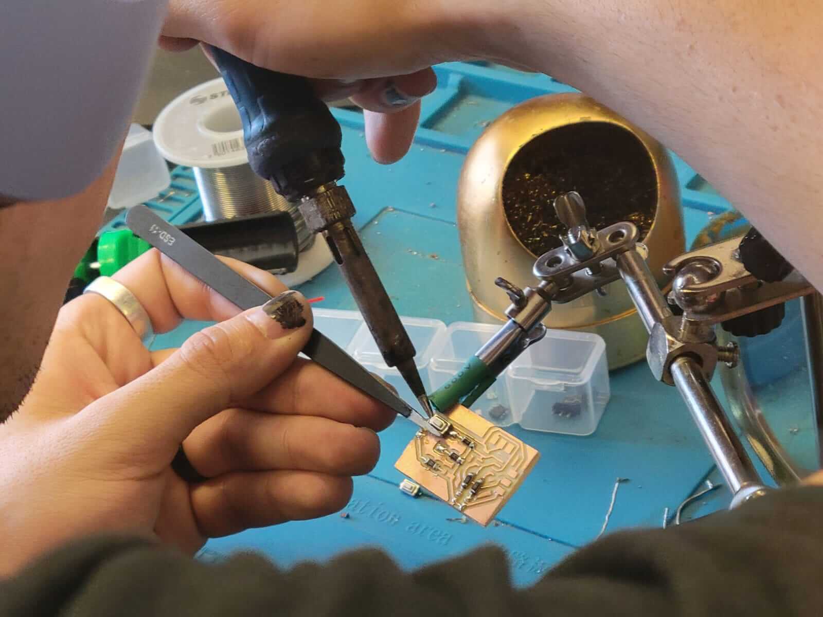
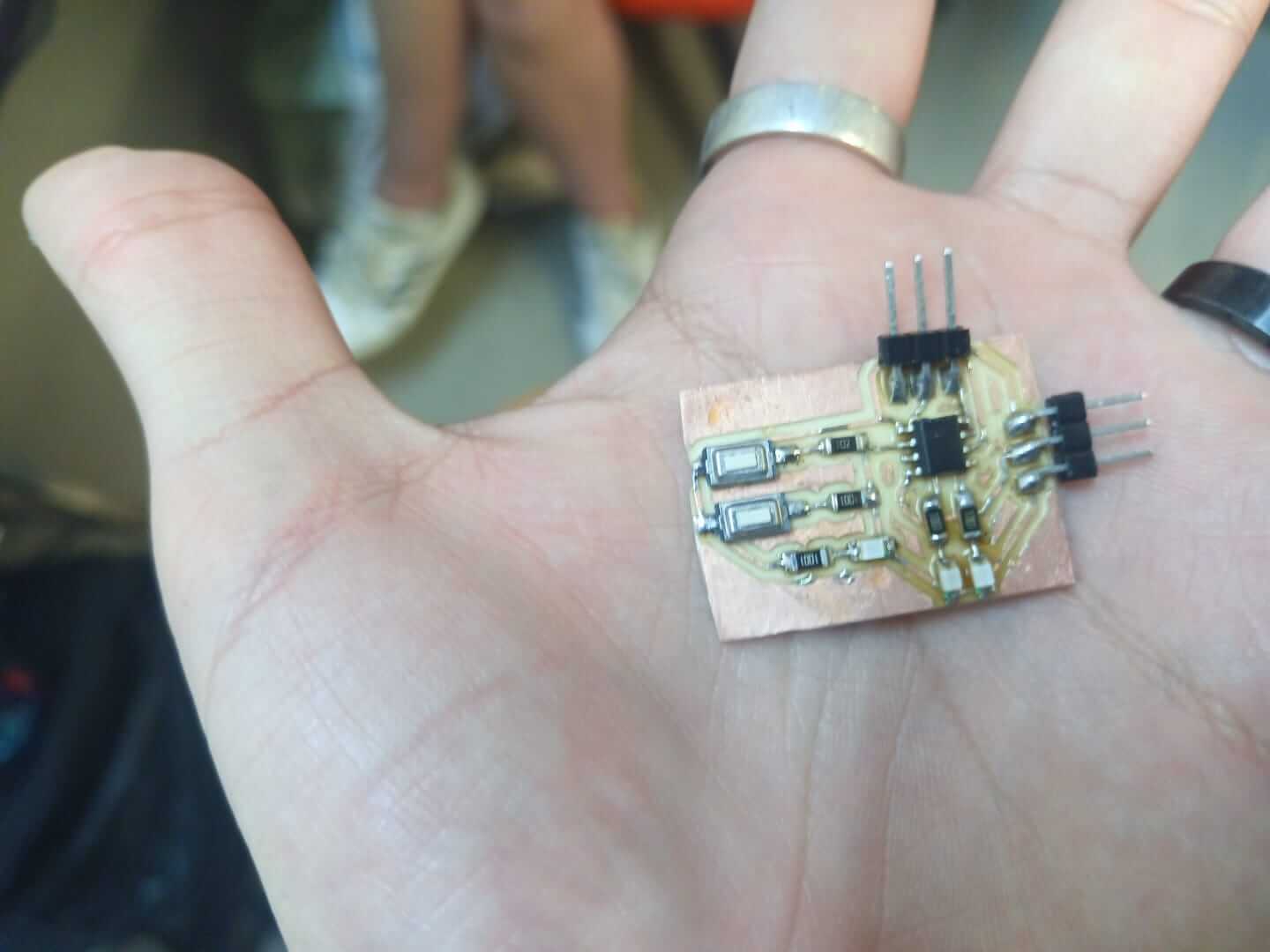
After this, the board is programmed, but as I mentioned at the beginning, the first board was not made correctly, so it is not worth showing failed codes.
True PCB
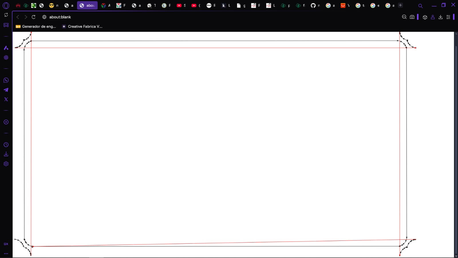
This is how my SVG files looks like:
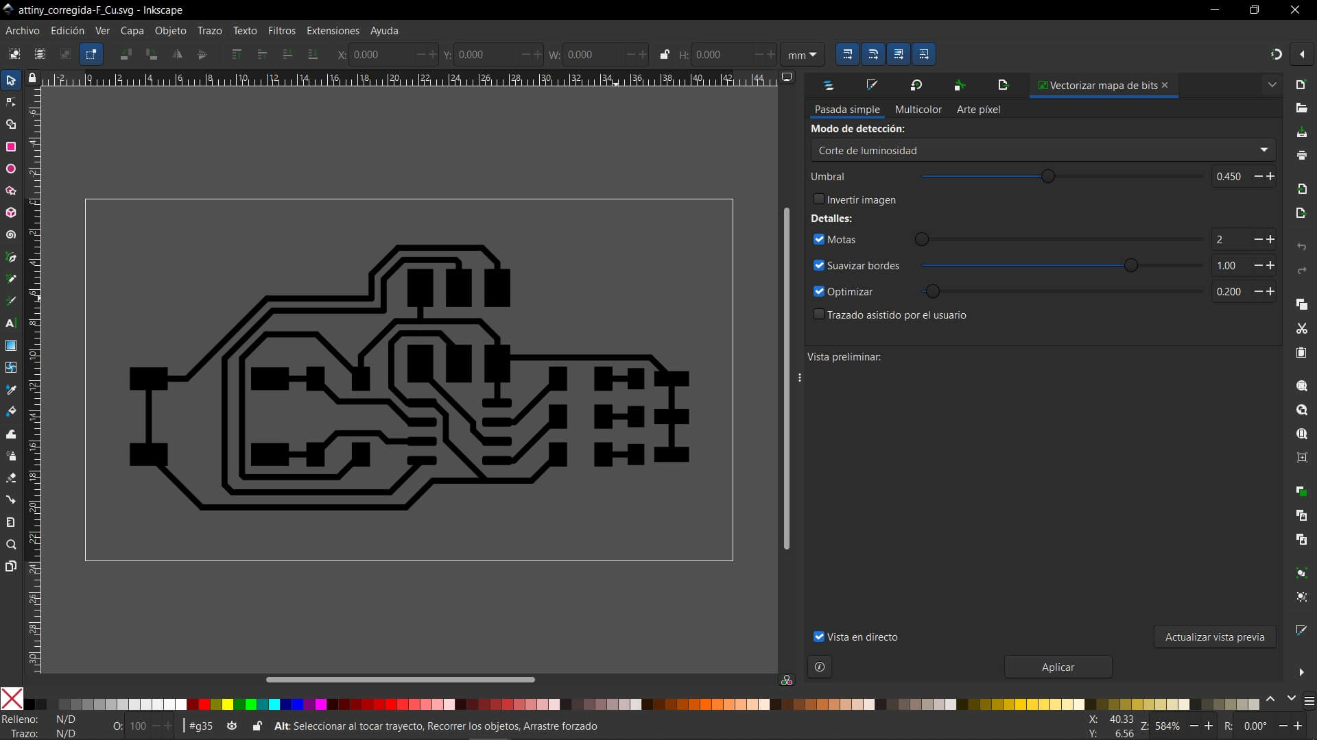
Now, here is a quick summary of the second board:
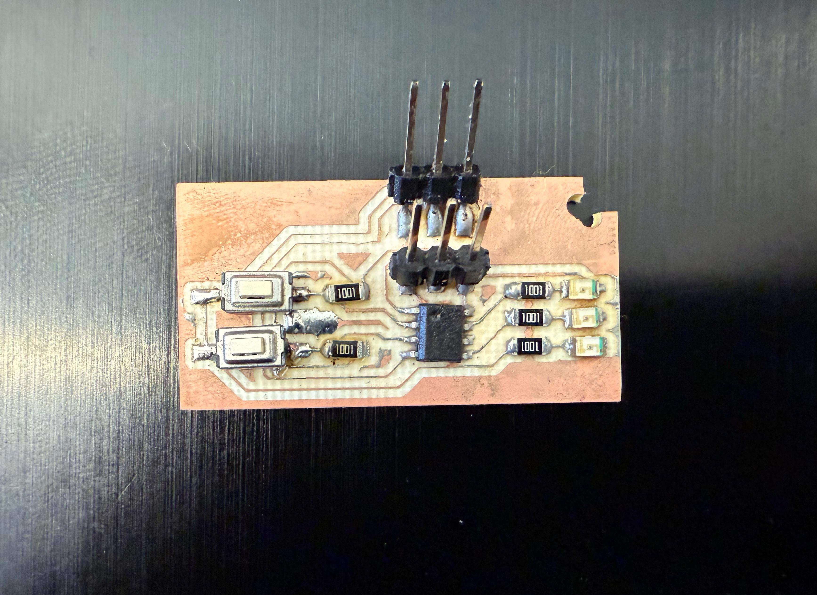
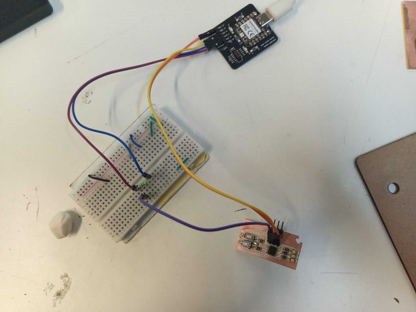
To program this Attiny412, I used a development board made at the Fablab called Quentorres. Here is the link so you can see the full process.
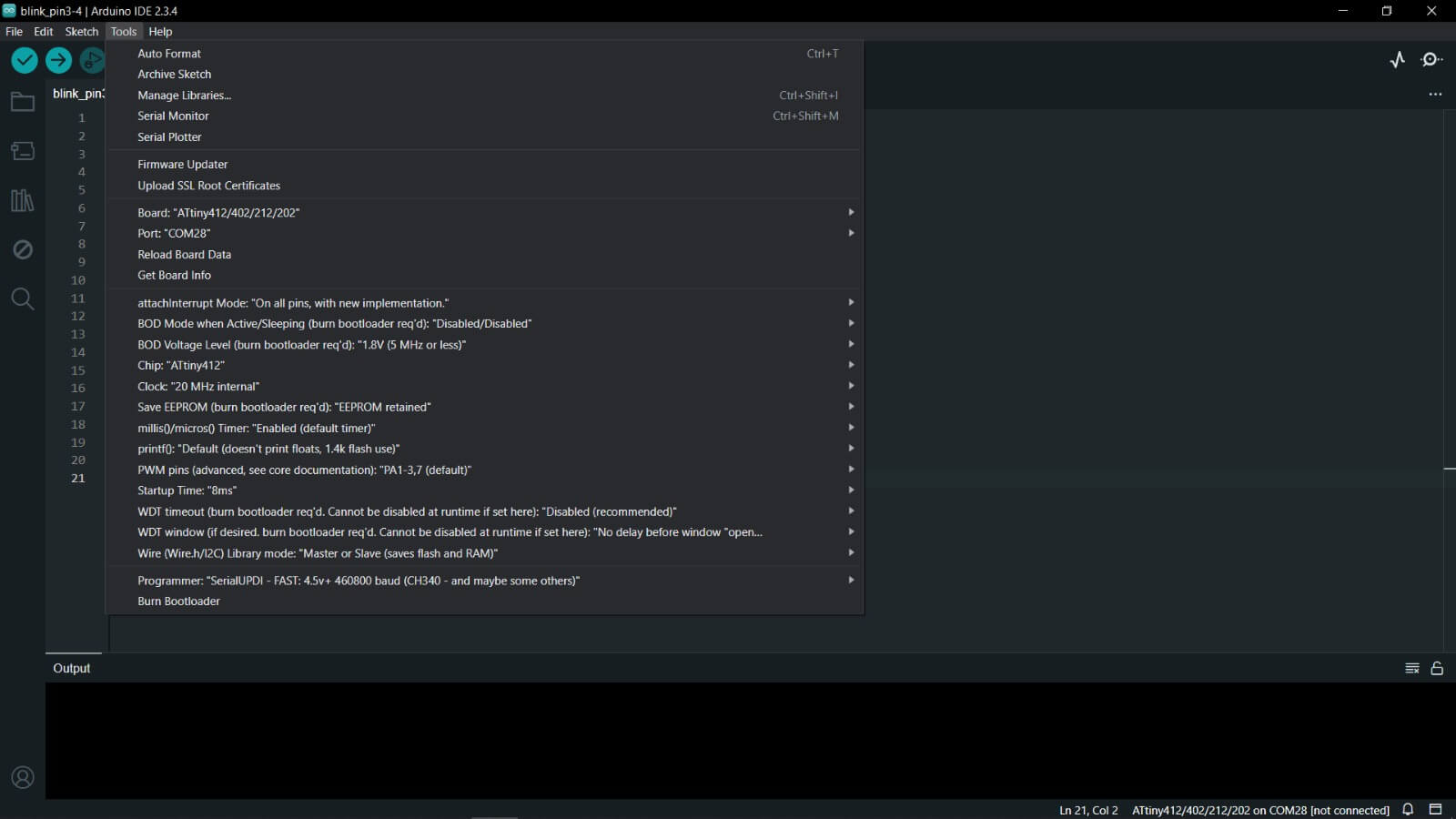
However, it is important to clarify that to program it, new board definitions must be installed in the Arduino IDE, and a resistor must be placed in parallel with RX and TX for proper programming.
Once everything is installed correctly according to the tutorial in the link, the parameters should be set as follows:
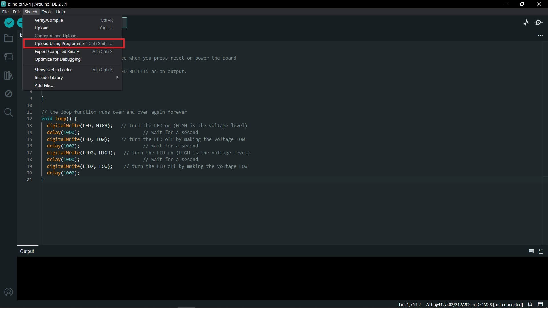
And it is uploaded using this button:
This is how it's connected my PCB:
I used this two codes to demostrate that my board works
//blink
int LED = 4;
int LED2 = 3;
void setup() {
    pinMode(LED, OUTPUT);
    pinMode(LED2, OUTPUT);

}

void loop() {
    digitalWrite(LED, HIGH);
    delay(1000);
    digitalWrite(LED, LOW);
    delay(1000);
    digitalWrite(LED2, HIGH);
    delay(1000);
    digitalWrite(LED2, LOW);
    delay(1000);
}
//button
const int led1 = 3;
const int led2 = 4;
const int boton1 = 0;
const int boton2 = 1;

void setup() {
    pinMode(led1, OUTPUT);
    pinMode(led2, OUTPUT);
    pinMode(boton1, INPUT_PULLUP);
    pinMode(boton2, INPUT_PULLUP);
}
void loop() {
    if (digitalRead(boton1) == LOW) {
    digitalWrite(led1, HIGH);
    } else {
    digitalWrite(led1, LOW);
    }

    if (digitalRead(boton2) == LOW) {
    digitalWrite(led2, HIGH);
    } else {
    digitalWrite(led2, LOW);
    }
}
This week, I had several problems. First, since I am not very skilled in KiCad, I struggled a lot with exporting things to the online program. Second, most of my boards came out fine, but they were ruined by the outer cut of the board. I ended up solving this by shifting the axes slightly down and to the left. The biggest problem I had was a "small" typing error, where the buttons were not correctly placed in KiCad itself. So, I basically had to redo the entire board. But in the end, everything was successfully completed.
Here you have the link to our group page
Here you can find the files of each process:
