Week 06 Electronics design
Starting to design the first electronic boards
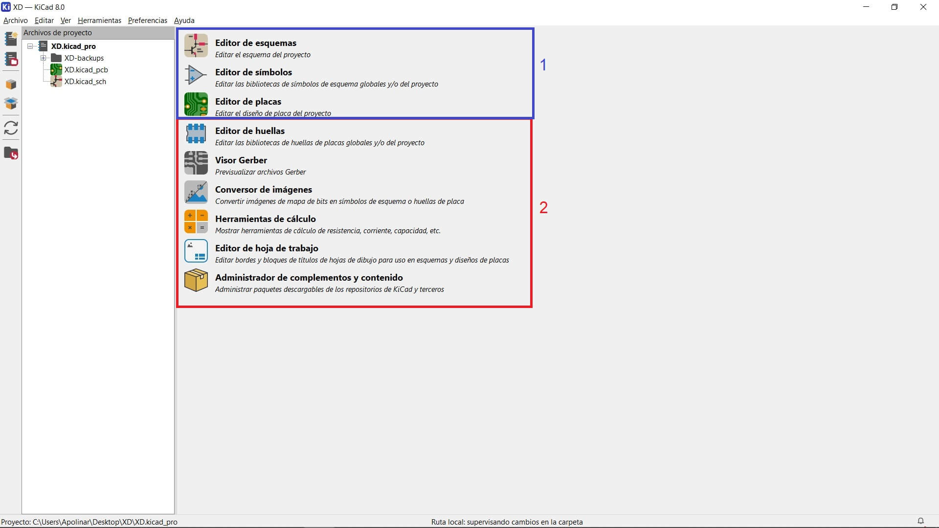
What we were taught in class was basically how to create a PCB in KiCad 8.0 using the first three tools shown in the image, as well as the most basic tools within the interface, such as the different calculators, managers, and other tools available in the program, which are marked in red.
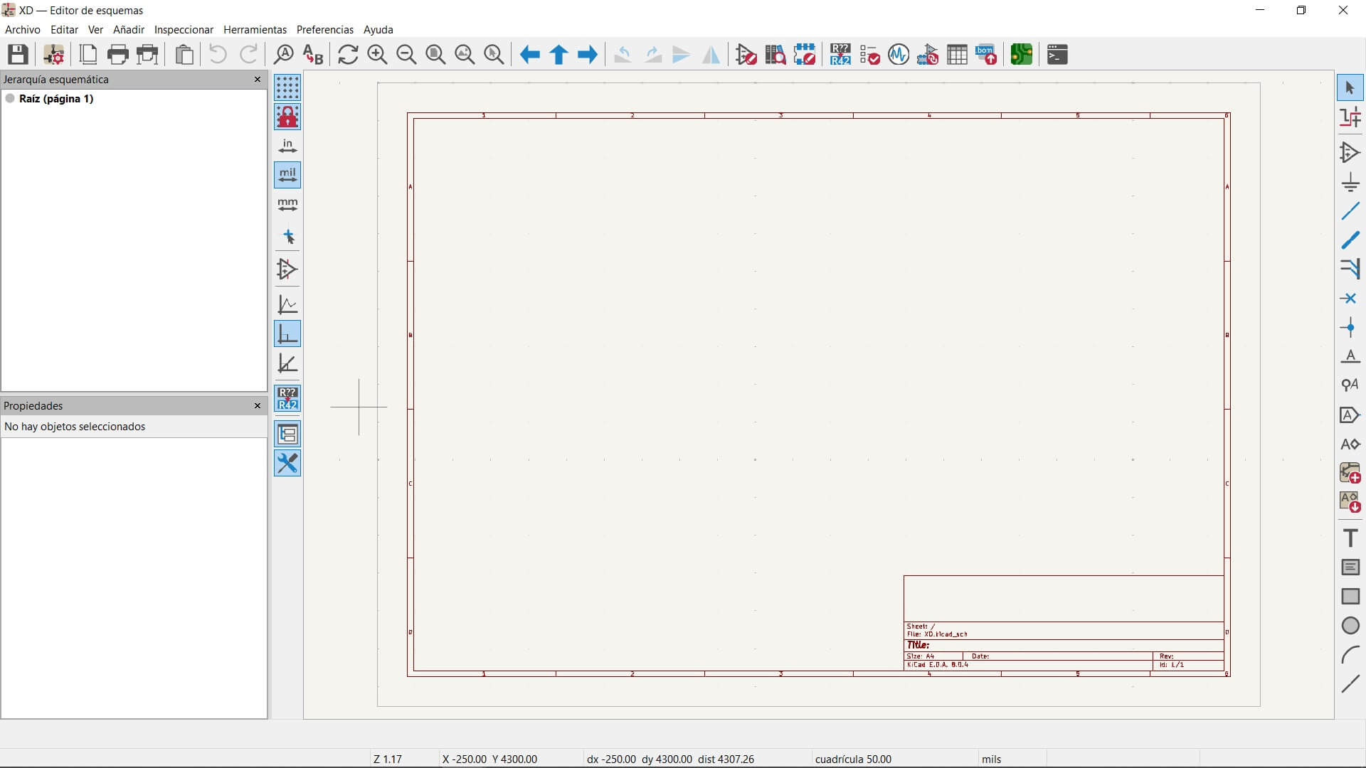
The schematic editor works quite similarly to any other; there is no mystery to it, and this is what it looks like.
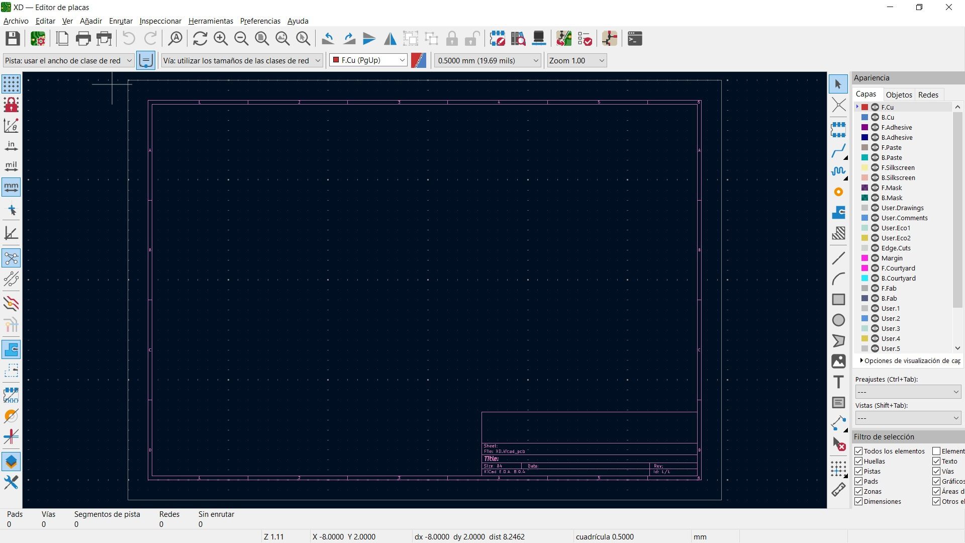
The same applies to the PCB editor. I must say that I was expecting a more complex interface, since it is used for designing electronic boards, but fortunately, that was not the case, as this was the only tool I needed to use.
If you want to add a new library to the program, first download and extract the chosen library to your preferred directory. To add it to the program, go to Preferences > Manage Symbol Libraries / Manage Footprint Libraries, as it will be done in both cases
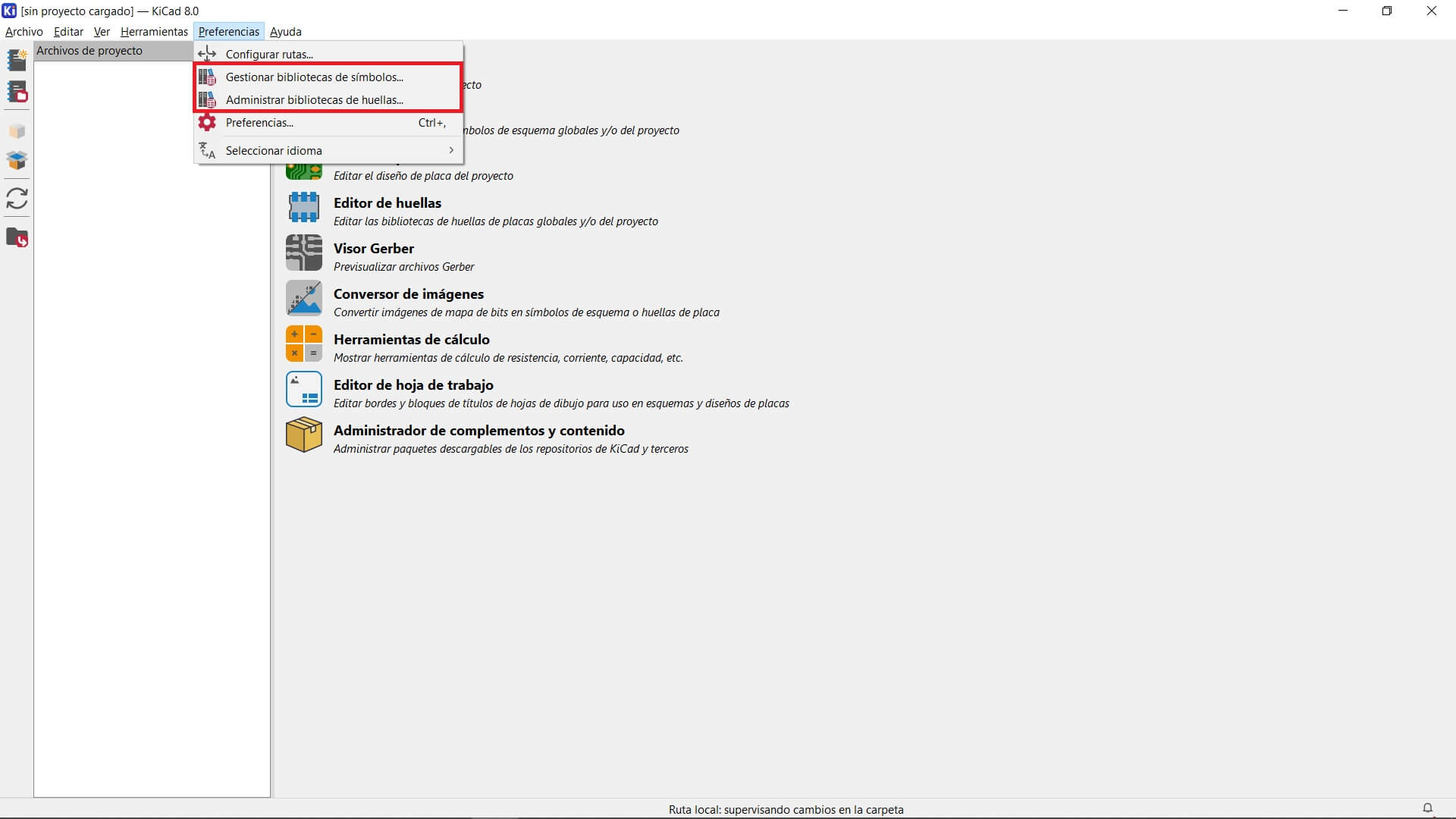
Once inside either option, you need to add a new directory by clicking the "+" button and then assign an appropriate name to the library.
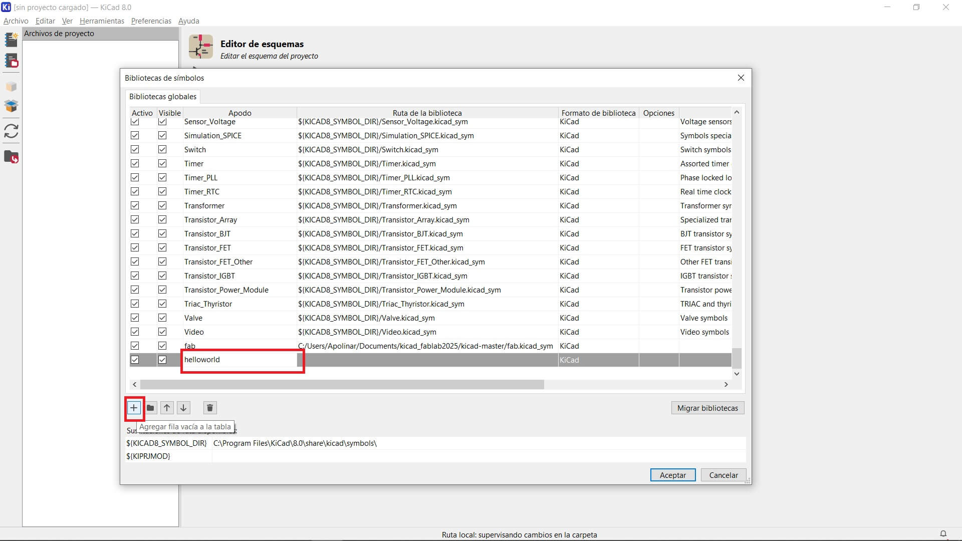
Next, select the directory where the library was extracted and choose the corresponding file, either footprint or symbol. The process is the same in both cases.
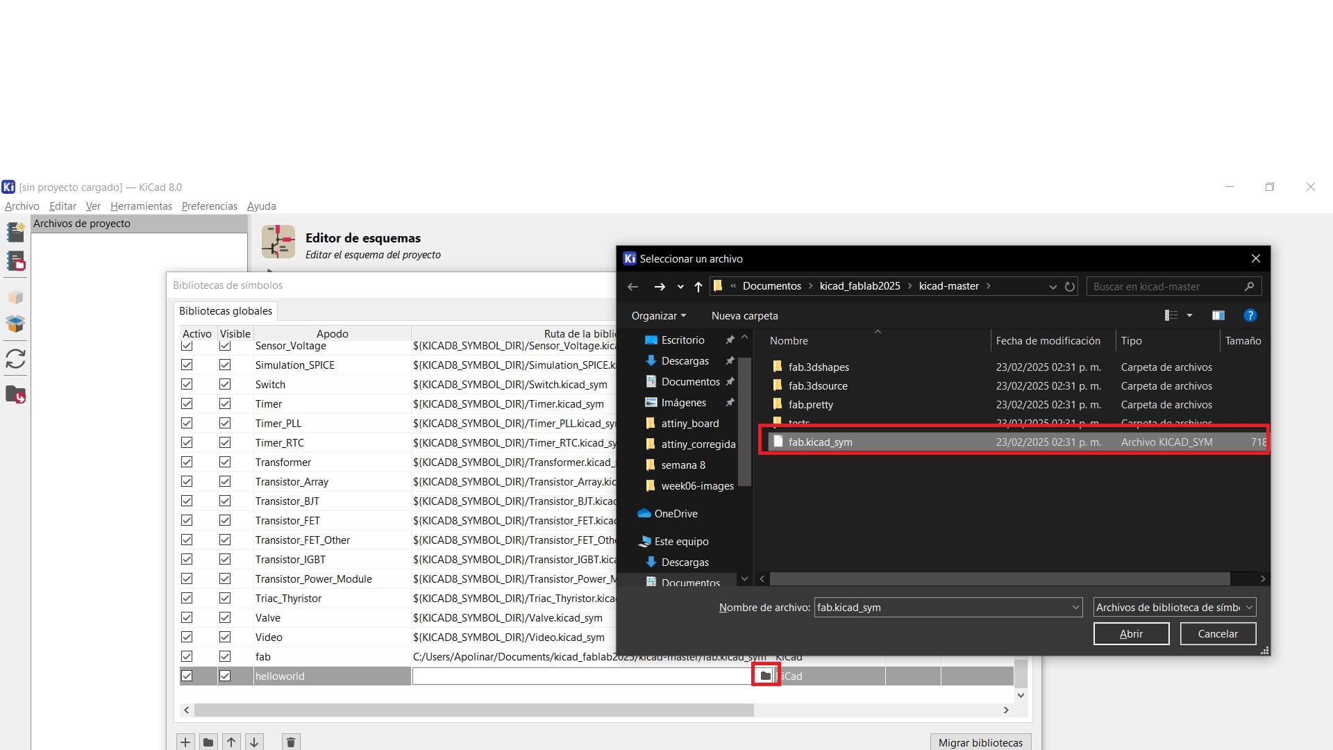
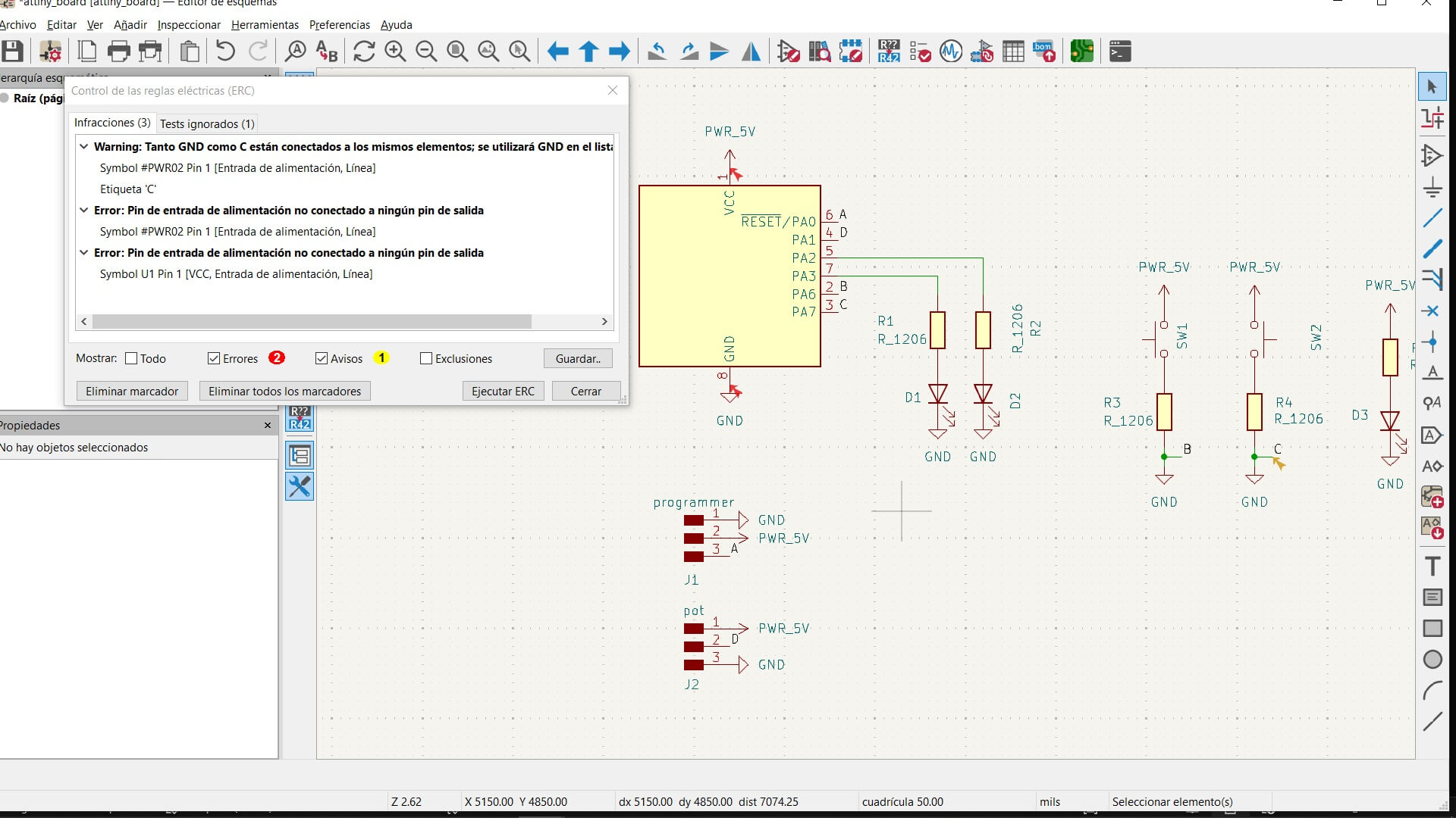
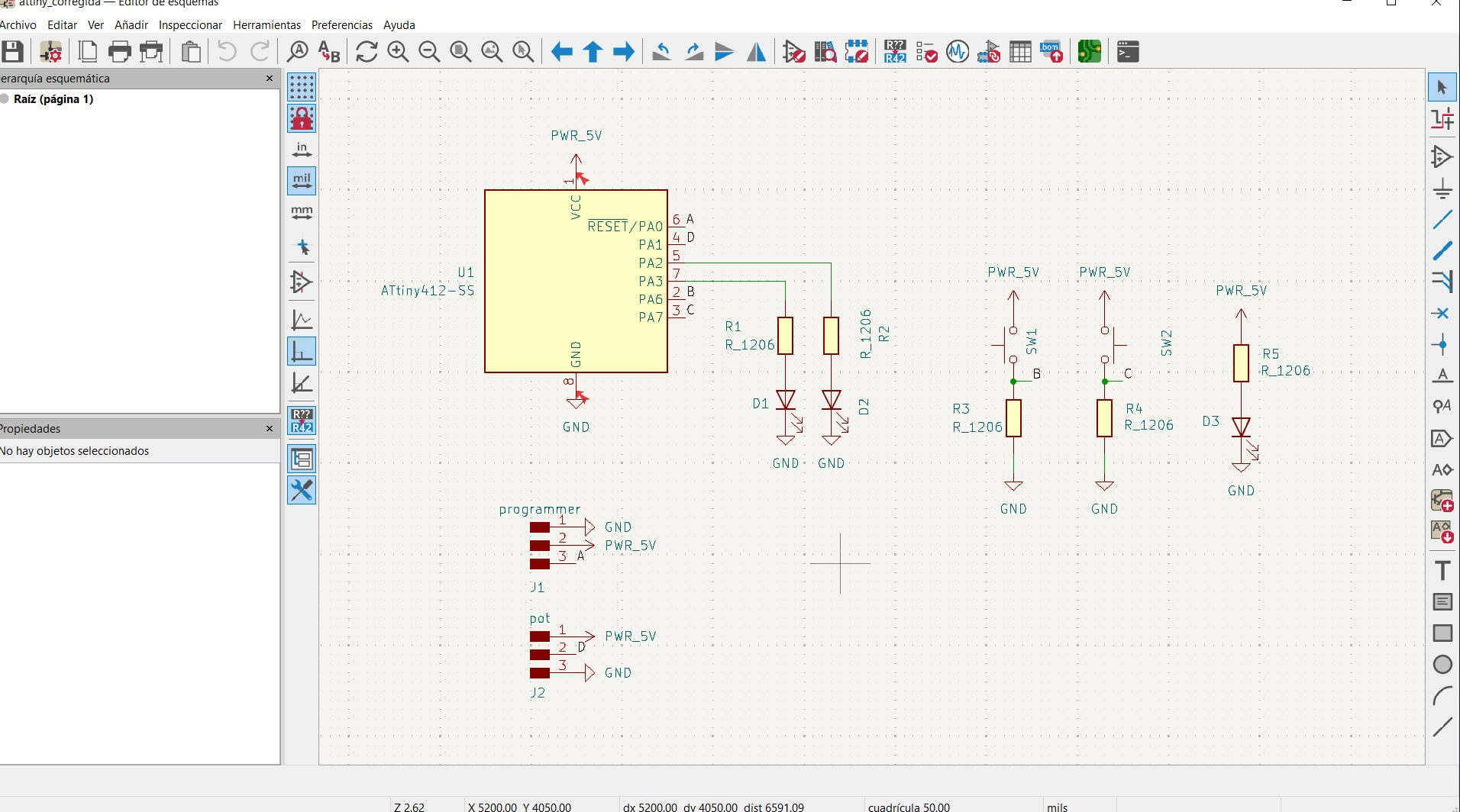
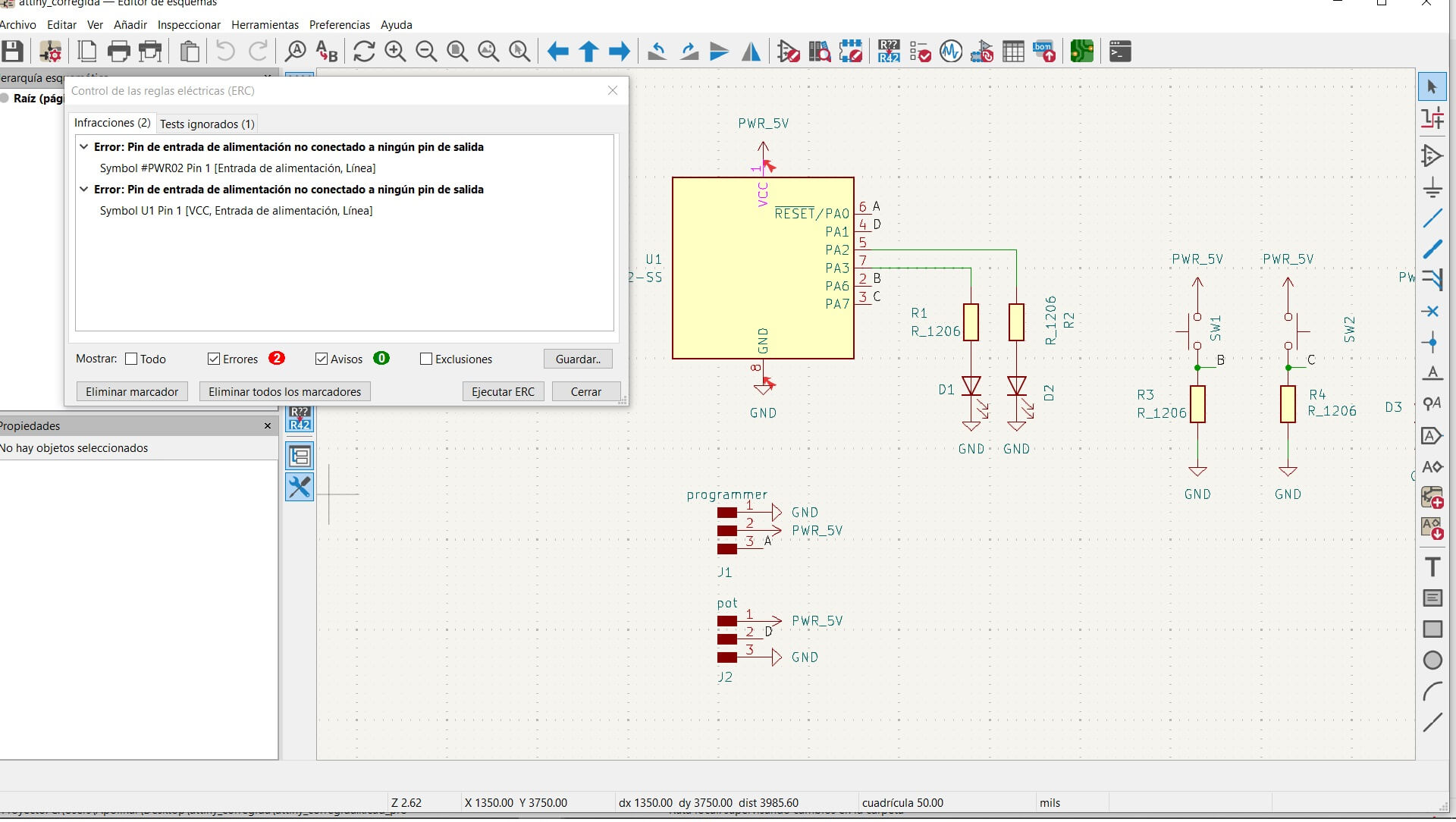
As I mentioned before, I didn't know what to do, so I decided to add simple components to make use of my microcontroller's pins. The only components I added to the microcontroller's pins were two buttons on pins PA6 and PA7 (B and C, respectively) with a pull-down configuration, two LEDs on pins PA2 and PA3, and a potentiometer for PWM (which will be placed externally to the board due to the limited availability of materials in our lab). The PA0 and PA1 pins were not left free, as I mentioned, PA1 (D) is for an external potentiometer (but it can be used for anything else), and PA0 is used to program the Attiny with UPDI. Additionally, I added an LED outside of the pins to ensure that the board receives power, as it will remain lit whenever the board is powered.
Since my LEDs are red, I will consider their higher operating voltage, which is 2.2V, while my supply voltage is 5V. Based on the datasheets, the maximum current a LED can withstand is 60mA. However, I decided to work with 3mA to avoid excessive current consumption. Therefore, the calculated resistance value for my LEDs is:
R = (5 - 2.2) / 0.003 = 933Ω
Since commercial resistors do not have this exact value, I will use the closest one, which is 1kΩ.
Considering that very small resistance values can cause the power rating to be exceeded when the button is pressed, potentially burning out the resistor, it would be a good idea to use higher resistance values. However, using excessively high values can result in a "floating" state. Based on my experience, a good resistance range for buttons is around 1 kΩ, which works well for me since it matches the resistors used for my LEDs.
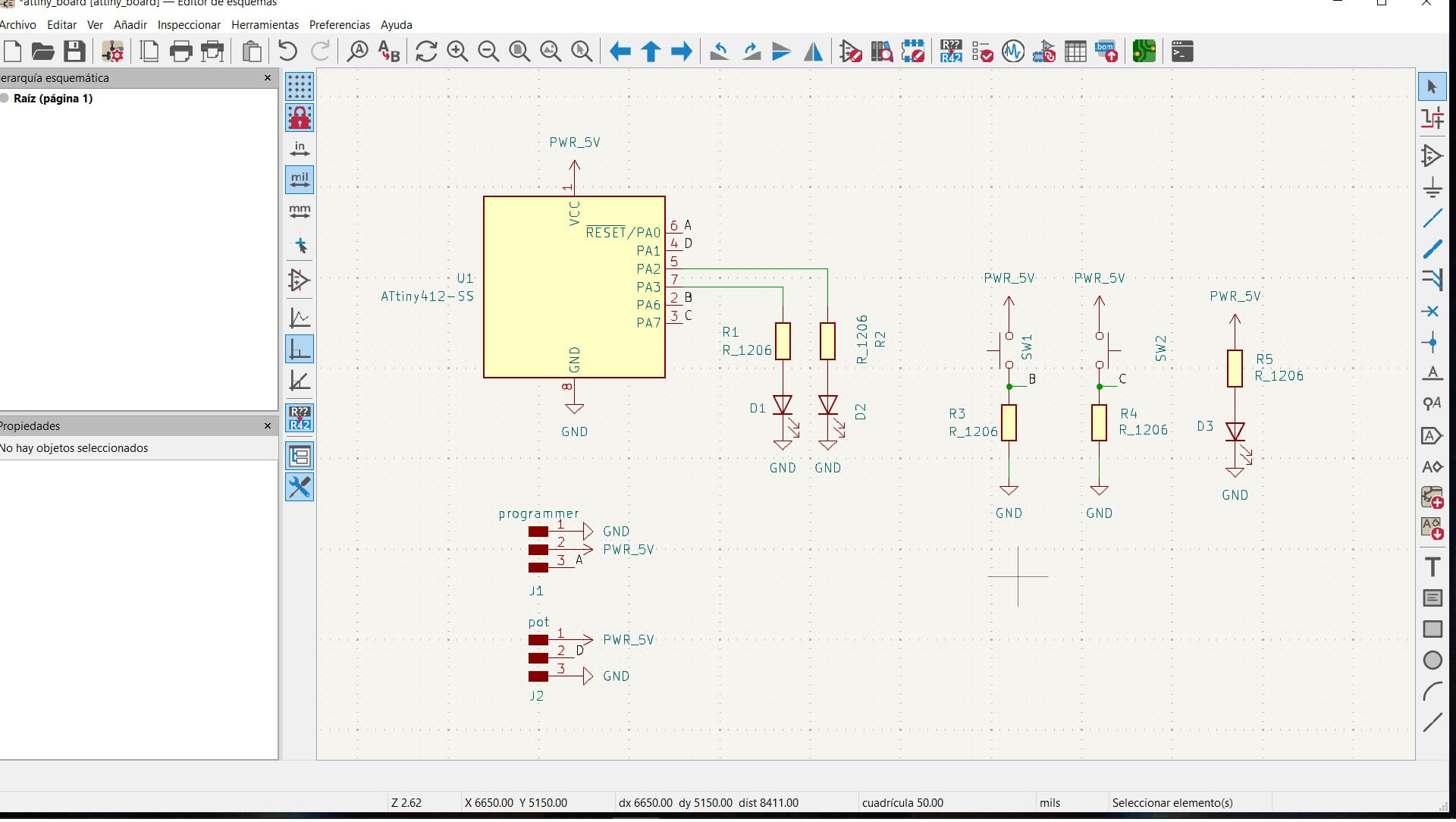
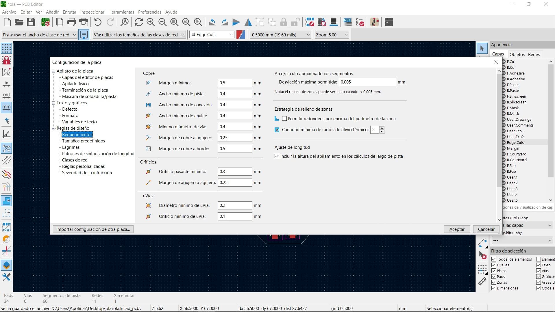
Likewise, here are the calculations for the minimum trace width, which resulted in 0.17 millimeters. Due to the complexity of soldering, I decided to use a thickness of 4 millimeters.
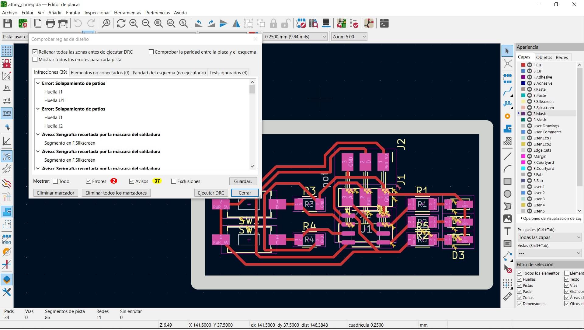
Then, I adjusted the board's requirements to my preference. That said, I must mention that I did't perform any calculations, since the voltage and current used in this case are very low. I placed the components in this way to make assembling the board physically with a CNC machine more convenient.
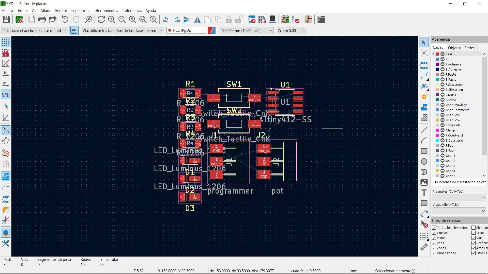
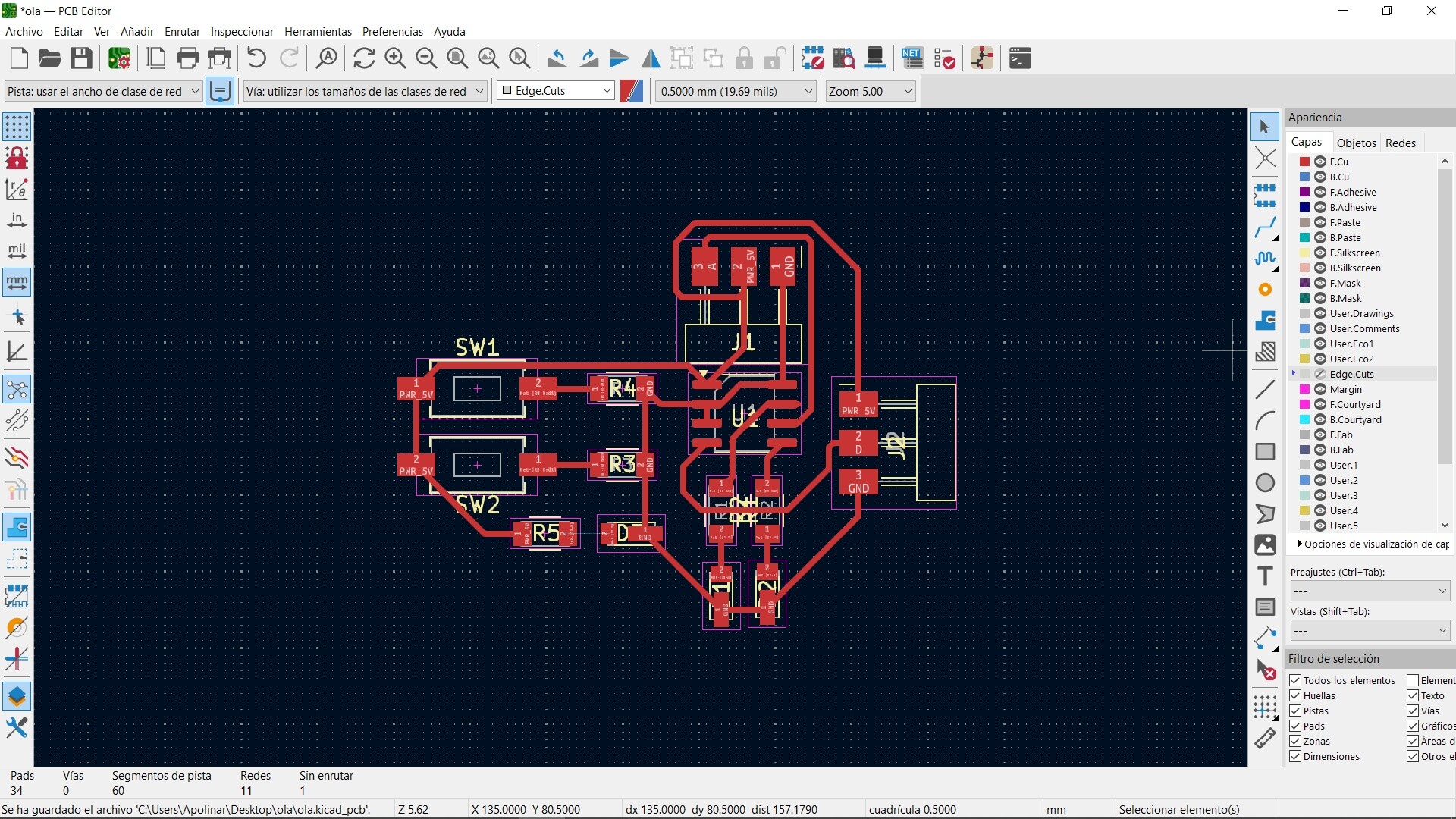
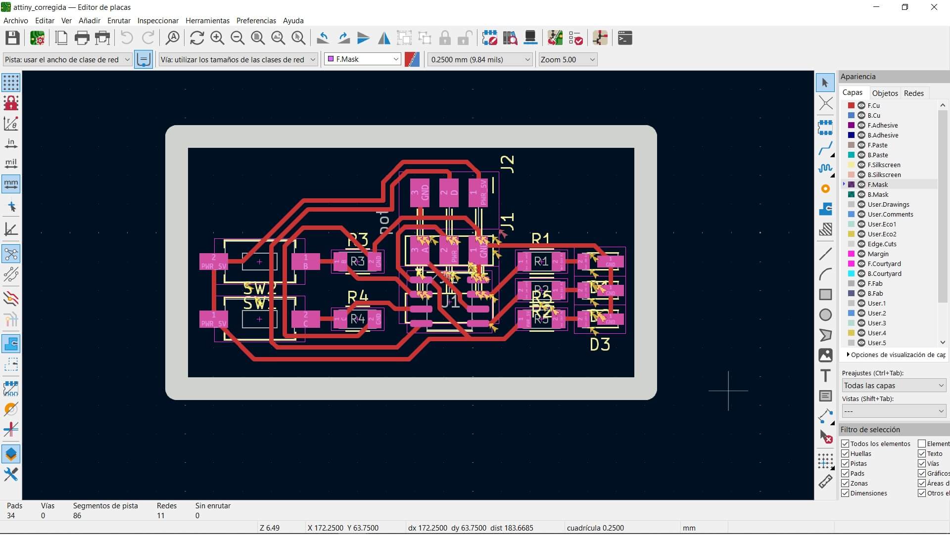
Next, I arranged the board as shown in the images, and I defined the cutting area with a polygonal line. There might be a more comfortable or efficient distribution, but I am unaware of it since I haven't done this many times.
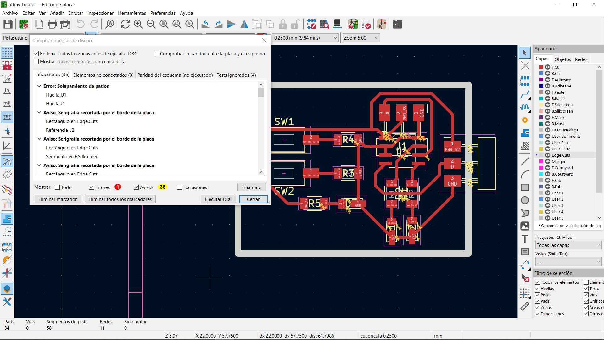
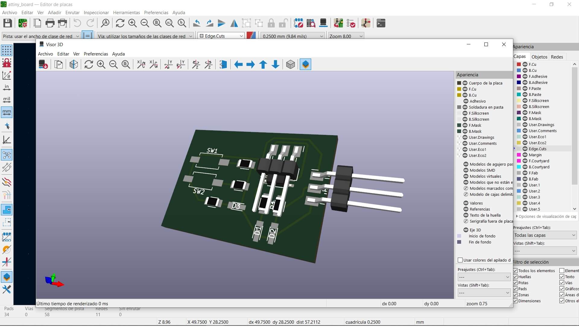
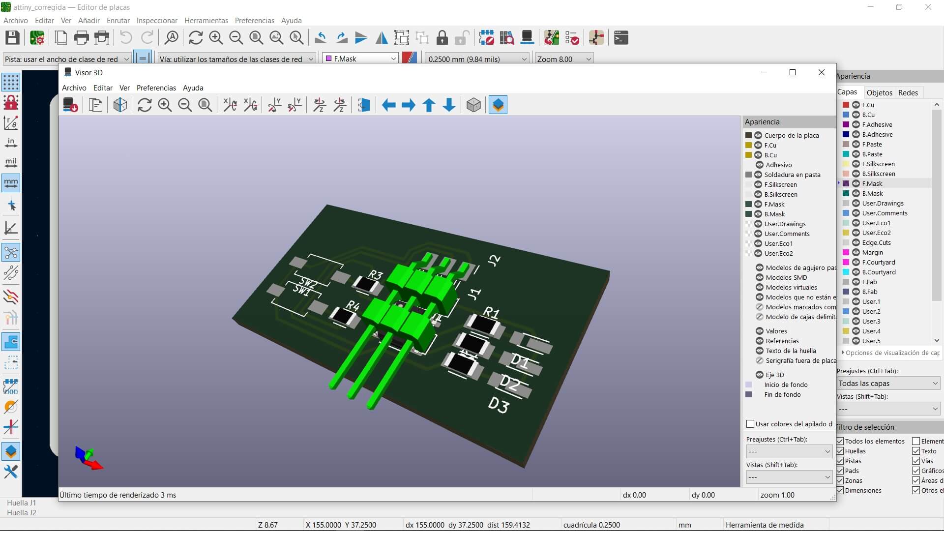
Here are the ERC and DRC. In the ERC, it shows 2 connection errors for GND and VCC, but it's not important since the connections are actually made. However, there is a connection warning for pin C, which I will need to change. In the DRC, I have many warnings that the silkscreen will be cut by the solder mask, but it's not important because these are elements I won't include on the board. On the other hand, the "Courtyard Overlap" errors are also not important since, unlike how it appears in my 3D image, the components will not be placed that way. Since I know exactly how I will position them when soldering, there will be no issues. The only things that will be present are the copper traces.
This is how the board should look if done correctly. Although some 3D models do not appear and one of the pins is on top of the Attiny, I can change that when soldering it onto the board, so it is not a major problem.
Since I realized that the buttons were incorrectly connected, I decided to remake the board. Here are the verifications with the same errors, except for the incorrectly connected buttons. However, the board is now correctly made with all the previously calculated parameters.
The really difficult part of this week was not making the board or thinking about the electronics, because to be honest, it is a very simple board but that's better than nothing. The hard part was figuring out what I was going to do, which ultimately led to the development of this board.
Here you have the link to our group page
