10. Mechanical design, machine design
Group assignment:
-
Design a machine that includes mechanism + actuation + automation + application
-
Build the mechanical parts and operate it manually.
-
Actuate and automate your machine.
-
Document the group project
To see our group assignment click here
Individual assignment:
- Document your individual contribution.
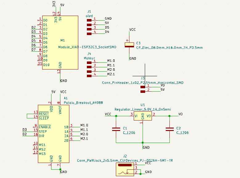
For this week’s assignment, we chose to design a turntable to facilitate 3D object scanning. Click here to access the group’s work page. To make this machine, I designed the printed circuit board that will control it. Generally speaking, we chose to use a XIAO ESP32C3 with an OLED screen, combined with A4988 drivers to control a NEMA 17 stepper motor.
Design circuit board
For the PCB design we used Kicad, for more details see Week 6.
we have chosen to use the following components for our printed circuit board :
| Device | Parts | Value | Qty |
|---|---|---|---|
| Pololu_Breakout_A4988 | A1 | 1 | |
| PinHeader_1x04_P2 | J1 | 1 | |
| Conn_PWRJack_2x5.5mm | J2 | 1 | |
| PinHeader_1x02_P2 | J3 | 1 | |
| UNPOLARIZED_CAPACITOR | C1 | 10uF | 1 |
| UNPOLARIZED_CAPACITOR | C2 | 1uF | 1 |
| CP_Elec_D8.0mm_H16.0mm_TH_P3.5mm | C3 | 100nF | 1 |
| PinHeader_1x04_P2 | J4 | 1 | |
| SeeedStudio_XIAO_SocketSMD | U1 | 1 | |
| Regulator_Linear_5.0V_1A_OnSemi | U2 | 1 |
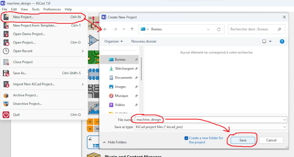
- Open KiCad 7.0 click on File>New project
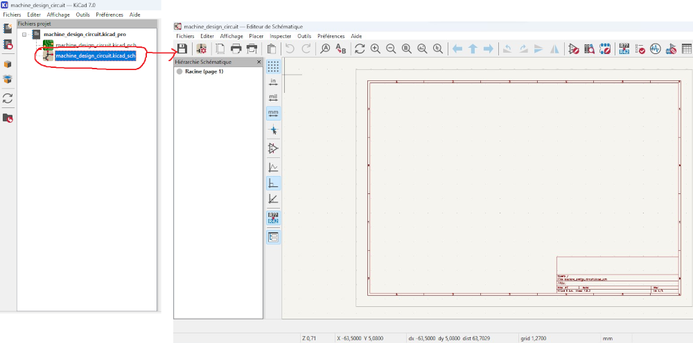
- Double left-click on the file circled in red below to access the electronic schematic entry page.
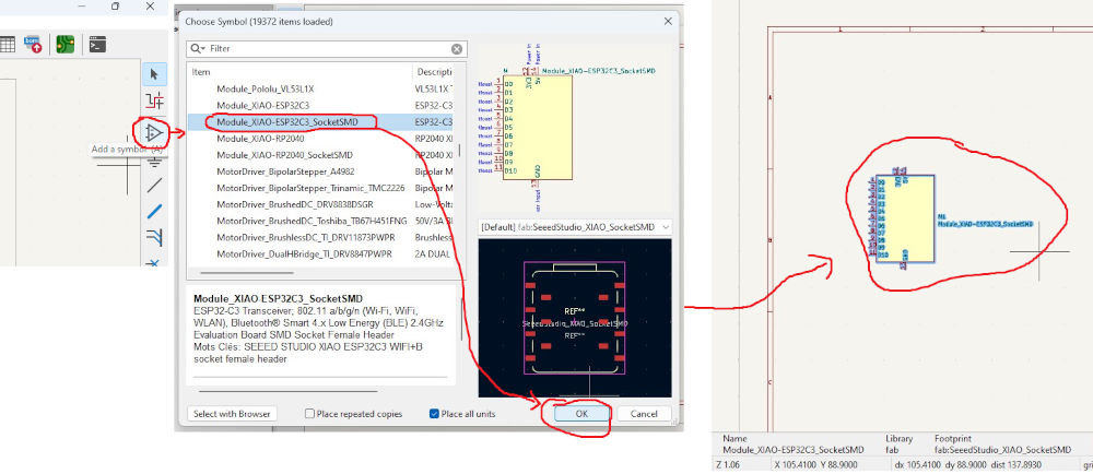
- To add components, click on the icon circled in red. A window will open, select your component, click on ok and place it in the schematic input zone as shown below.
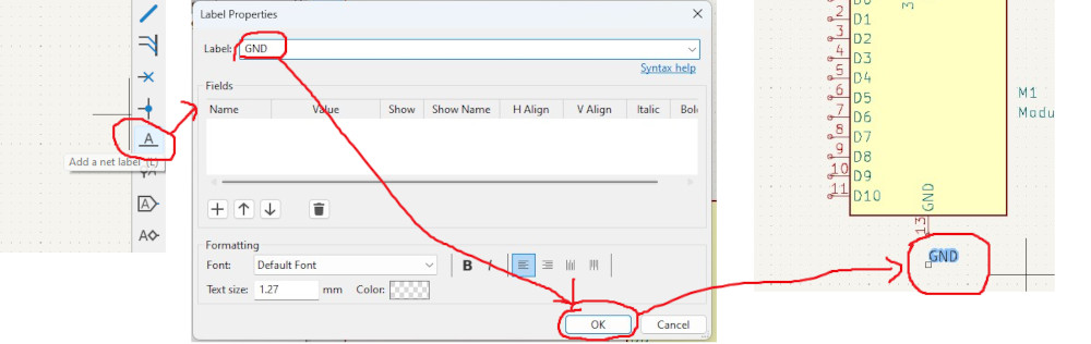
- After placing the component, we used the “add a net label (L)” tool as shown above. to use it, click on it and enter the markers of the terminals you want to use as shown below.
- Now we’re going to connect the XIAO’s GND terminal to the GND label. To do this, position yourself on the end of the XIAO’s GND terminal as shown below and click on it, then move the mouse to the GND label terminal and click a second time on the mouse.
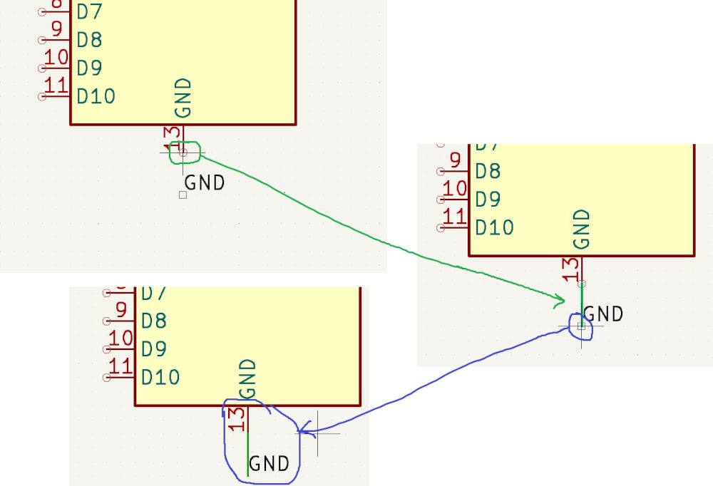
- After following and repeating the steps described above, we obtained the following result.
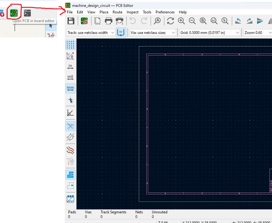
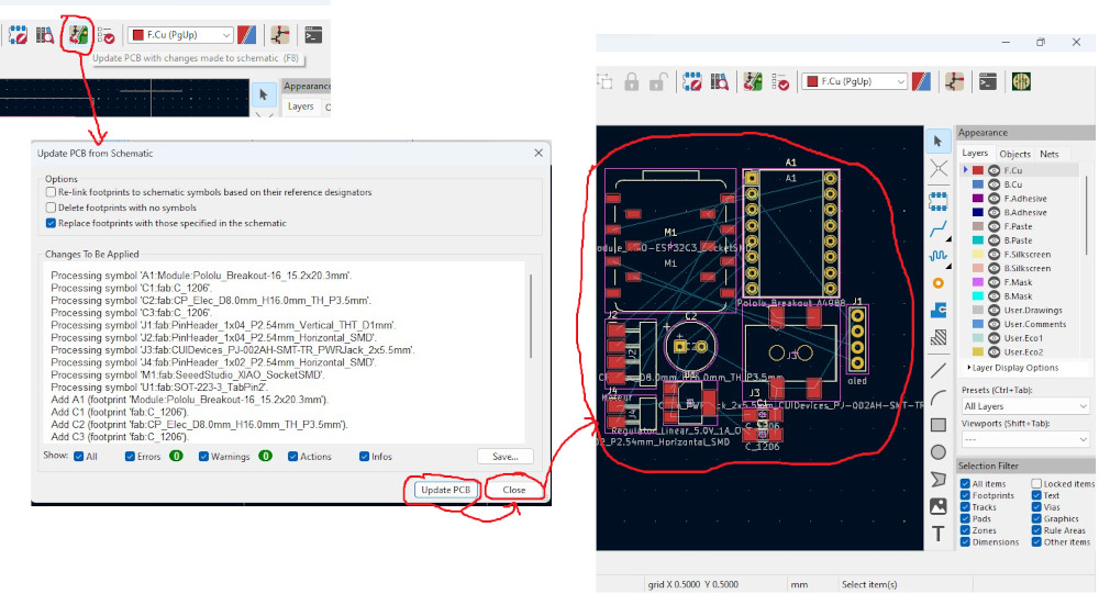
Now that we’ve finished the circuit diagram, we’ll move on to the PCB design. To do this, click on the icon circled in red below.
- Once the PCB window is open, click on the icon circled in red below, then on update and on close, and place the traces of the various components where you want them, as shown below.
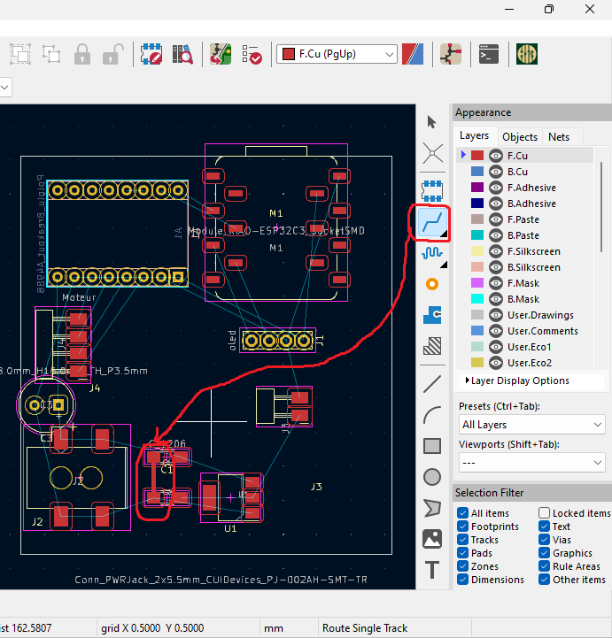
Once you have positioned the components correctly and resized the edges of the PCB as shown above, click on “route tracks (X)” to trace the PCB tracks as shown below.
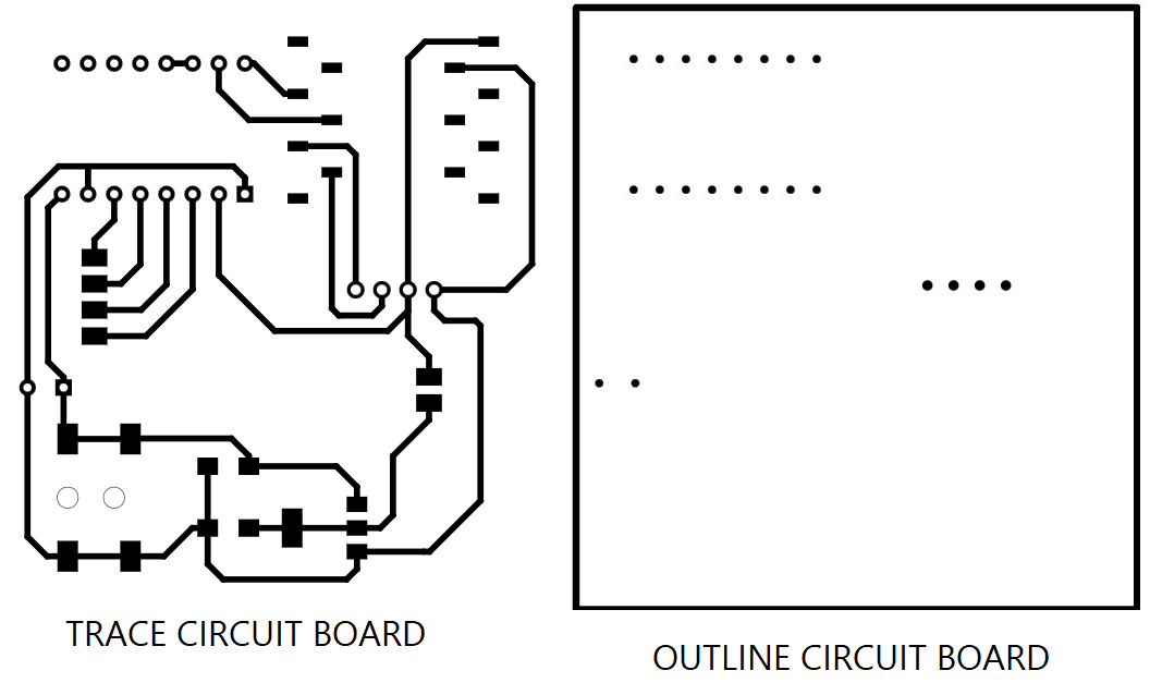
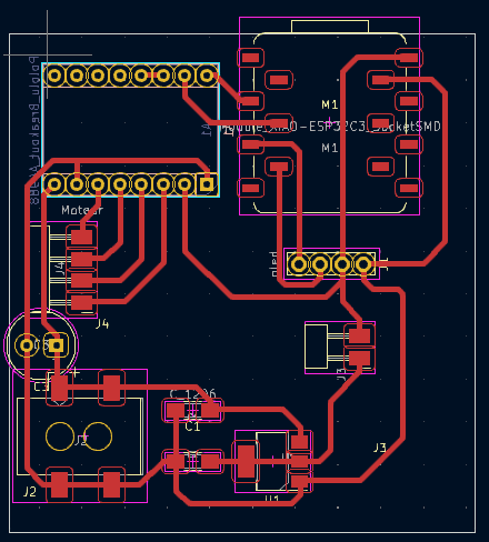
- After tracing all the tracks on the printed circuit board, we obtained the result below.
Generation of SVG files for the traces and the board outline
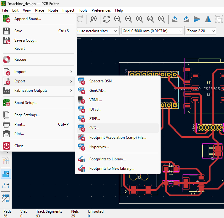
Once all the components have been placed and the tracks assembled, I need to export the file in “.SVG” format. We exported only the tracks, then the contours. To do this, we follow the procedure below:
- Click on File> Export> SVG…
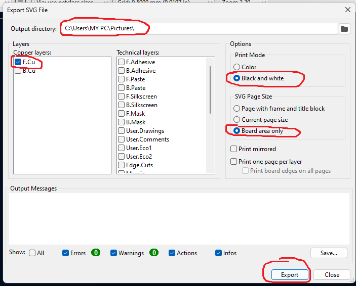
- First, we’ll export the PCB traces.To do this, in the export window, check the “F.Cu” , “Black and White” and “Board area only” boxes as shown below and click on Export.
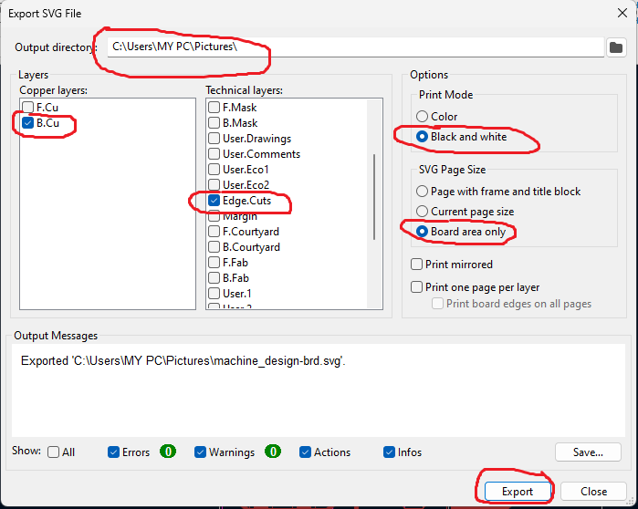
- To export the PCB contours and holes, check the “B.Cu” , “Edge.Cuts”, “Black and White” and “Board area only” boxes as shown below and click on Export.
Below is an image of the export results. To obtain the design and SVG source files for the printed circuit board, go to the Files section at the end of the page.