6. Electronics design
Group assignment:
- Use the test equipment in your lab to observe the operation of a microcontroller circuit board(as a minimum, you should demonstrate the use of a multimeter and oscilloscope)
To see our group assignment click here
Individual assignment:
-
Design a development board to interact and communicate with an embedded microcontroller
-
extra credit: try another design workflow; make a case for it; Simulate its operation
For our individual assignment this week we have chosen to design the electronic board of our final project which will contain the microcontroller ESP32-WROOM-32D-N4.
For the design of a printed circuit there are various software namely: Autodesk Eagle, Altium Designer, Proteus, Kicad, EasyEDA,UPVERTER…
In our case we chose the software Autodesk Eagle for the design of our printed circuit boards. In the following we will show how we designed our PCB with Autodesk Eagle.
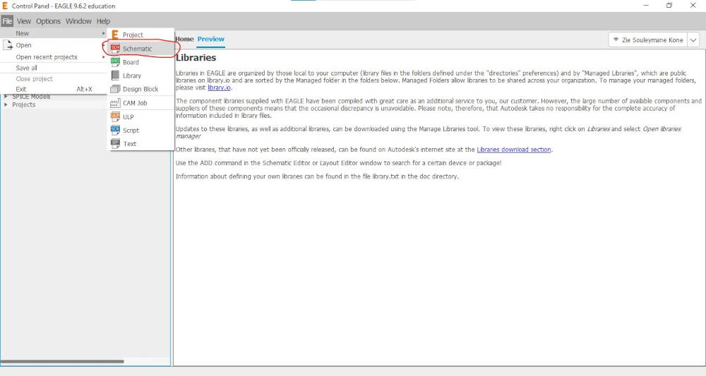
Installation Autodesk Eagle
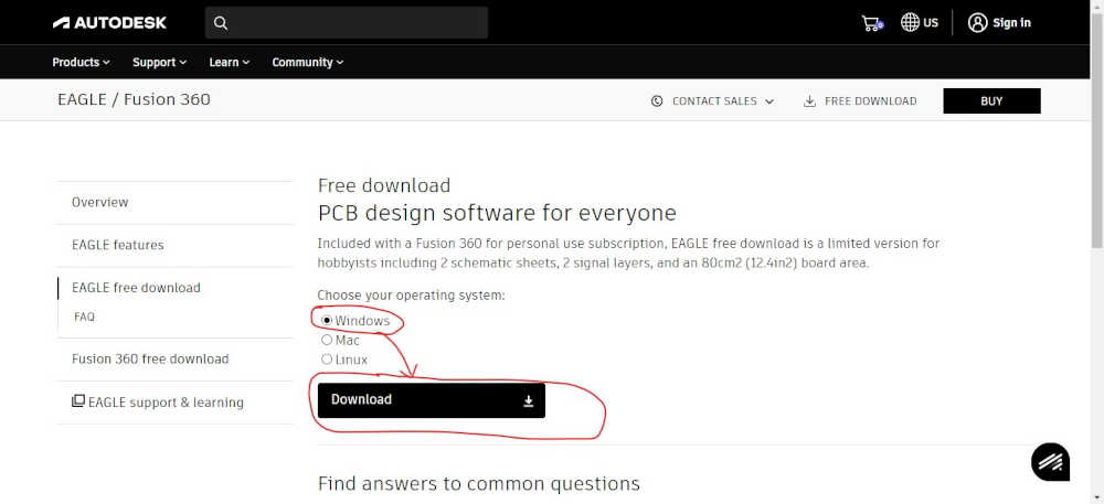
To download Autodesk Eagle click here
Once on the site select the Windows option and click on Download.
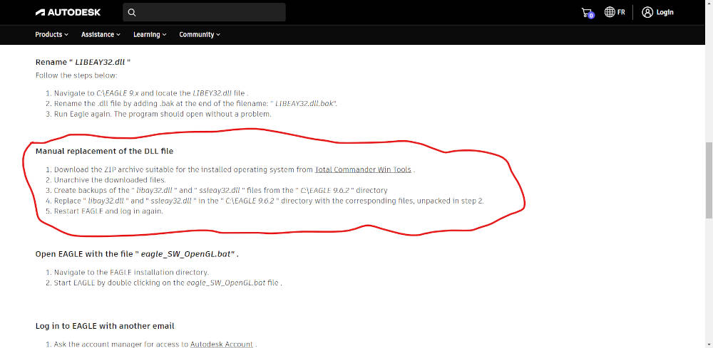
After installing the software and connecting our email we encountered a problem. Autodesk eagle closes abruptly after the welcome screen and does not start.
To solve this problem we used the solution circled in red below. The solution is available at the link Autodesk Eagle solution
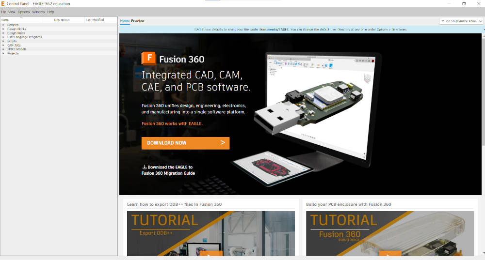
After solving the problem of starting the software you should have the following display.
Installation of libraries
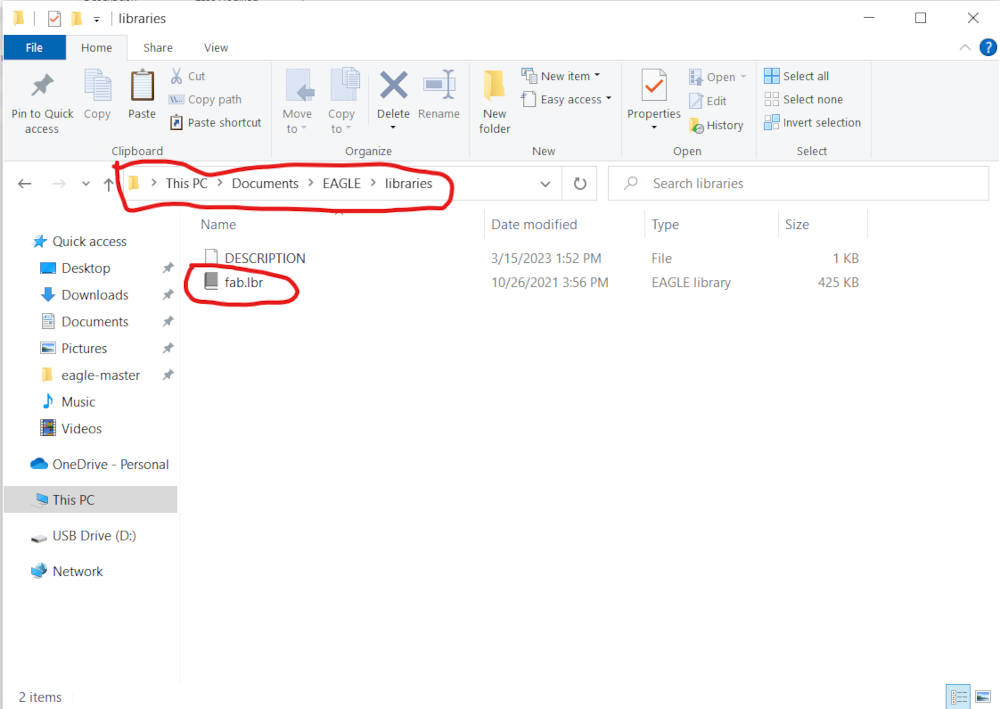
For the realization of our printed circuit with Autodesk eagle we have downloaded the Fab library at the link Eagle Fab library as shown below.
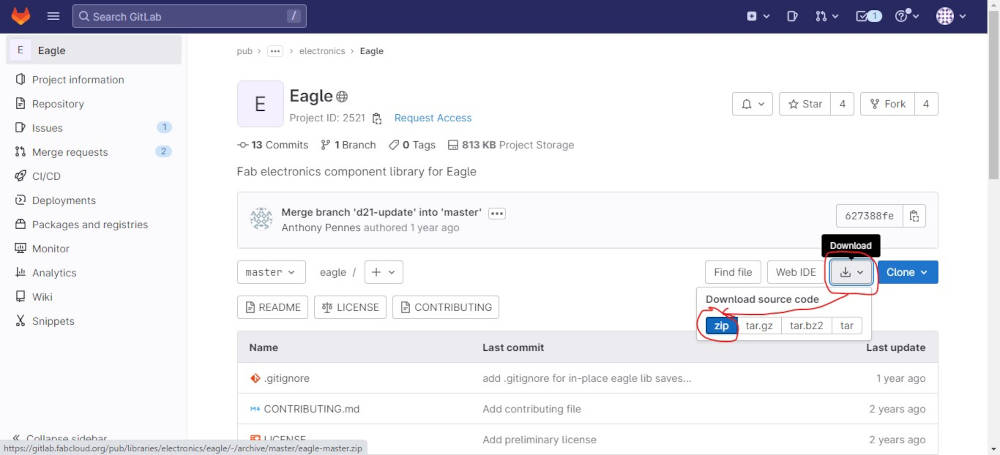
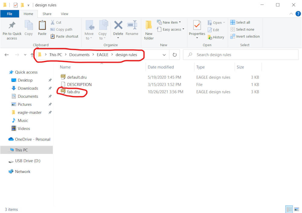
Unzip the downloaded zip file and copy the files “fab.lbr” and “fab.dru” in the directory indicated below.
Design circuit board
Before starting the design of our circuit we made a study on the ESP32 microcontroller to select the useful pins for our project and the basic components needed to make it work. We started by consulting the ESP32 datasheet available here, in which we were first interested in the description and function of each pin of the ESP32. This allowed us to choose the terminals of the ESP32 that we will use.
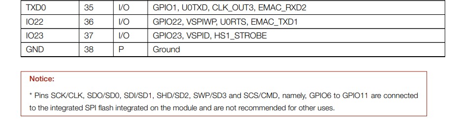
While reading the datasheet we noticed an important note on the terminals that are recommended not to be used as below.
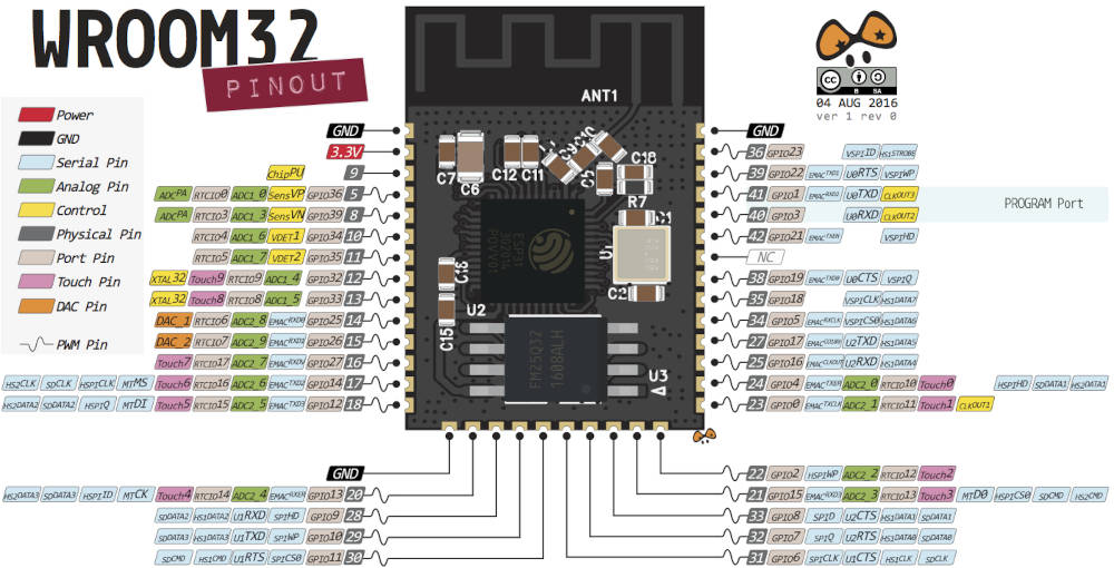
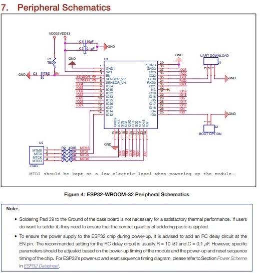
Another important information in the datasheet is the point Peripheral Schematics (Page 19) it gives us recommendations on the basic elements to make the ESP32 work.
Still looking for the basic components to make our ESP32 work properly we consulted the link concerning hello.ESP32 available in the embedded_programming section of the fab academy. Here is what we found below.
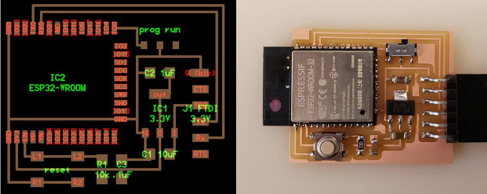
After comparing the schematic proposed in the datasheet and the schematic of hello.ESP32 we have chosen to use the following components for our circuit board :
| Device | Parts | Value | Qty |
|---|---|---|---|
| 6MM_SWITCH | S1 | 1 | |
| LED | LED | 1 | |
| RESISTOR | R1 | 100 | 1 |
| RESISTOR | R3 | 10k | 1 |
| UNPOLARIZED_CAPACITOR | C1 | 10uF | 1 |
| UNPOLARIZED_CAPACITOR | C2 | 1uF | 1 |
| UNPOLARIZED_CAPACITOR | C3 | 100nF | 1 |
| ESP32-WROOM | ESP32 | 1 | |
| REG_LM1117SOT223 | U1 | 1 | |
| SLIDE-SWITCH | S2 | 1 | |
| 10_PIN_HEADER | U$3 | 1 | |
| 10_PIN_HEADER | U$4 | 1 | |
| FTDI-SMD-HEADER | U$5 | 1 | |
| FTDI-SMD-HEADER | U$6 | 1 |
- Open Autodesk Eagle click on File>New>Schematic
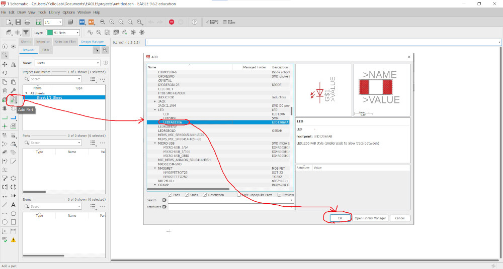
- Click on the “Add Part” button and select the “LEDFAB1206” component as shown below.
- After adding a second component which is a resistor click on “Net” to connect the different components as shown below.
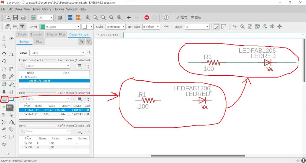
- Click on “Name” and rename the green lines as shown below.
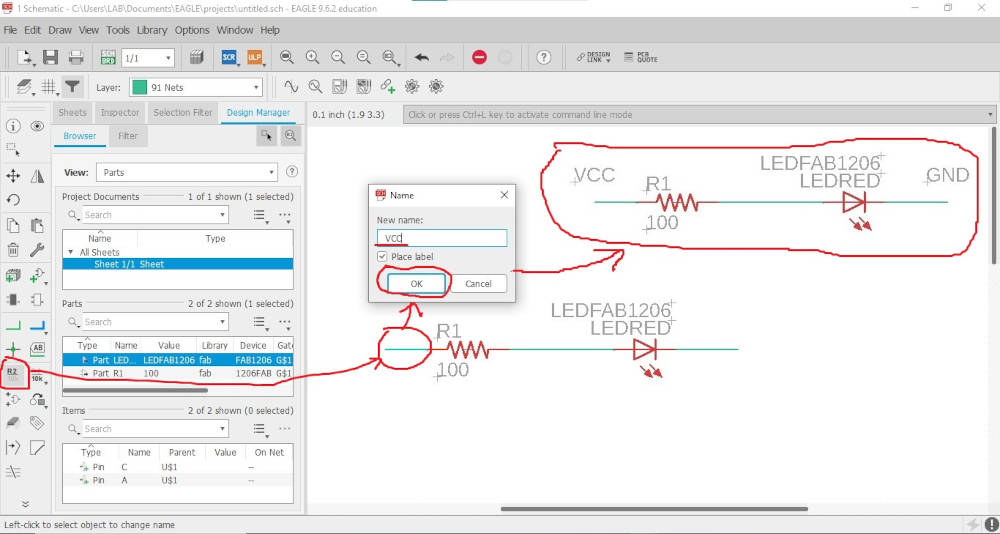
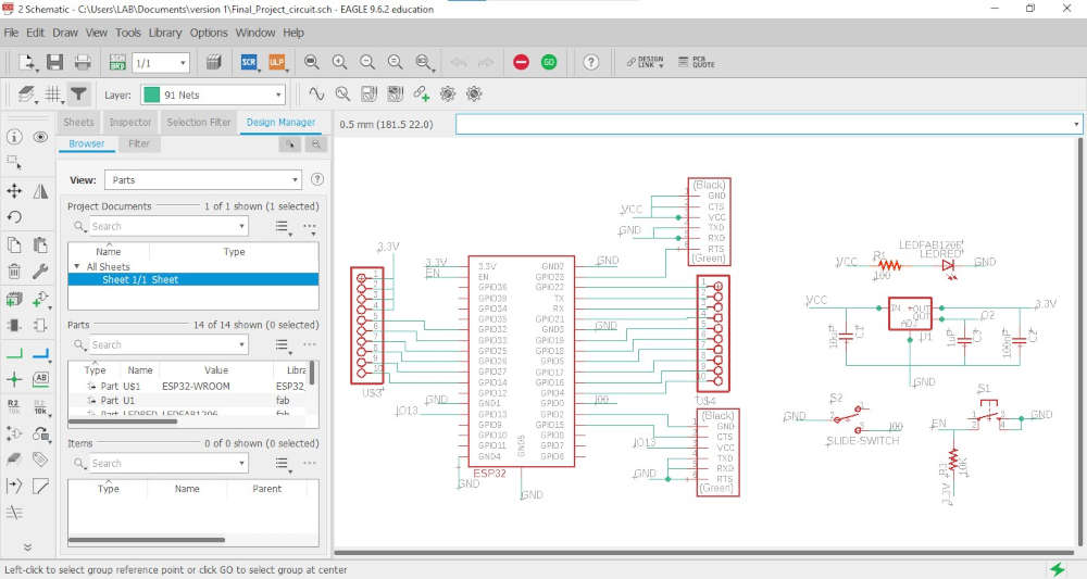
- We repeat all the above procedures to obtain the final result below
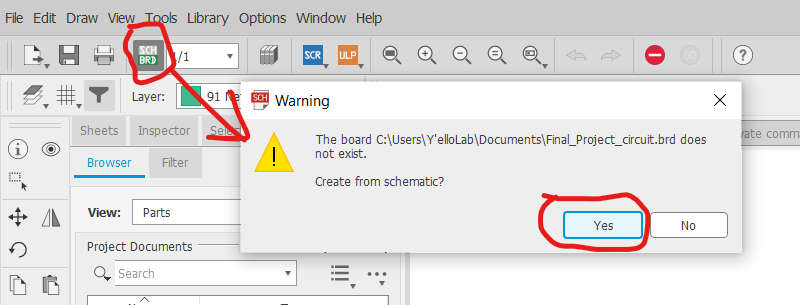
We have finished the drawing of the electronic schematic and now we will draw the PCB.
- Click on the “Generate/switch to bord” button and click on “Yes” you should have the following display.
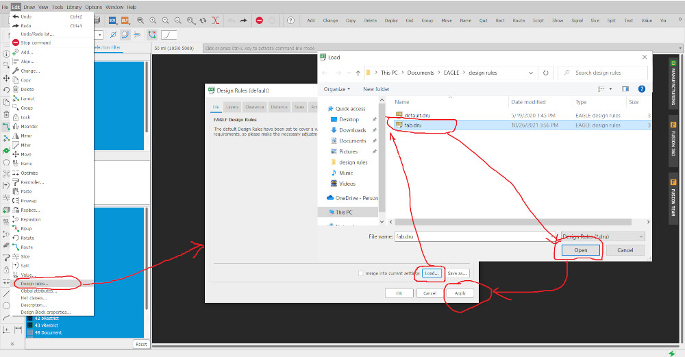
- Go to “Edit” and click on “Design rules…” a window will appear click on “Load” and choose “fab.dru” click on “Open” and then on “Apply”
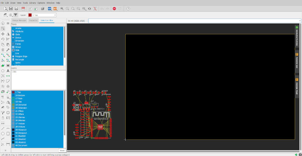
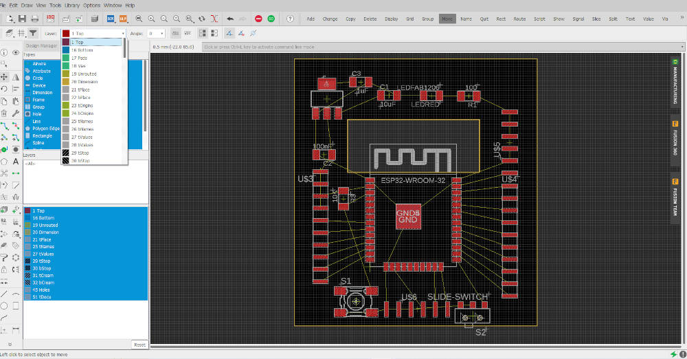
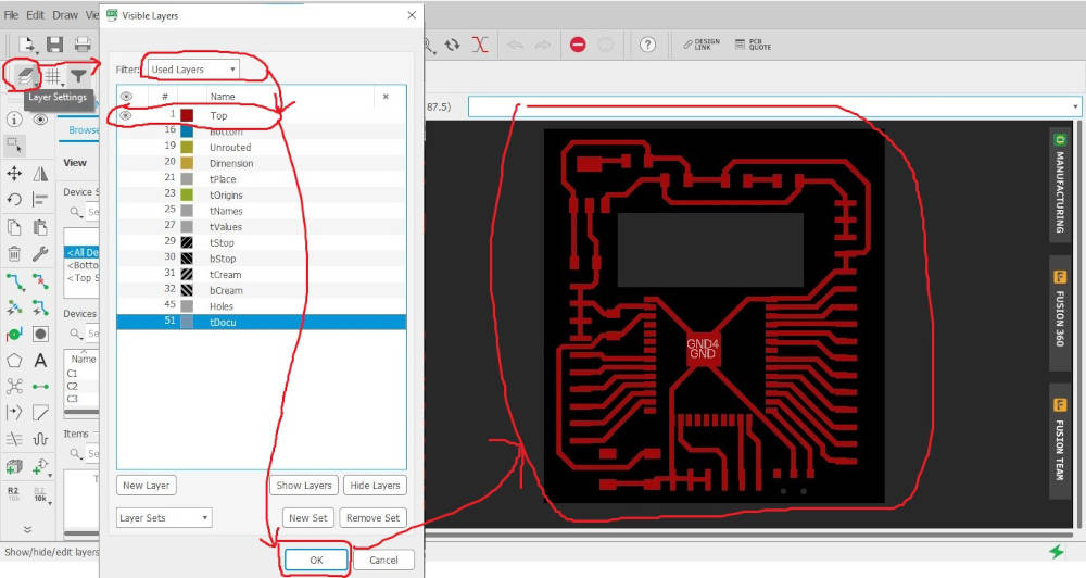
- After positioning the components correctly and resizing the borders of the PCB. In “layer” select the “Top” option as shown below.
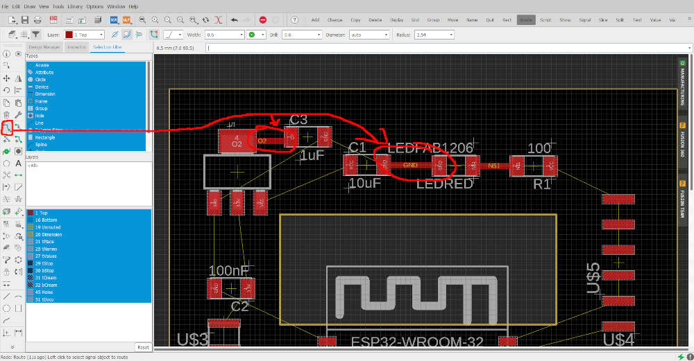
- Select the “Route Airwire” tool and draw the different tracks of the circuit as shown below
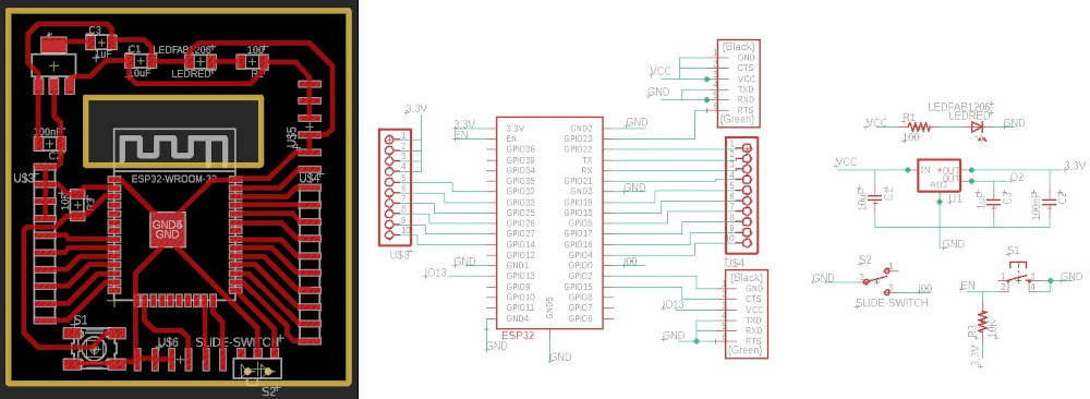
Here is our electronic schematic and our PCB after we finished our design.
Generation of PNG files for the traces and the board outline
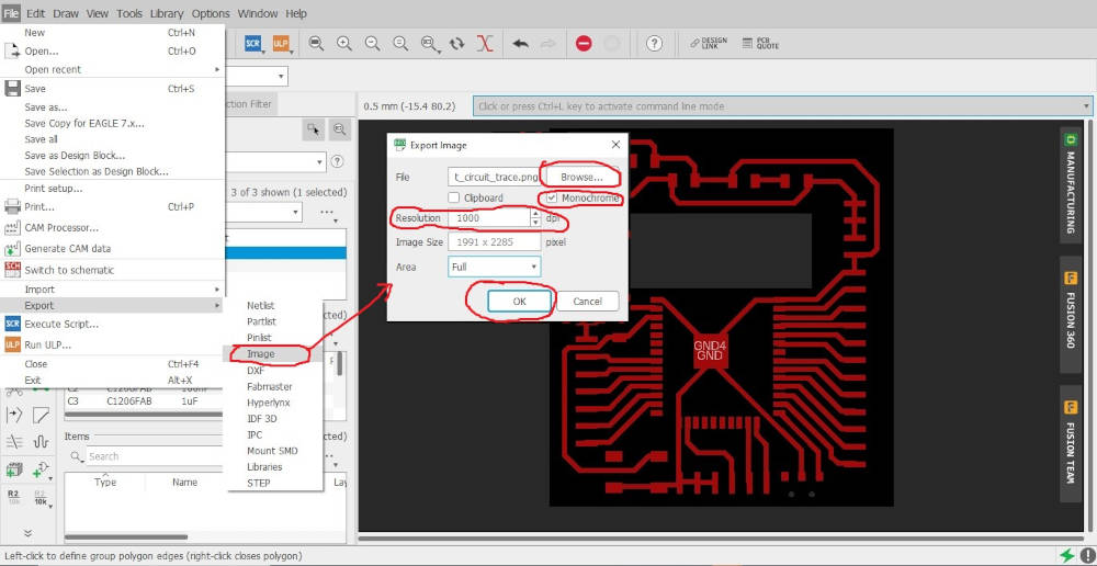
Once I have all the components placed and the tracks together, I need to export the file as a “.PNG”. But first we need to be only exported the tracks, and after the outlines. To do this we followed the process below:
- Click on “Layer Settings”, go to “Filter” select “Used Layers” and uncheck all but “Top” and click on “OK”.
- Go to File>Export and click on “Image” a window will open, click on “Browse…” to choose the file type and location, select “Monochrome” with Resolution = 1000 dpi and click on “OK”.
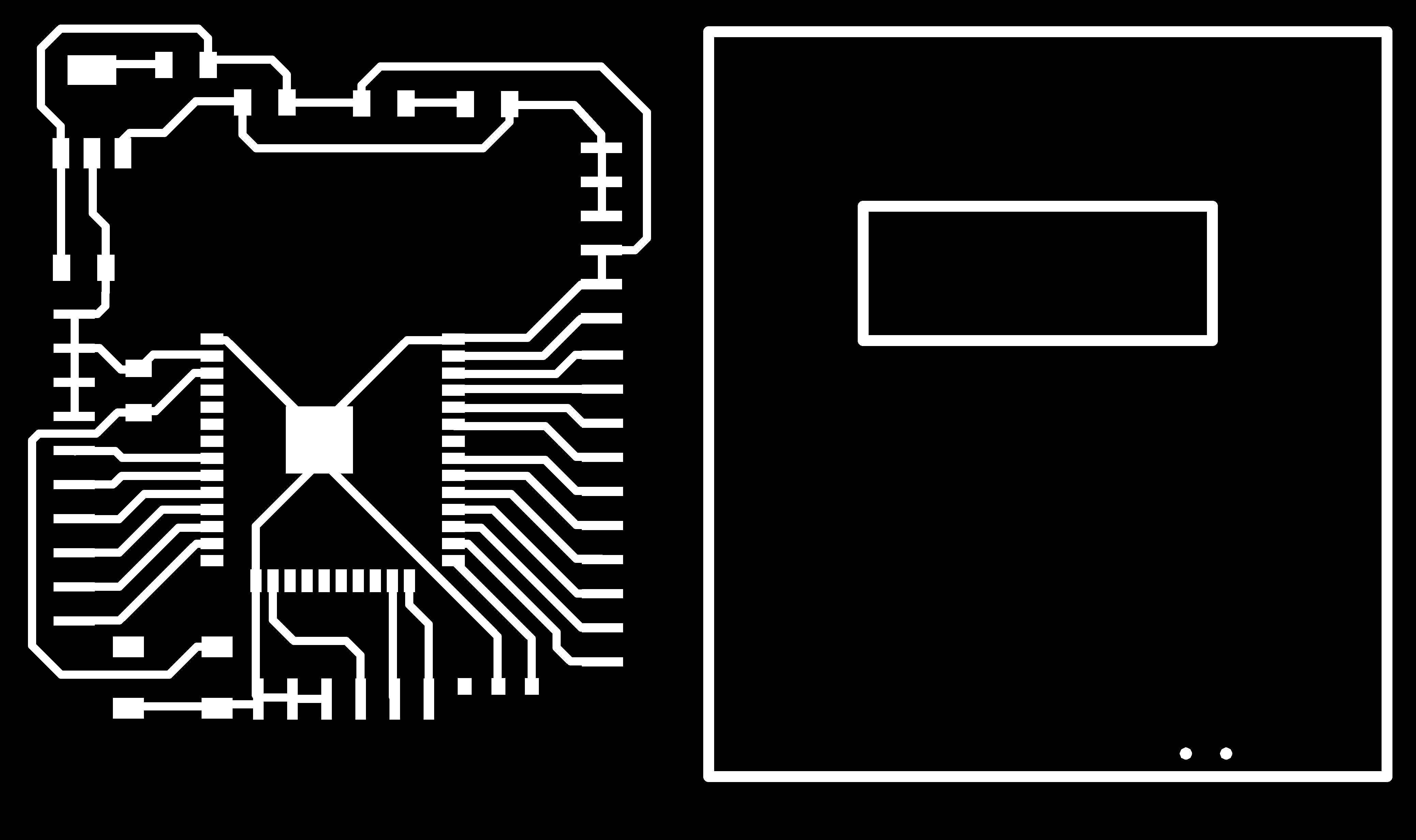
- Repeat the same procedure as above and in “layer settings” select “Dimension” instead of “Top”.
You should have the results below.
Click here to download the PNG files.
Links
-
https://learn.sparkfun.com/tutorials/using-eagle-schematic/all
-
https://maker.pro/custom/tutorial/autodesk-eagle-for-beginners-basics