WEEK 06. Electronics design
Assignment
.group project:
Use the test equipment in your lab to observe the operation of a microcontroller circuit board(as a minimum, you should demonstrate the use of a multimeter and oscilloscope)
.individual project:
  design a development board to interact and communicate
  with an embedded microcontroller
  extra credit: try another design workflow
  extra credit: make a case for it
  extra credit: simulate its operation
Autodesk Eagle
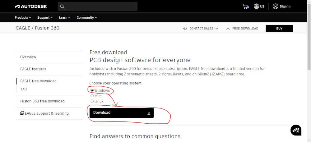
To download Autodesk Eagle click here Once on the site select the Windows option and click on Download.
Installation of libraries
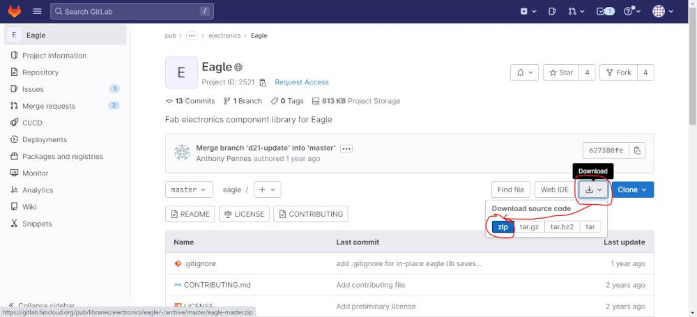
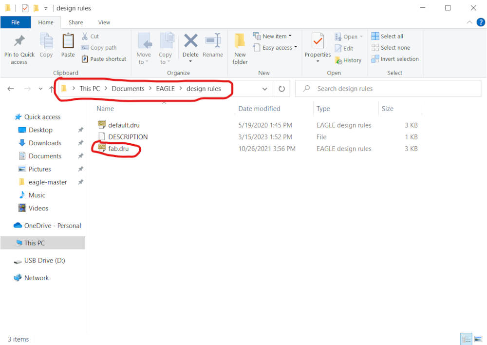
For the realization of our printed circuit with Autodesk eagle we have downloaded the Fab library at the link Eagle Fab library as shown below.
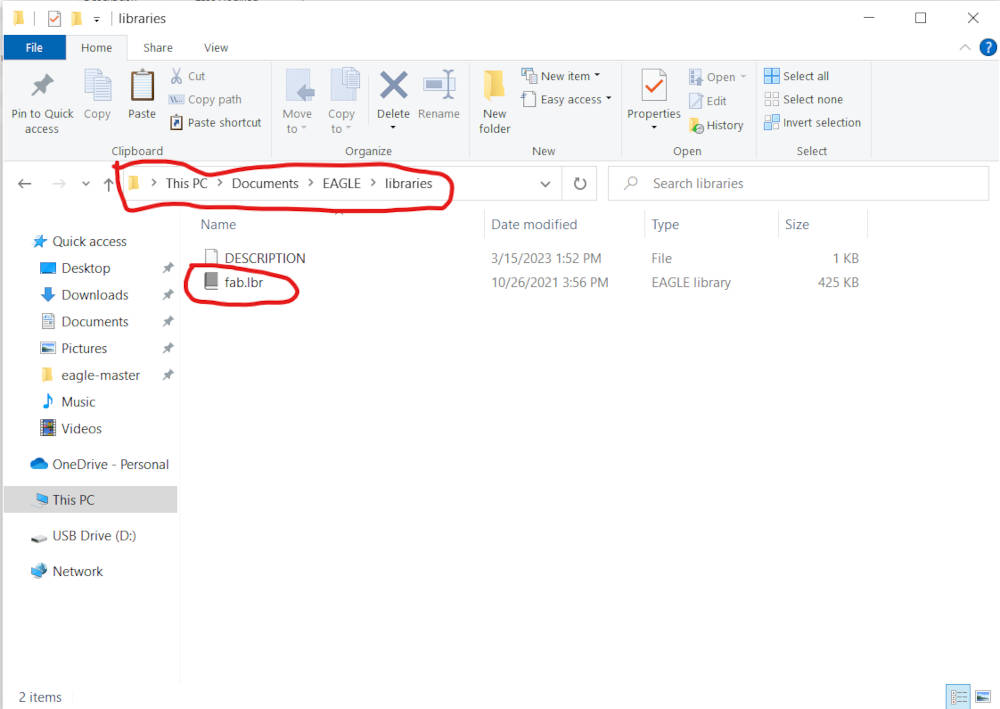
Unzip the downloaded zip file and copy the files “fab.lbr” and “fab.dru” in the directory indicated below.
For our PCB design we used the Seeed Studio XIAO ESP32-C3.
Data sheet : Seeed Studio XIAO ESP32-C3
Presentation
Seeed Studio XIAO ESP32C3 is a development board for microcontrollers. It features an Espressif ESP32-C3 WiFi/Bluetooth dual-mode chip with a size of 20 x 17.5 mm, suitable for small projects and portable thanks to its low power consumption.
Specification
| Item | Value |
|---|---|
| CPU | ESP32-C3 32-bit RISC-V @160MHz |
| Wireless Connectivity | WiFi and Bluetooth 5 (LE) |
| Flash Memory | 4MB |
| SRAM | 400KB |
| Digital I/O Pins | 11 |
| Analog I/O Pins | 4 |
| PWM Pins | 11 |
| I2C interface | 1 |
| SPI interface | 1 |
| UART interface | 2 |
| Power supply and downloading interface | Type-C |
| Power | 3.3V/5V DC |
| Dimensions | 20×17.5×3.5mm |
More information in this link. Here the Seeed Studio XIAO ESP32C3 pinout sheet.
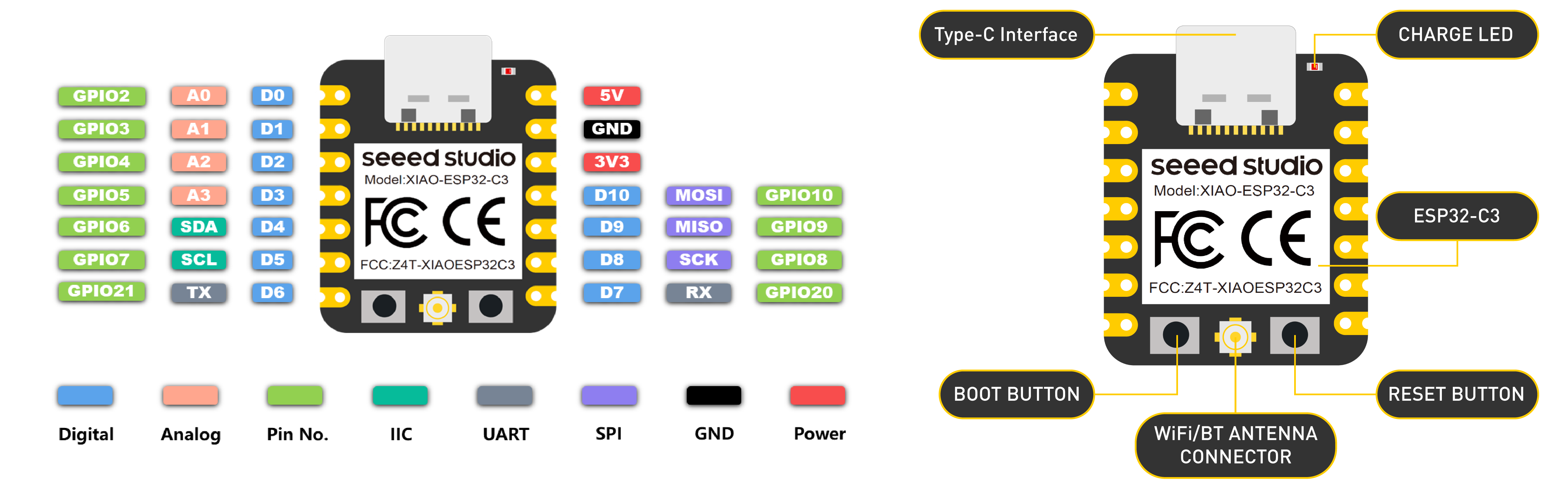
- 5V: Supply voltage 5V.
- GND: Ground.
- 3V3: Supply voltage 3V3.
- Digital pins (GPIO Pin number): D0, D1, D2, D3, D4, D5, D6, D7, D8, D9, D10, D11
- Analog pins (GPIO Pin number): A0, A1, A2, A3
- SDA (GPIO Pin number): D4
- SCL (GPIO Pin number): D5
Note
Below are some important notes on the terminals of the XIAO ESP32C3 board, which should be taken into account when using it. For more details, click here.
- Terminal D9 of the XIAO ESP32C3 is connected to GPIO9 of the ESP32-C3, to a pull-up resistor and to the BOOT button. So pressing the BOOT button connects D9 to GND. It is therefore preferable to use D9 as a switching input.
- D6 on the ESP32C3 XIAO is connected to U0TXD (28) on the ESP32-C3. D’ou D6 is configured as a UART output at start-up, so if you use D6 as an input, you may accidentally generate a high current. So it is recommended to use the D6 pin only in output mode.
BOM and Schematic
Samdino |
Where to buy? | Amount | Price | Total price |
| Proto Board FR1 | Digikey | 1/4 board | 1,24 €/unit | 0,31 € |
| Seeed Studio XIAO ESP32C3 | Seeed Studio | 1 | 5,00 €/unit | 5,00 € |
| 499 Ω resistor | Digikey | 1 | 0,09 €/unit | 0,09 € |
| 1kΩ resistor | Digikey | 1 | 0,09 €/unit | 0,09 € |
| LED | Digikey | 1 | 0,35 €/unit | 0,35 € |
| Button | Digikey | 1 | 1,00 €/unit | 1,00 € |
| Female 1 row horizontal header | Digikey | 3 | 0,15 €/unit | 0,45 € |
| Total cost | 7,29 € |
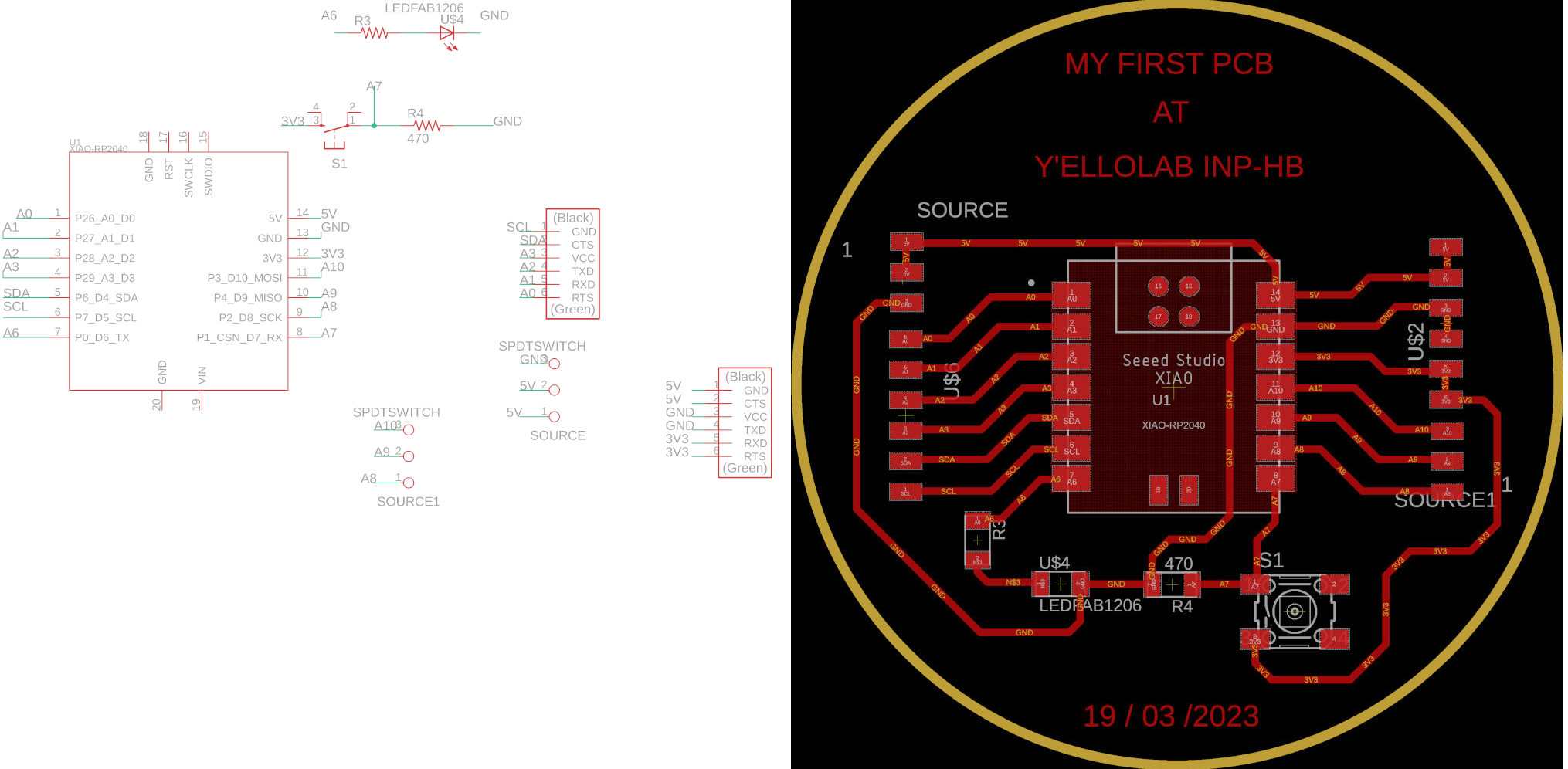
Design
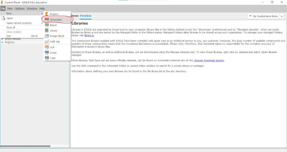
- Open Autodesk Eagle click on File>New>Schematic
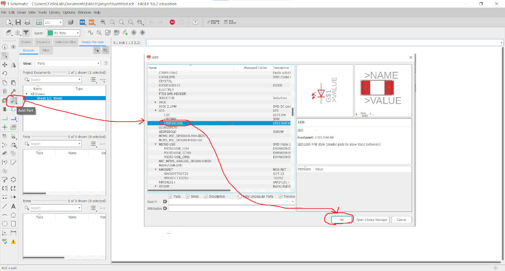
- Click on the Add Part button and select the LEDFAB1206 component as shown below.
- Once you’ve added all the components, click on Net to connect them as shown below.
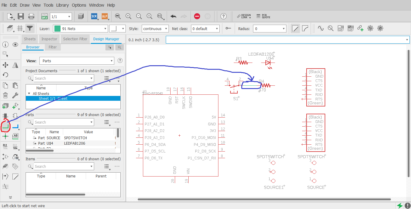
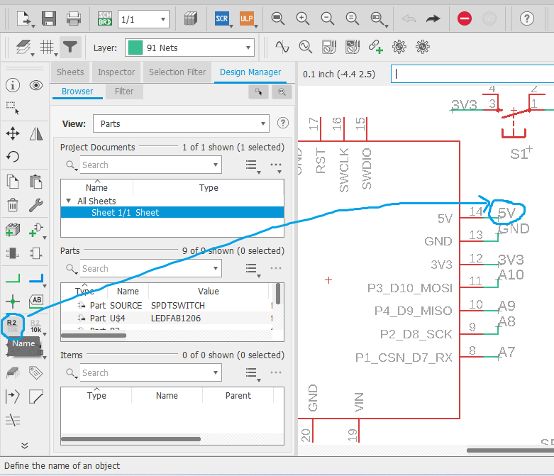
- Click on Name and rename the green lines as shown below.
- We repeat all the above procedures to obtain the final result below
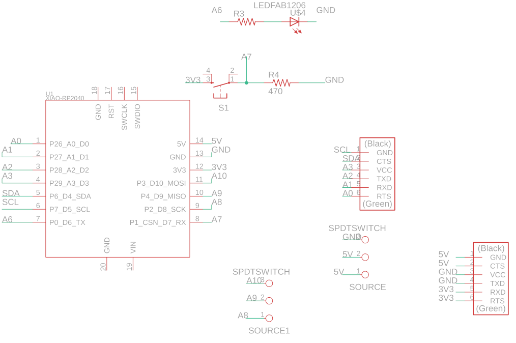
We have finished the drawing of the electronic schematic and now we will draw the PCB.
Switch to pcb by clicking on generate/switch to board on the top bar.
## TRACE PARAMETERS
The parameters of the board traces are shown below.
| Width | Drill | Clearance |
|---|---|---|
| 0.6mm | 0.6mm | 0.3mm |
In the parameters we have:
-
The width of the trace : I set to 0.6mm
-
Drill refer to the tool diameter. The tool I used is 1/64” i.e around 0.4 mm So I can set until 0.4 mm of drill parameter.
-
The clearance refer to the space between patterns more specifically the space enabled between two patterns. It is preferable to not set less than the tool diameter : I set to 0.3. It is more important to have the same value as the tool diameter if we do rastenest at the default settings on our board. In my case I did’nt do that.
-
In my case I created my own net classe which I set different parameters as highlighted below.

To display this window go to edit > Net classes To create new classe click on add you can see on the picture above.
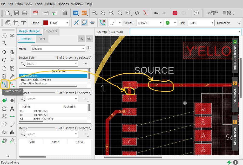
- After positioning the components correctly and resizing the edges of the PCB. Select the “Route Airwire” tool and draw the various circuit tracks as shown below.
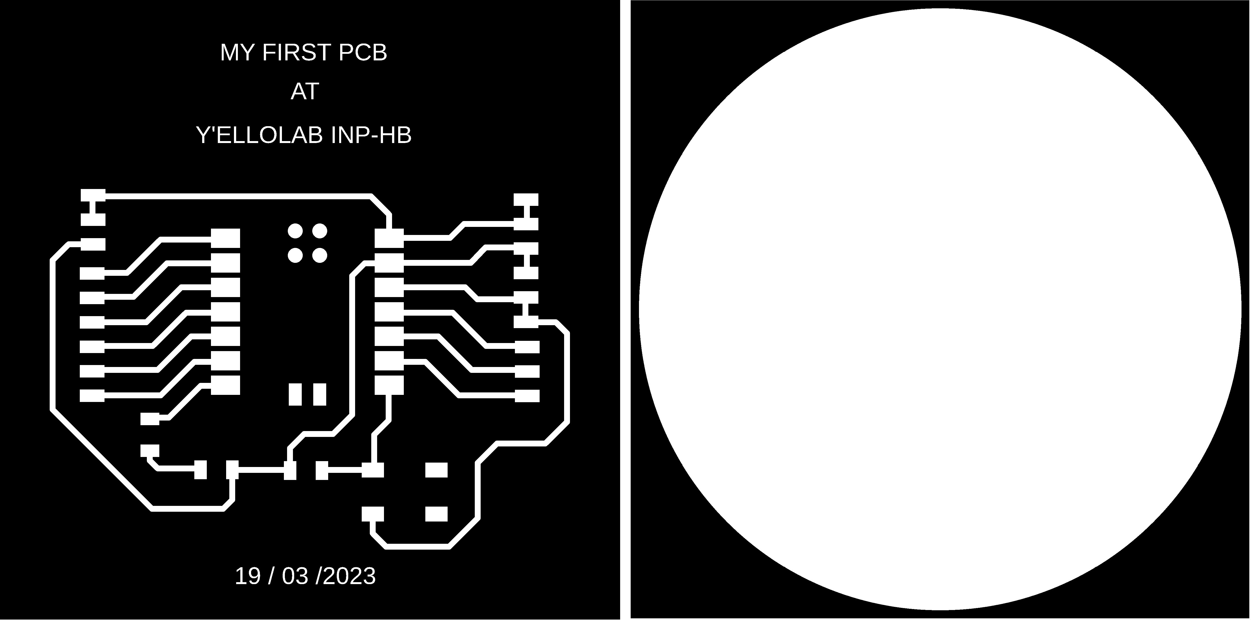
Here are the final results of our design
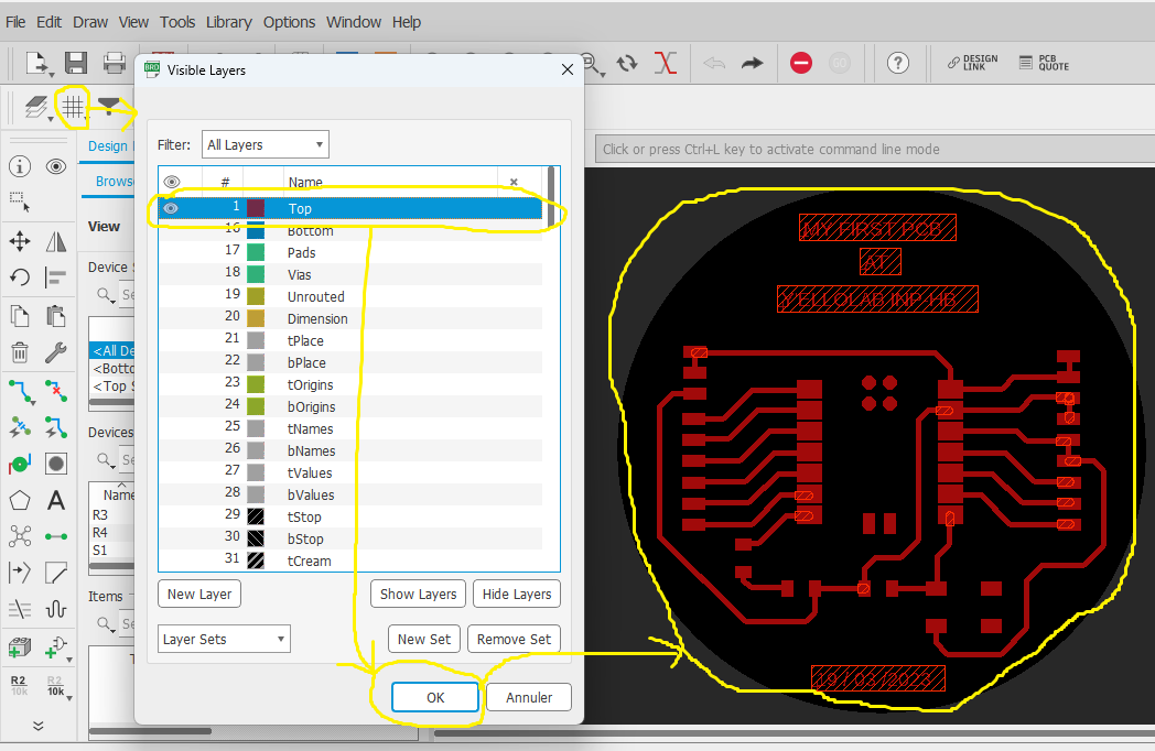
Generation of PNG files for the traces and the board outline
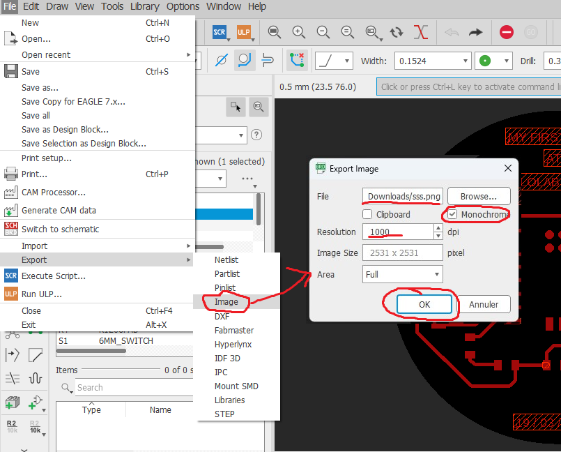
Once I have all the components placed and the tracks together, I need to export the file as a “.PNG”. But first we need to be only exported the tracks, and after the outlines. To do this we followed the process below:
- Click on “Layer Settings”, uncheck all but “Top” and click on “OK”.
- Go to File>Export and click on “Image” a window will open, click on “Browse…” to choose the file type and location, select “Monochrome” with Resolution = 1000 dpi and click on “OK”.
- Repeat the same procedure as above and in “layer settings” select “Dimension” instead of “Top”.
You should have the results below.