Electronics design
Individual Assignment
Hero Shot
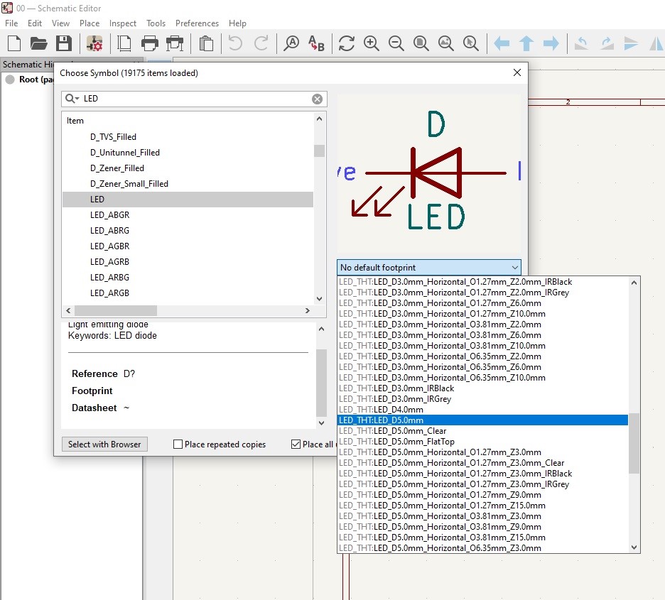
Using KiCad 7.0
I have Installed KiCad 07 and followed this tutorial to refresh my memory on it usage. Its a version 04 tutorial but it helps in getting started and understanding a minimum about PCB design workflow with KiCad (For me at least)
Summary
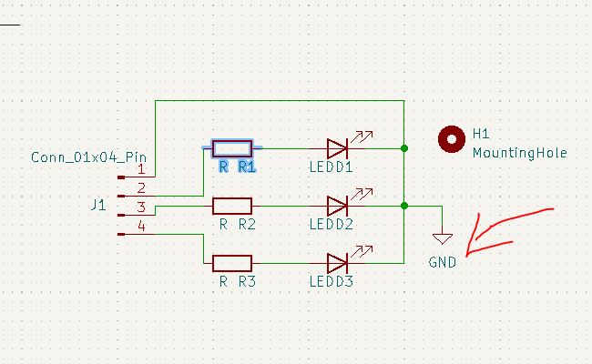
- Start with the Schematic tool to draw the PCB (Printed circuit board) schematic
- Add components symbols for the circuit (you can add the correct footprint here or add generic)
- Add wire connections
- Annotate the components and values
- Assign footprint to component if you didn’t add them with the components
- Add components symbols for the circuit (you can add the correct footprint here or add generic)
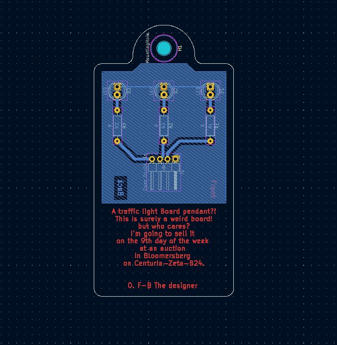
- Run Pcb Tool to trace/ design the physical board and position components properly
- Update PCB from Schematics
- Position the components,
- set component according to the face of the PCB they are positioned
- trace the copper traces with the trace tool (default shortcut “X” key) making sure it’s being traced on the right face (Front or back)
- add PCB outline to the edge cut layer
- Run design rule checker
- …
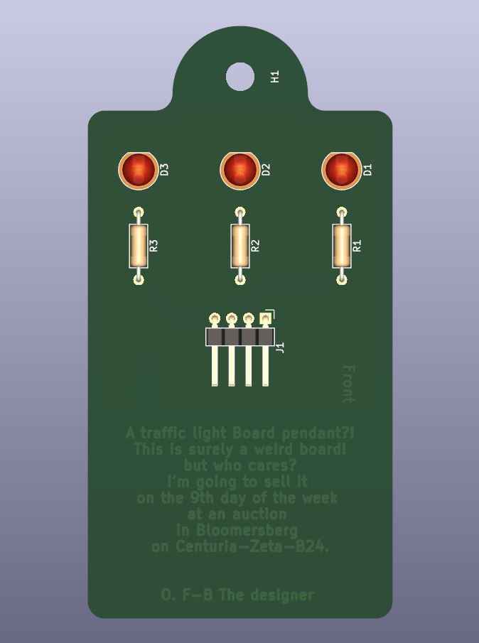
#### I tried to be serious on this one
Following the tutorial, I customized the board and added text labeling the front and the back. Added and Ground fill zone to it instead of connecting it with a wire trace. to do that you need to add a ground symbol and connect it to the circuit .ground.
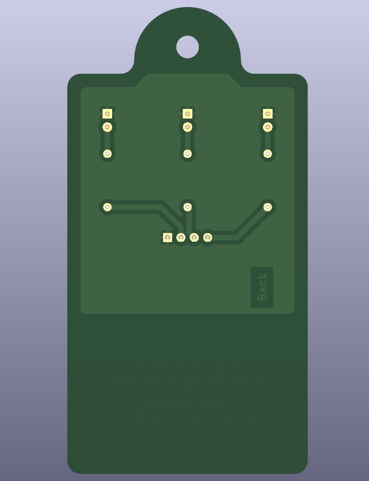
 I have also made sure my components were on the front and the traces on the back.
Front of the PCB
Back of the PCB
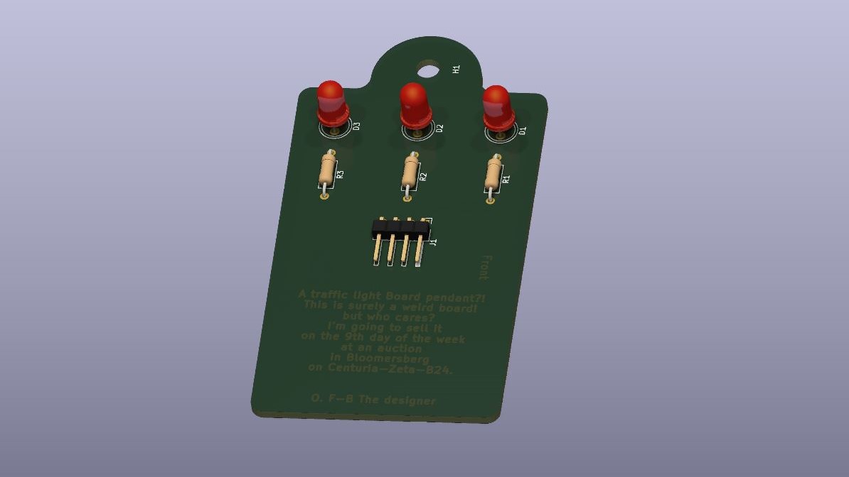
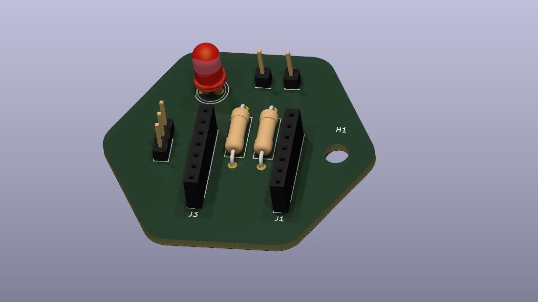
Designing a board for the Week 04 project
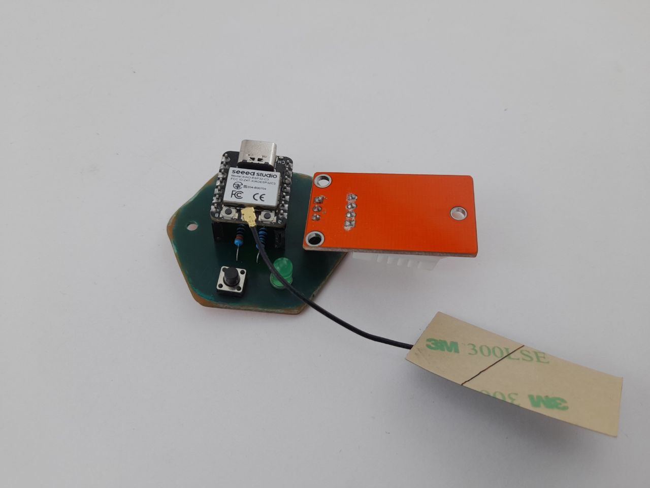
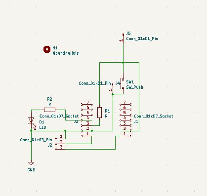
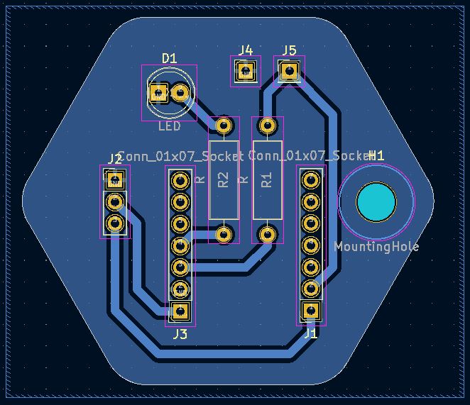
So on week04 I made a circuit with the XIAO-ESP32 so let’s design a proper board for it.
I have started with the schematics, the XIAO board will be fixed on 2.54mm pitch pin headers sockets.
I could find a footprint for my switch so I have added pin header with the same pitch.
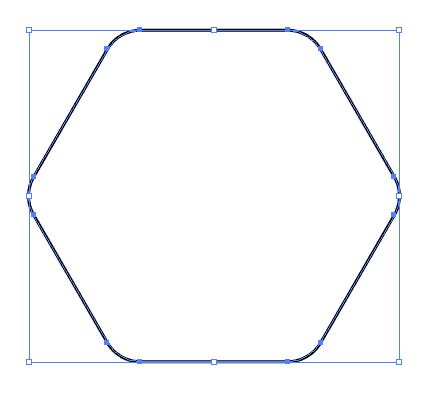
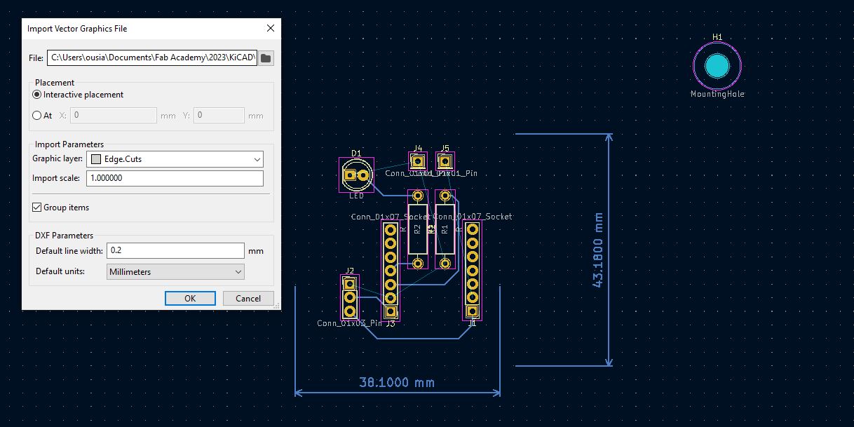
After that I opened the PCB design tool and imported an outline of a hexagonal vector for the PCB Shape.
I had to design it in Adobe Illustrator; and exported it as DXF. Then I imported it to the edge-cut layer. I have positioned the components traced the pad; ran design rule check and also checked the look from the 3D viewer
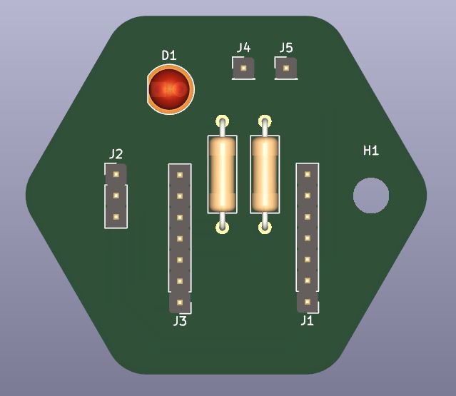
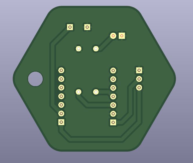
Result from the 3D viewer
Front
Back
Issues and troubleshooting
- As I wanted My components on the front and the cooper and soldering on the Back I forgot to mirror my design for the first milling. I have solved That by mirroring the imported Gerber file in flat cam before generating the geometry and exporting the CNC GCode.
- Due to uneven bed leveling or differences in copper board surface level (due to warping, particles on double-sided tape, etc…), it would be good to add a probe and do a grid Mesh leveling before every cut. This helps in making sure all the isolation routing comes out well.
Group Assignment
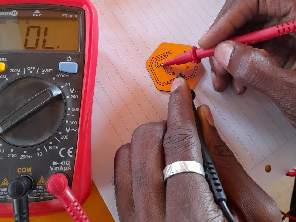
We have used the multimeter in its different mode: Voltmeter Amp-meter, and Continuity meter.
The continuity mode being used to check trace/pad isolation from each other.
We have also used the oscilloscope te measure output from XIAO board Blinking a LED. We have changed the ON/OFF delay to see the difference in reading.
Video of The oscilloscope With 1 second ON 1 second OFF delay
Video of The oscilloscope plot with 125 milli second ON 1 second OFF delay
Result
Picture of the Week 06 results
Pcb
Pcb render of my Design test Circuit
Pcb render of my Embedded Programming week project with XIAO-ESP32
File
Test Circuit Design - Ki Cad Pro Schematic & PCB Week04 Circuit Design - Ki Cad Pro Schematic & PCB