Electronics Production
Task for the week
Group assignment:
- Characterize the design rules for your in-house PCB production process: document feeds, speeds, plunge rate, depth of cut (traces and outline) and tooling.
- Document your work to the group work page and reflect on your individual page what you learned
Individual assignment:
- Make and test the development board that you designed to interact and communicate with an embedded microcontroller.
Foreword
As I watched the small CNC machine in action, I was in awe of the sheer genius behind its design. It was as if I was witnessing the evolution of technology unfolding right before my very eyes. My passion for machinery and the ability to bring ideas to life only grew stronger with each passing moment.
Despite my enthusiasm, the week was not without its challenges. I had to make some modifications to my PCB design and my introduction to CNC machining began with the unfortunate incident of breaking a mill while attempting to determine the zero point on the surface.
But such is the nature of any new adventure, and I am excited for what lies ahead. With each passing day, I am one step closer to holding in my hands the very first board I have created on my own.
Group Assignment
As we began the group assessment, we had the opportunity to become familiar with the Roland CNC machine and the variety of mills used in our work. Once the machine was prepped and ready, we proceeded to download .png files and put our skills to the test. Utilizing the Mods, we generated the necessary g-code to execute the milling process. Our initial test involved using a 0.5mm bit to determine how many gaps it could handle. For the actual cutting of the board, we switched to a 1/32 inches mill, which allowed for a more precise and accurate cut. The entire process was a true testament to the power and versatility of modern technology and the endless possibilities it presents.
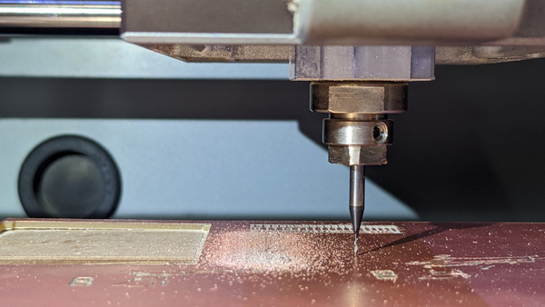

For this test with the 0.5mm mill, it was only able to carve inside the 0.020 inch gap. Which is coherent, because 0.020 inch is equal 0.508 and 0.019 inch is equal to 0.4826mm.
Afterwards, we tried with a 0.1mm v-shaped bit:
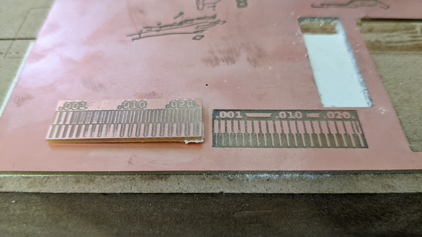
It became obvious to me how the “invert” function works. I was also surprised by the fact that despite the fact that mill was v-shaped, it still managed to passe more distance.
You can find more details and observations in the Group Assignmet page.
My first PCB ever!!
Before delving into the Mods and tools I used to create my board, I feel it’s important to share a little hiccup I encountered during the process. As I was setting up the work surface for milling on the CNC, I unfortunately managed to break a mill. This happened when I failed to correctly adjust the Z-axis setup and accidentally lowered the drill lower than necessary. When I lifted the drill back up, I was dismayed to find that the sharp head of the mill was still sticking out of the worktop surface. While frustrating at the time, this experience taught me the importance of precision and attention to detail when working with such delicate tools and machinery.
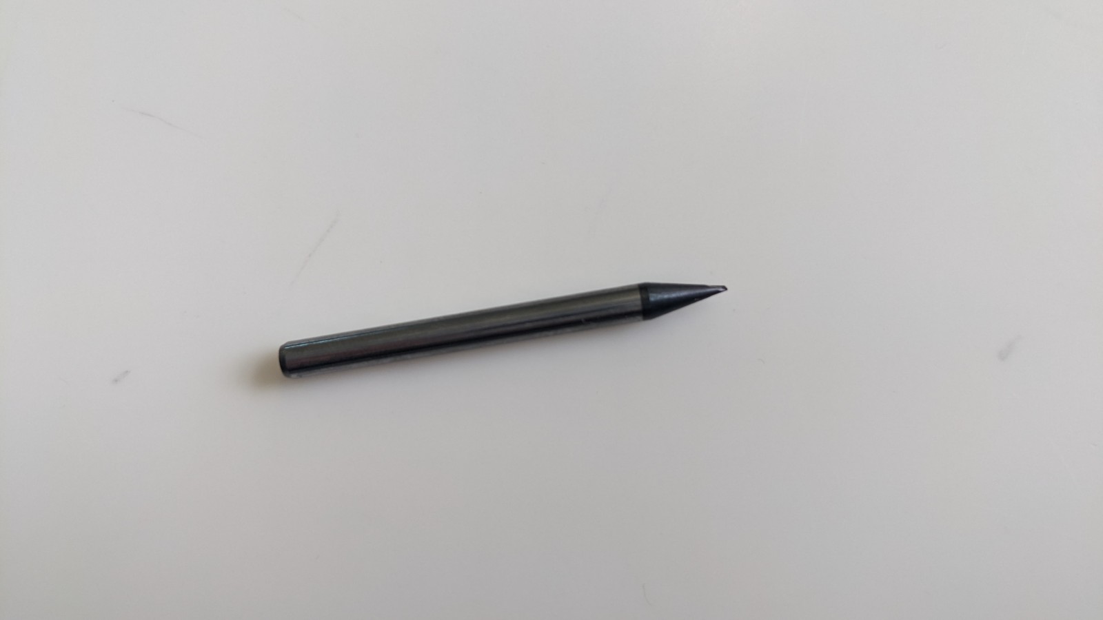
I kept this mill as a keepsake!
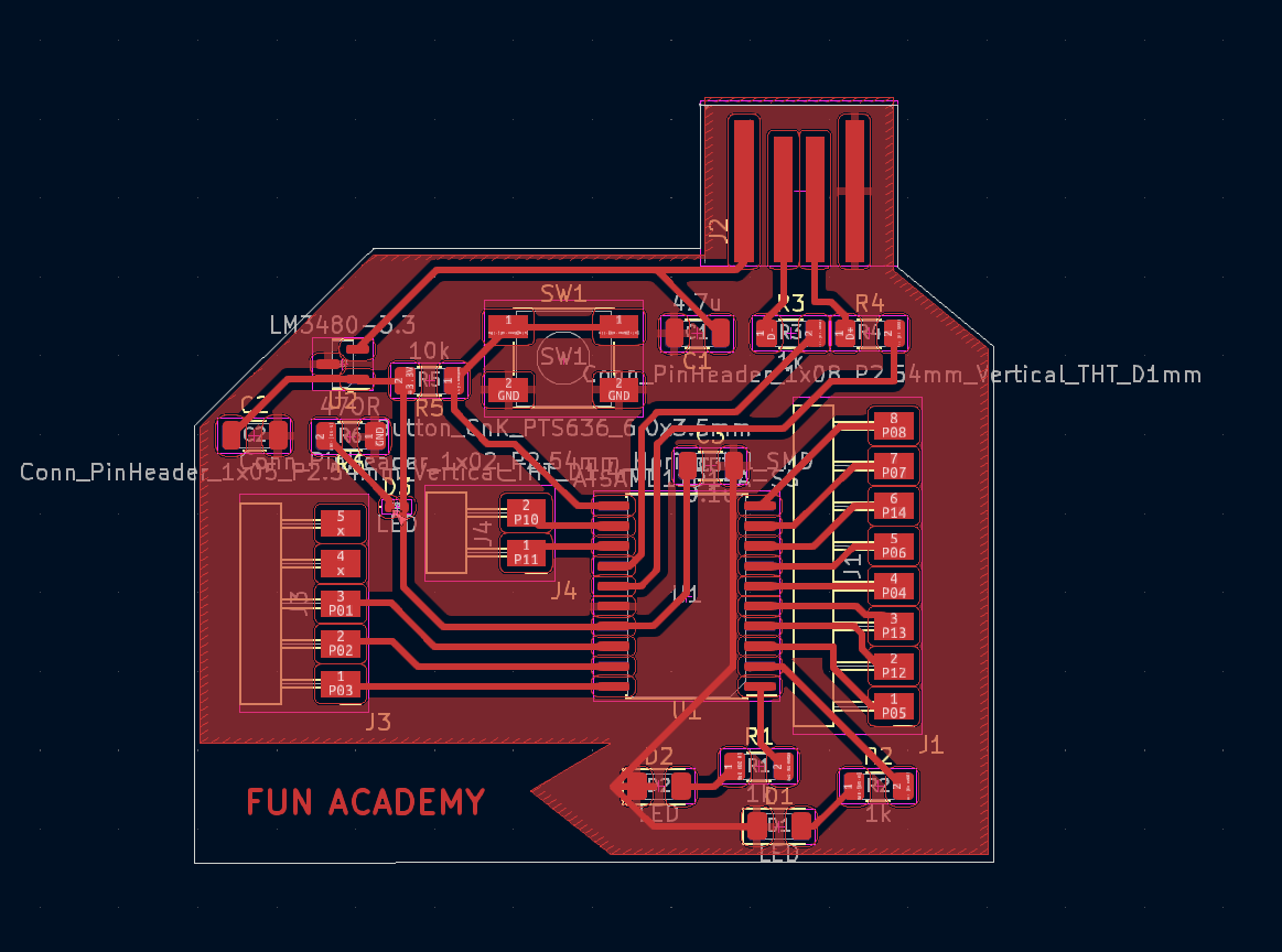
New shape for PCB
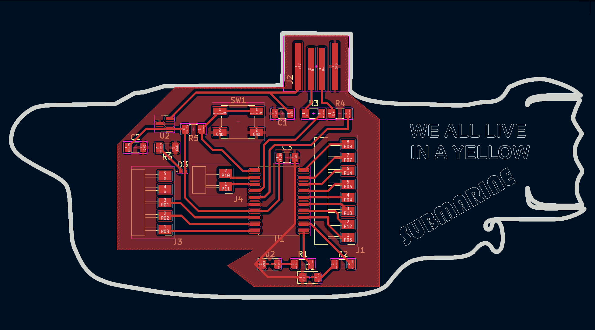
When it came time to create a real board, I realized that in fact the tail of my “submarine” could interfere with USB. And I had to come up with a new shape for my board.
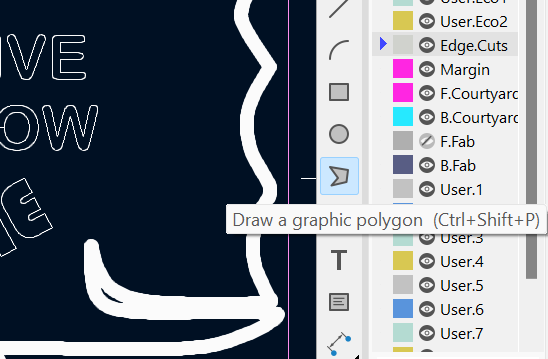
Now I need to delete my pretty shape and use the appropriate tool from the toolbar to draw a new cut edge.
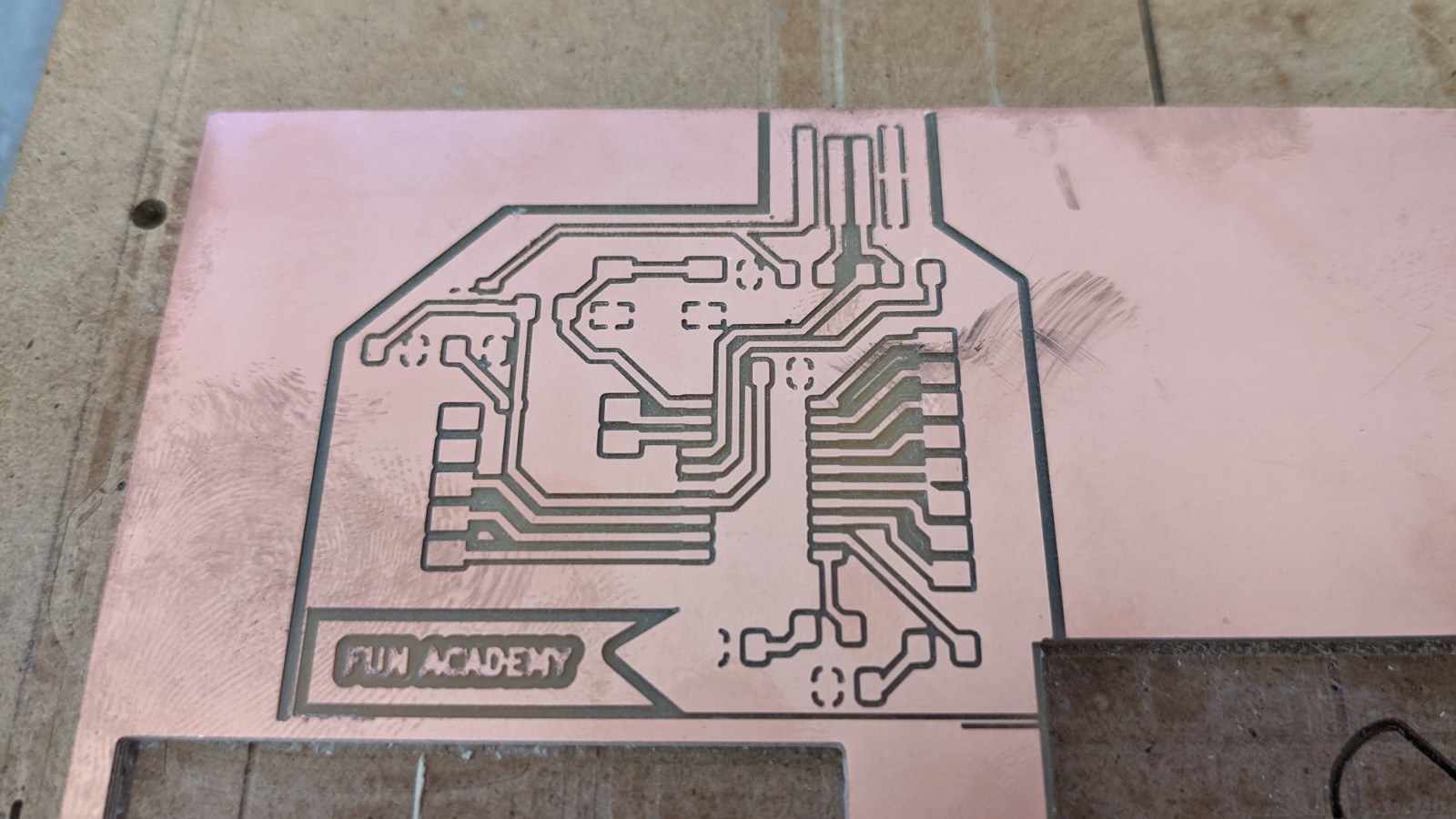
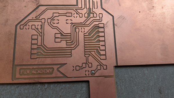
I decided to write Fan Academy on the board, because since the beginning of Fab Academy, every day has been hard fun for me.
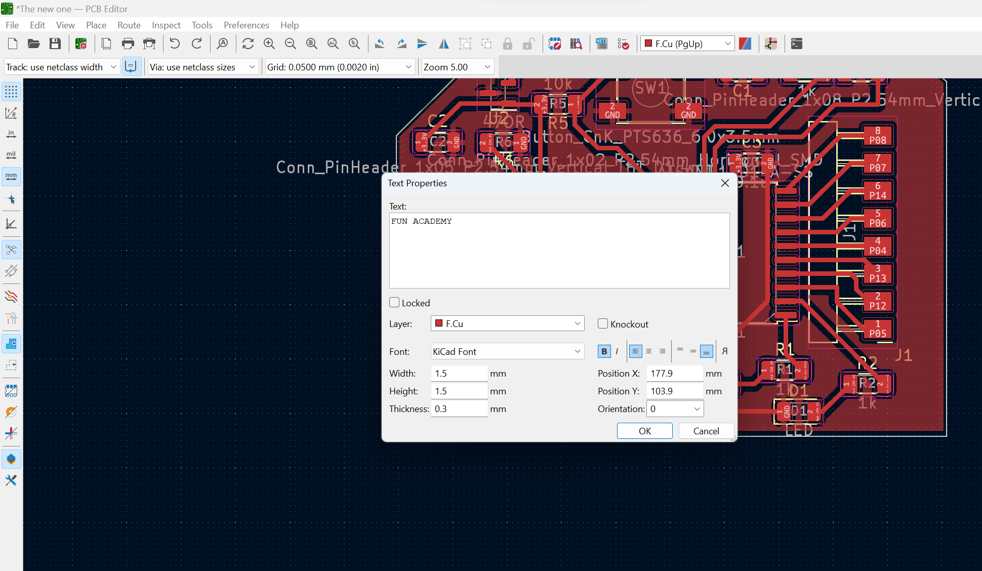
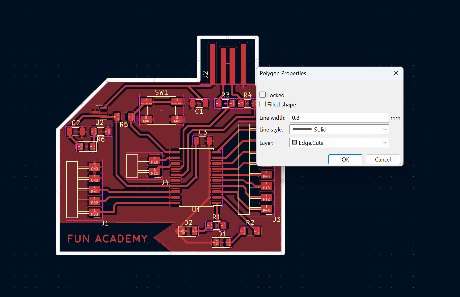
To cut my PCB, I will be using a 0.8mm mill. It’s important to ensure that the edge cut also has a thickness of 0.8mm. To achieve this, simply right-click on the line and select “Properties”. In the resulting window, you will be able to adjust the line thickness to the desired setting.
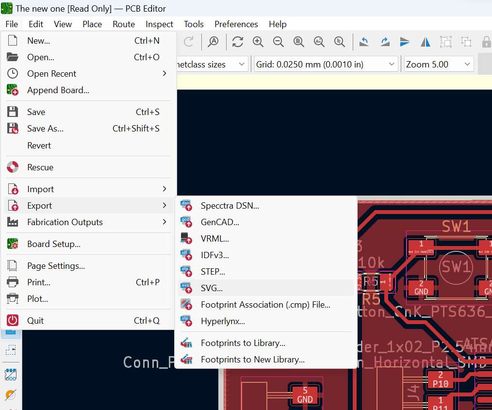
For Export the files on .svg format: Files -> Export -> SVG
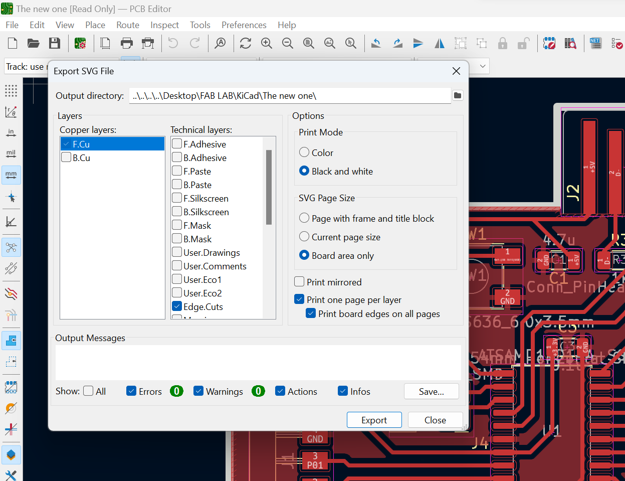
Here I chose Front Cut from Copper Layers and Edge Cuts from Technical Layers:
G-code
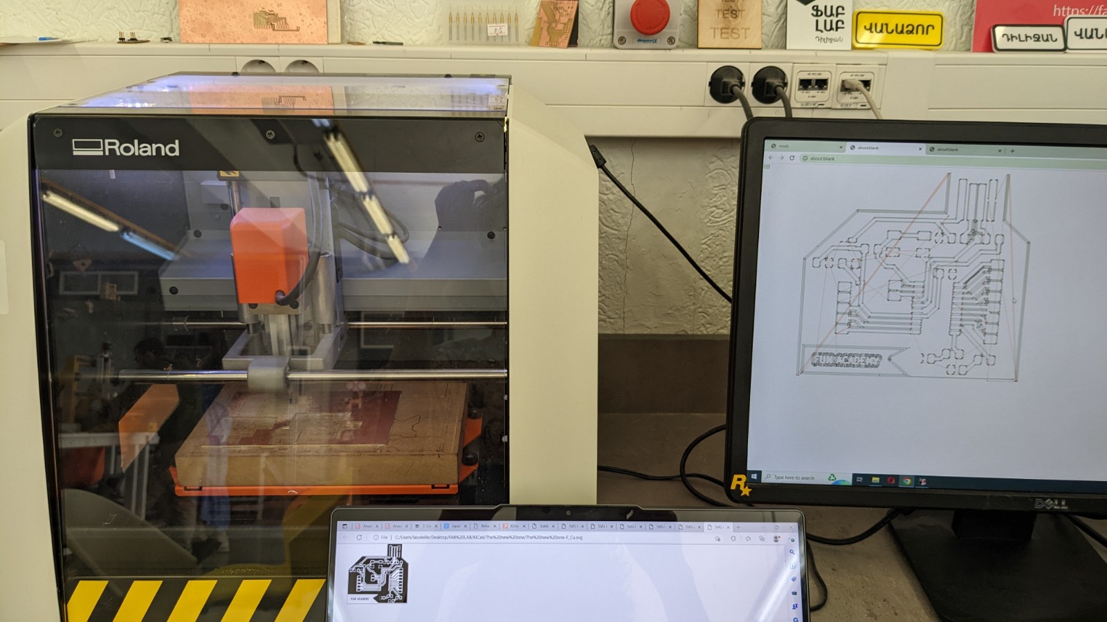
Now, in order for the C&C machine to understand our commands, we need to generate a G code. https://mods.cba.mit.edu/ is a simple tool we can use.
Now right click and follow the steps:
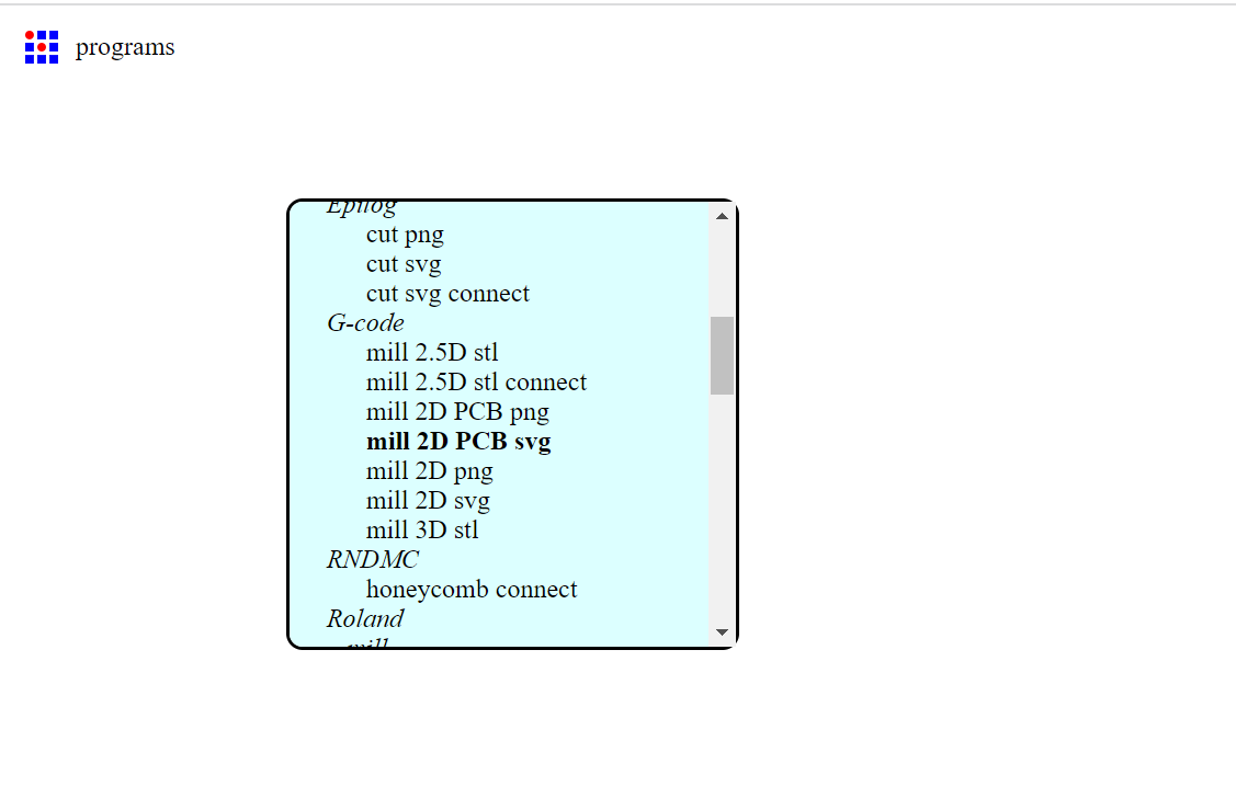
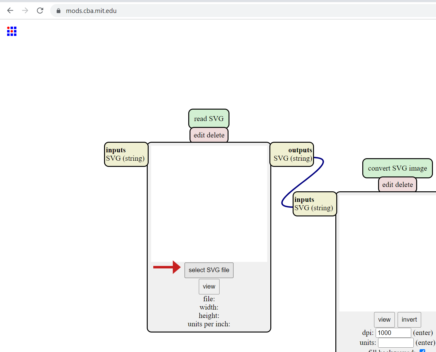
Here we need to find the .svg file of our PCB.
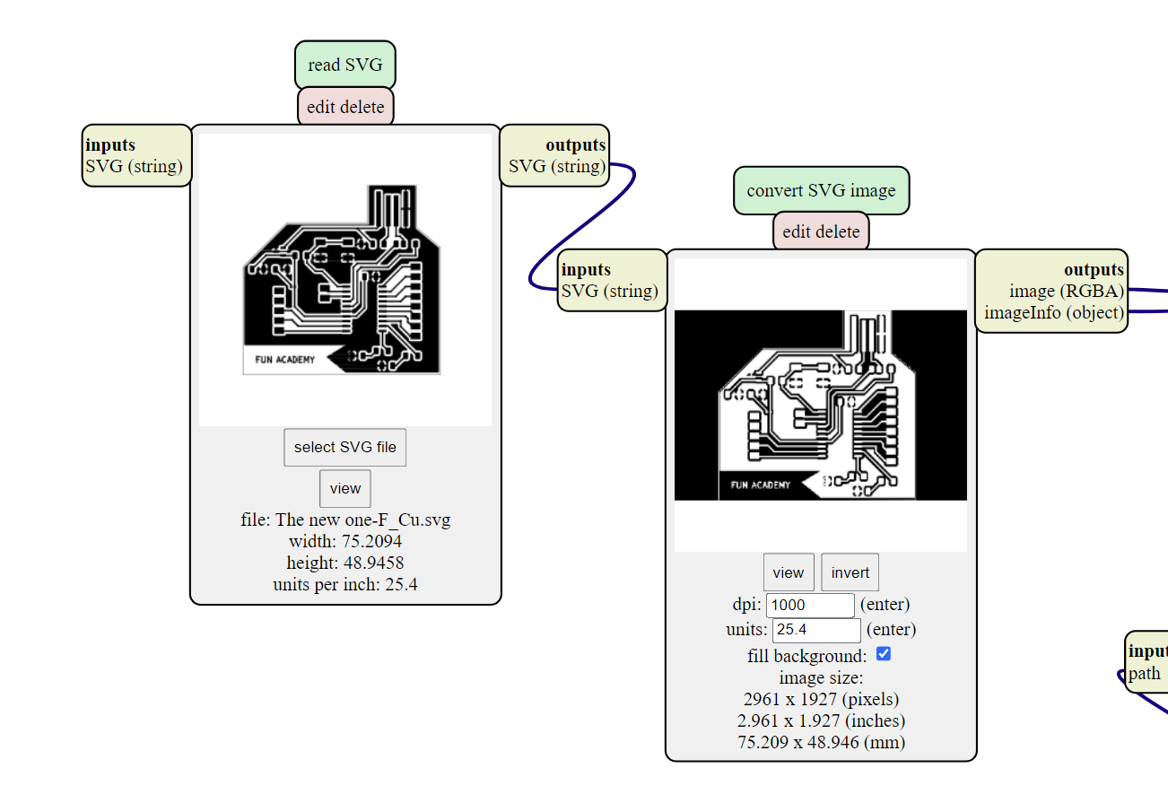
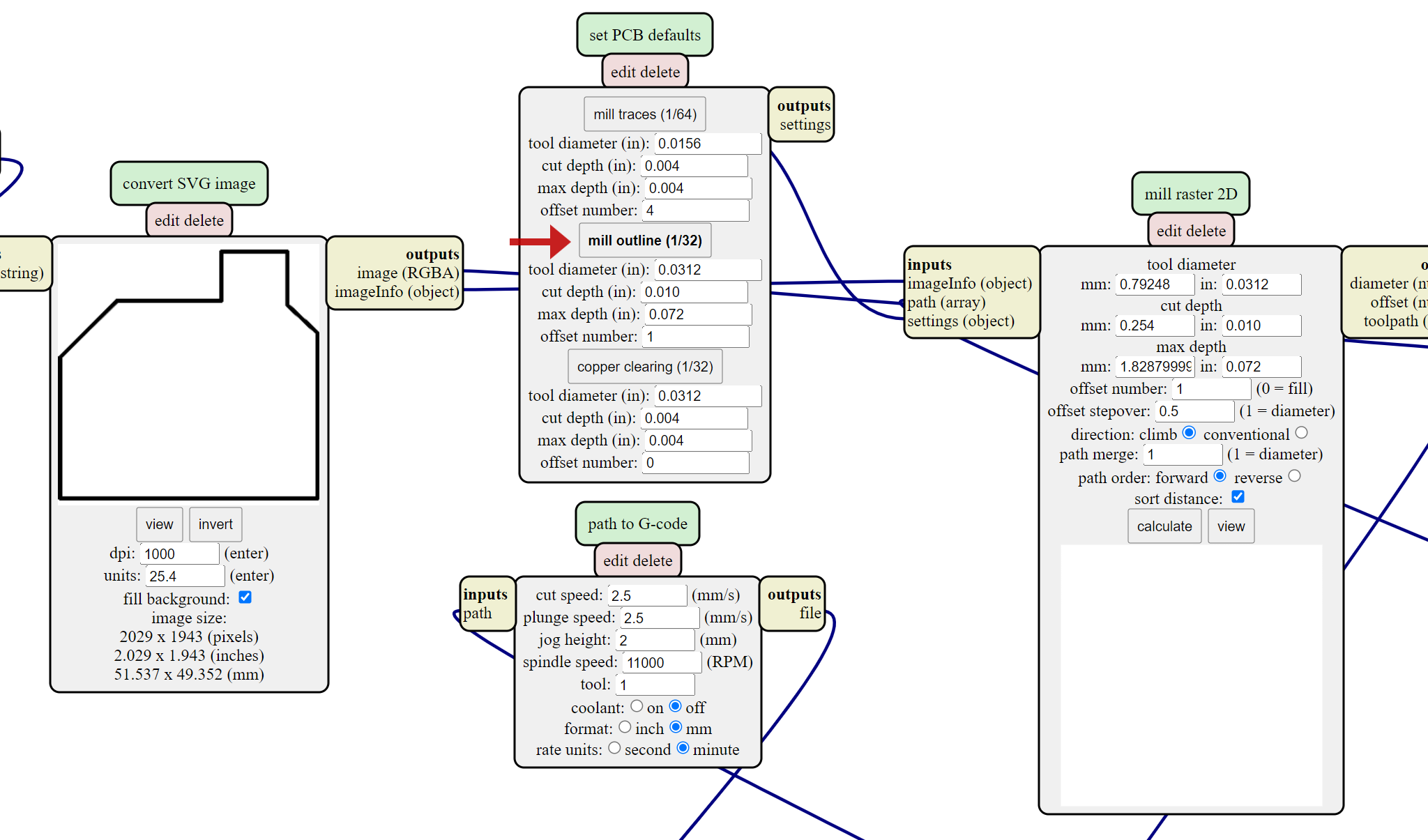
In the second window we invert the drawing to have the right milling. We can chose the size of the mill and select Calculate
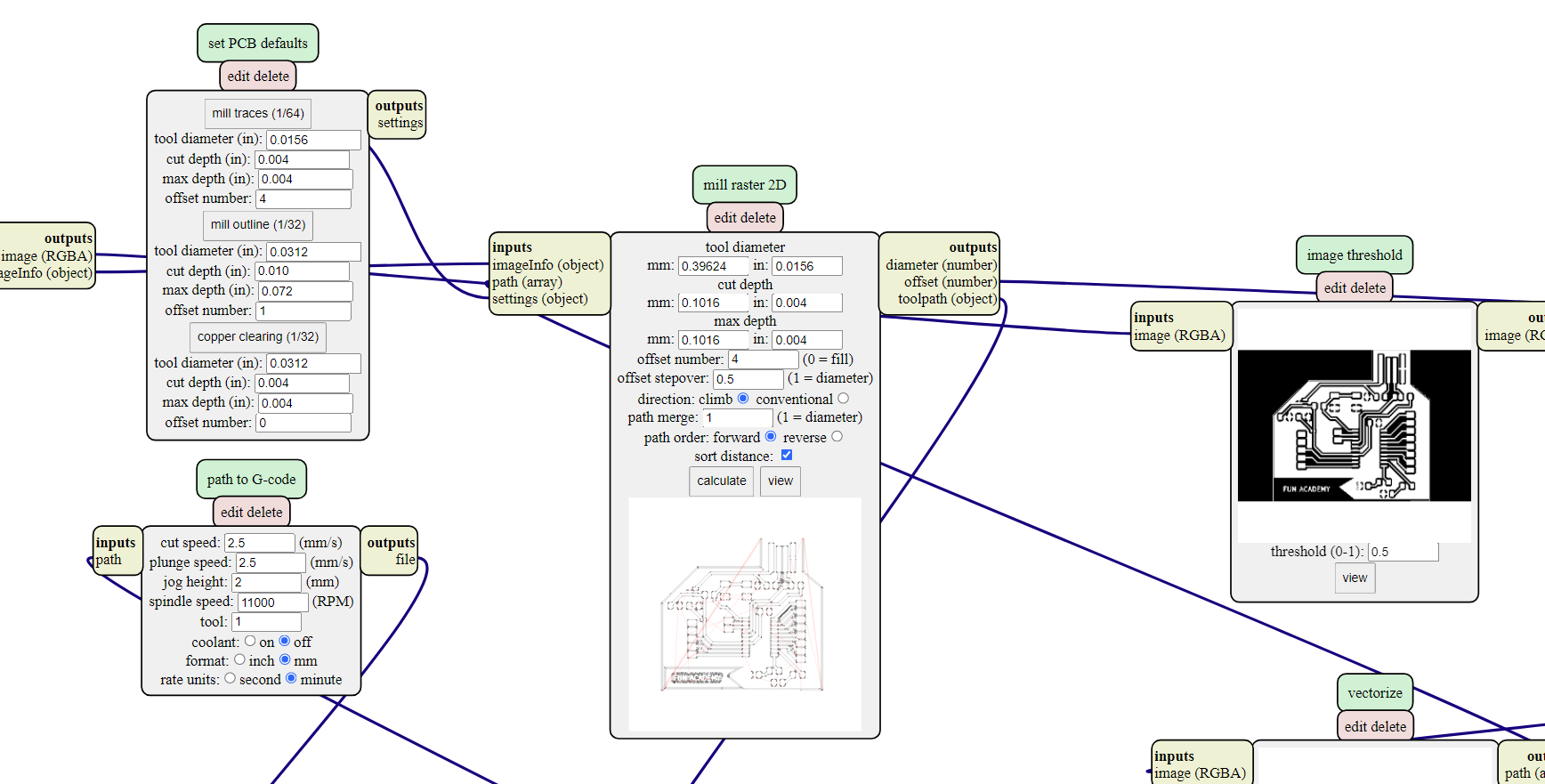
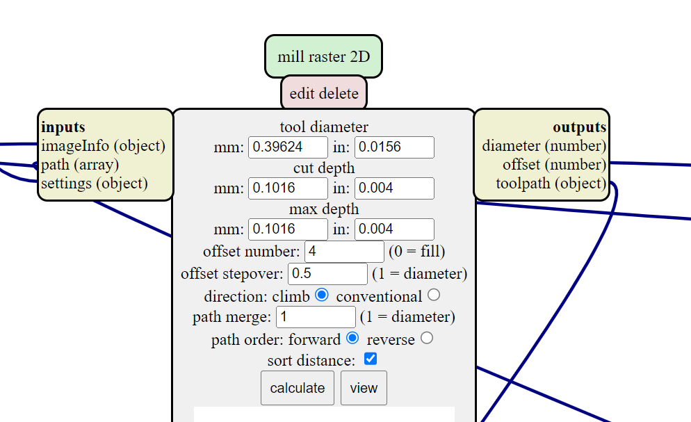
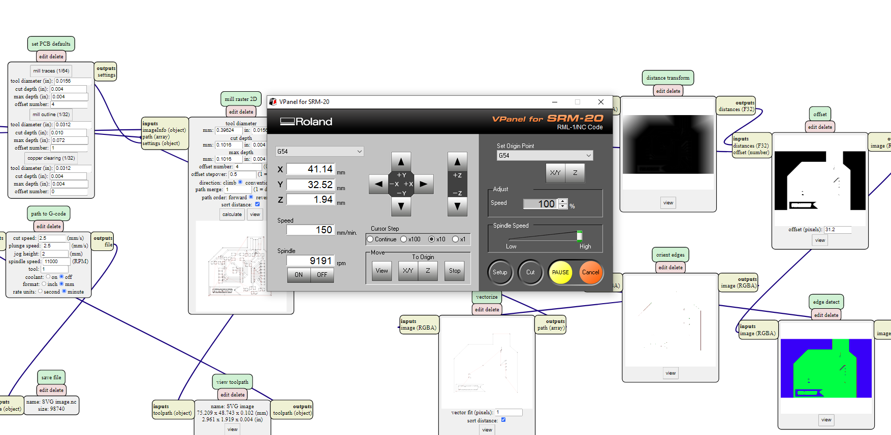
Mods Parameters
In mods we see few parameters to set up: in this window we have 3 options
- mill traces
This option refers to the process of milling or cutting the copper traces on a PCB. Traces are conductive pathways that connect different components and elements on the PCB. When you select the “mill traces” option in the software, it generates G-code instructions to guide the milling machine in cutting the copper traces according to the design specifications.
- mill outline
The “mill outline” option involves milling or cutting the outer perimeter or outline of the PCB. This operation shapes the PCB board to its desired dimensions and removes any excess or unwanted material. The mill outline process ensures that the final PCB has the correct size and shape according to the design requirements.
- copper clearing
Copper Clearing: Copper clearing, also known as copper removal or copper isolation, is the process of milling or cutting away unwanted copper areas on the PCB. This option is used when you want to remove excess copper from the board, such as areas not covered by traces or copper pour planes. Copper clearing helps create insulation between different traces or components, preventing unintended electrical connections or short circuits.
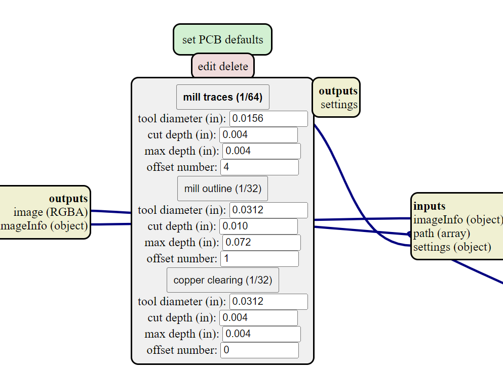
Depending on the selected option, the next window will present the setup for the specific task. We can customize it based on our design and tools.
Some important parameters here:
- Tool Diameter: This refers to the diameter of the milling or drilling tool used to create traces, holes, or cutouts on the PCB.
- Cut Depth: The cut depth specifies how deep the milling tool should penetrate the PCB material when cutting traces or creating cutouts. It is usually defined in terms of a specific depth value or as a percentage of the PCB thickness.
- Max Depth: The maximum depth parameter sets the maximum depth that the milling tool can reach during the cutting operation.
- Offset Number: In PCB milling, an offset refers to creating multiple passes around a trace or cutout with progressively increasing or decreasing distances from the original path. The offset number determines the number of offset passes to be performed.
- Offset Stepover: The offset stepover parameter determines the distance between adjacent offset passes when using offset milling. It specifies how much the tool should move between each pass.
Milling
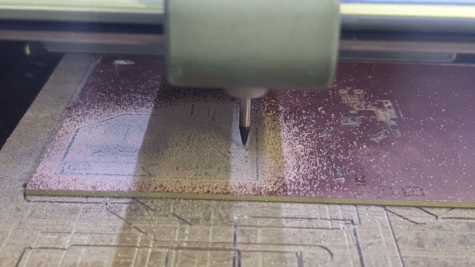
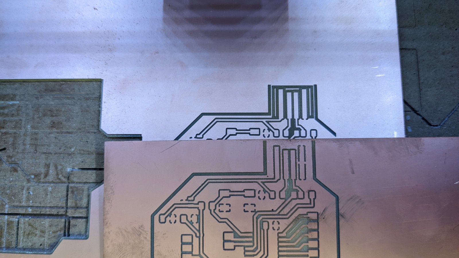
Now it’s time to use G code and start milling. We open VPanel for SRM-20. Here we setup the axis finding the starting point on X, Y and Z.
I press the Cut button, load our file with the G code and enjoy the spectacle of how CNC performs its work beautifully.
Following the milling process, I observed an issue with the USB component of my PCB design. Seeking a solution, I consulted with fellow students in our lab, who recommended removing the fillings from the USB part. Although this meant making changes to my design once again, I was grateful for the opportunity to learn from my mistake and collaborate with my peers.
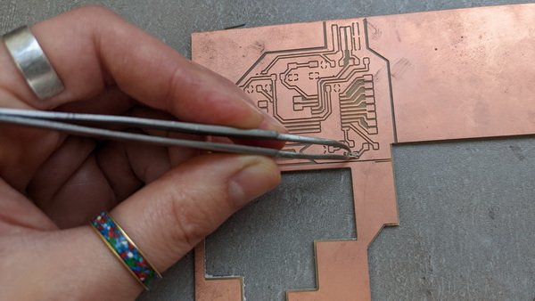
Following the removal of the fillings, I proceeded to repeat the milling process. Can you spot the difference? With the milling now complete, it’s time to cut my board and begin the soldering phase. I’m excited to see my design come to life and put my skills into practice.
To move on to cutting, we need to repeat the steps in Mods in the same way as shown earlier with milling. The only difference is that in the third window we need to select mill outline:
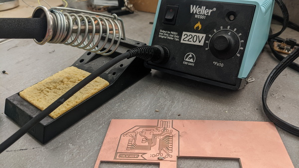
In the meantime, while the machine was cutting my PCB, I was practicing soldering on the failed board.
Time for miracles and a new PCB
Soldering
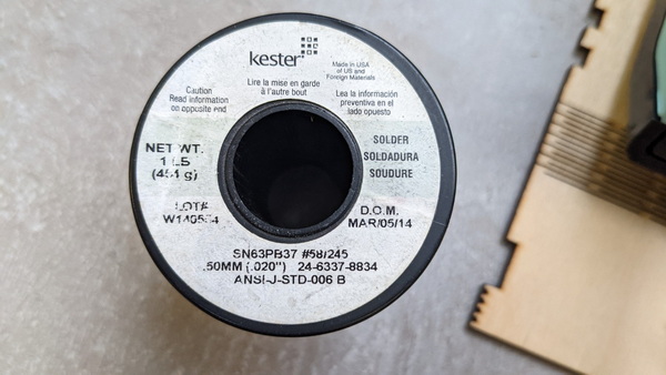
What you need is Soldering Iron, Solder, Тweezers and a wet-wet sponge!!
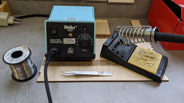
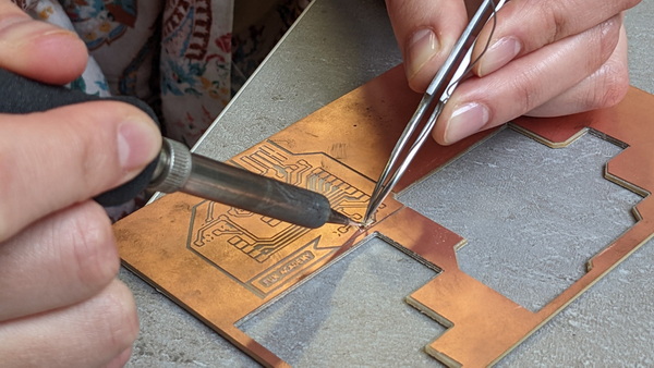
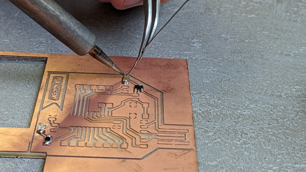
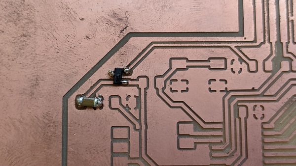
As I mentioned, I started practicing soldering on my failed board with reused components, and now I’ve entered the incredible world of soldering. I began by heating the soldering iron and wetting the sponge, which is an essential step in cleaning the nozzle of the iron. Taking a piece of solder, I melted it slightly and placed a dot on the designated spot for an LED.
Using tweezers, I picked up the LED and soldered one side. Then, I added more solder to ensure a strong connection with the board. It was my first experience, and I felt ecstatic! It’s important to frequently clean the nozzle to prevent any unwanted residue on the board.
Moving on to the next component, which was a resistor, I repeated the same process. The most challenging part was soldering the voltage regulator, which had “short legs,” as well as the capacitor that required more solder and precision.
Despite feeling tired, I was thrilled with this newfound skill.
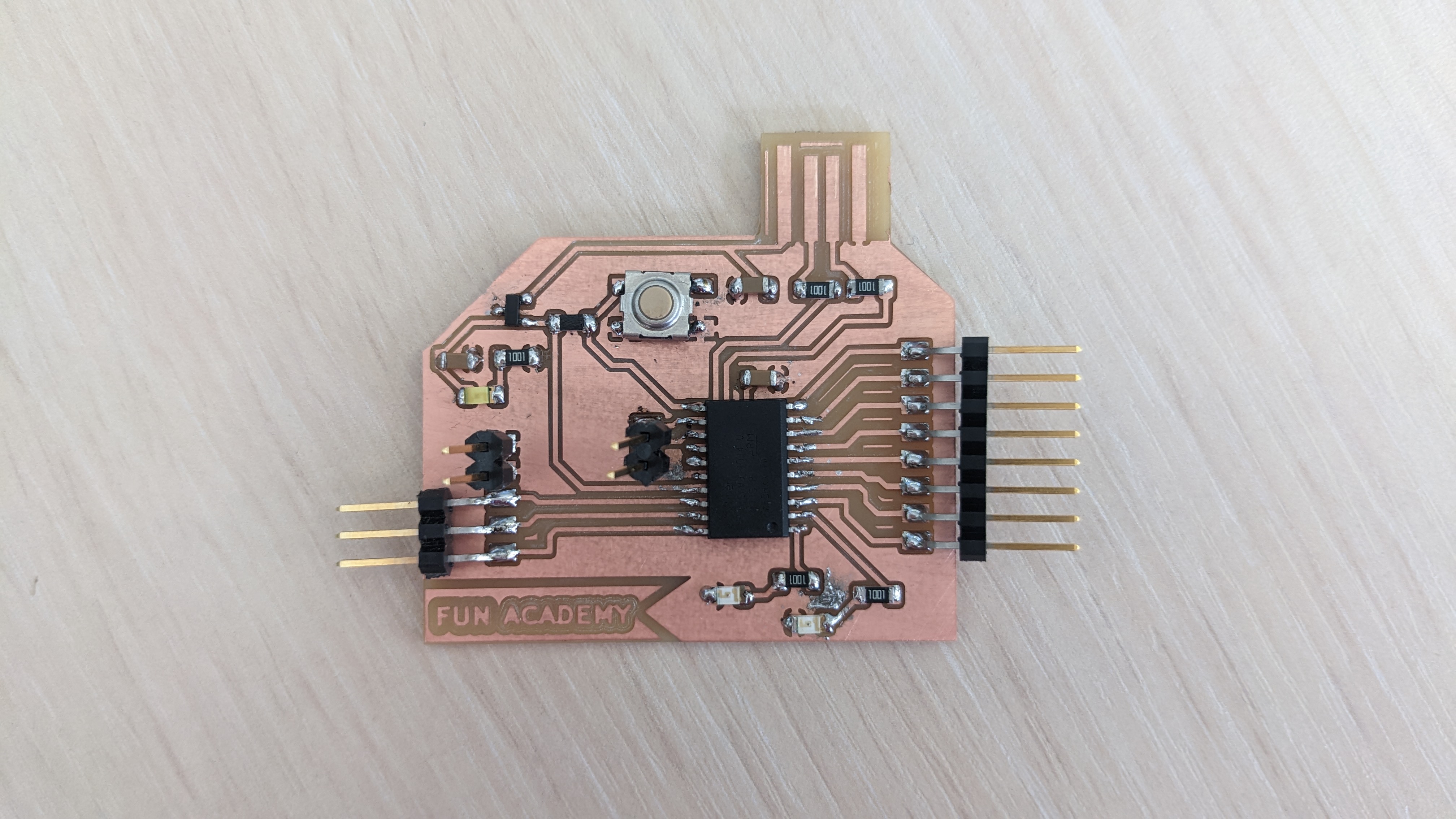
Components on my PCB
| Qty | Component |
|---|---|
| 1 | Microcontroller |
| 1 | Voltage regulator |
| 1 | Switch button |
| 6 | Voltage regulator |
| 3 | Capacitors |
| 3 | LED |
| 1 | USB |
| 2,5,8 | Pin Connector |
- Microcontroller ATSAMD11D 14-U: The central processing unit responsible for executing programmed instructions and controlling the functions of the PCB.
- Voltage regulator: A component that converts the input voltage of 5V to a regulated output voltage of 3.3V, ensuring a stable power supply for other components.
- Switch button: An input device used to initiate specific actions or control functions on the PCB when pressed or toggled.
- Resistors: Passive electrical components that limit or control the flow of current in a circuit, used for adjusting voltage levels or setting current values.
- Capacitors: Passive electronic components that store and release electrical energy, used for filtering, decoupling, or smoothing voltage levels.
- LEDs: Light-emitting diodes that emit light when an electric current passes through them, used for visual indicators or displays.
- USB: Universal Serial Bus interface for connecting the PCB to external devices or power sources, allowing data transfer or charging.
- Pin connectors: Connectors used to establish secure electrical connections between the PCB and external devices, facilitating easy connection and disconnection.
The new PCB
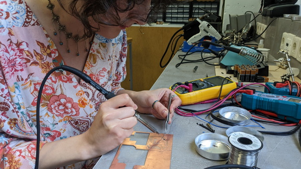
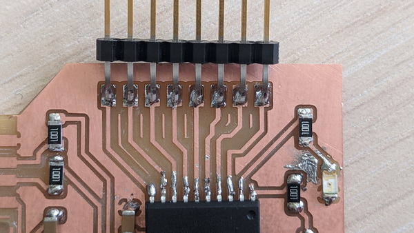
With the PCB now milled and ready for assembly, I dive into the intricate process of soldering the various components onto the board. Carefully placing each component onto the board and then soldering them onto their respective pads using a soldering iron, I refer to the PCB design and schematic to ensure that each element is placed and soldered accurately. Although a time-consuming task, the sense of purpose and accomplishment it brings is undeniable.
While watching informative videos like the one I found at this link can be helpful in understanding the basics of soldering, nothing beats hands-on practice. The more I work with my own PCBs and components, the more comfortable and confident I become with my soldering techniques. So, while the theoretical knowledge is essential, it is ultimately the practical experience that will help me master the art of soldering.
As I soldered the first LED, I couldn’t resist the urge to test the circuit and ensure everything was working as intended. In the following two photos, you can see the difference: the first photo shows the LED illuminated as a result of the contact.
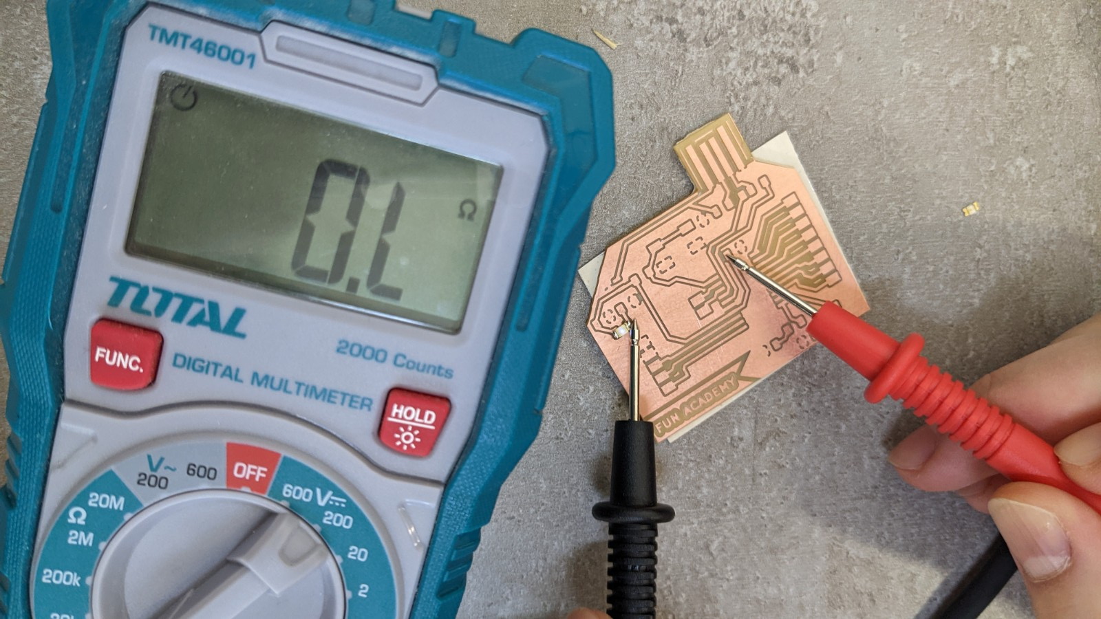
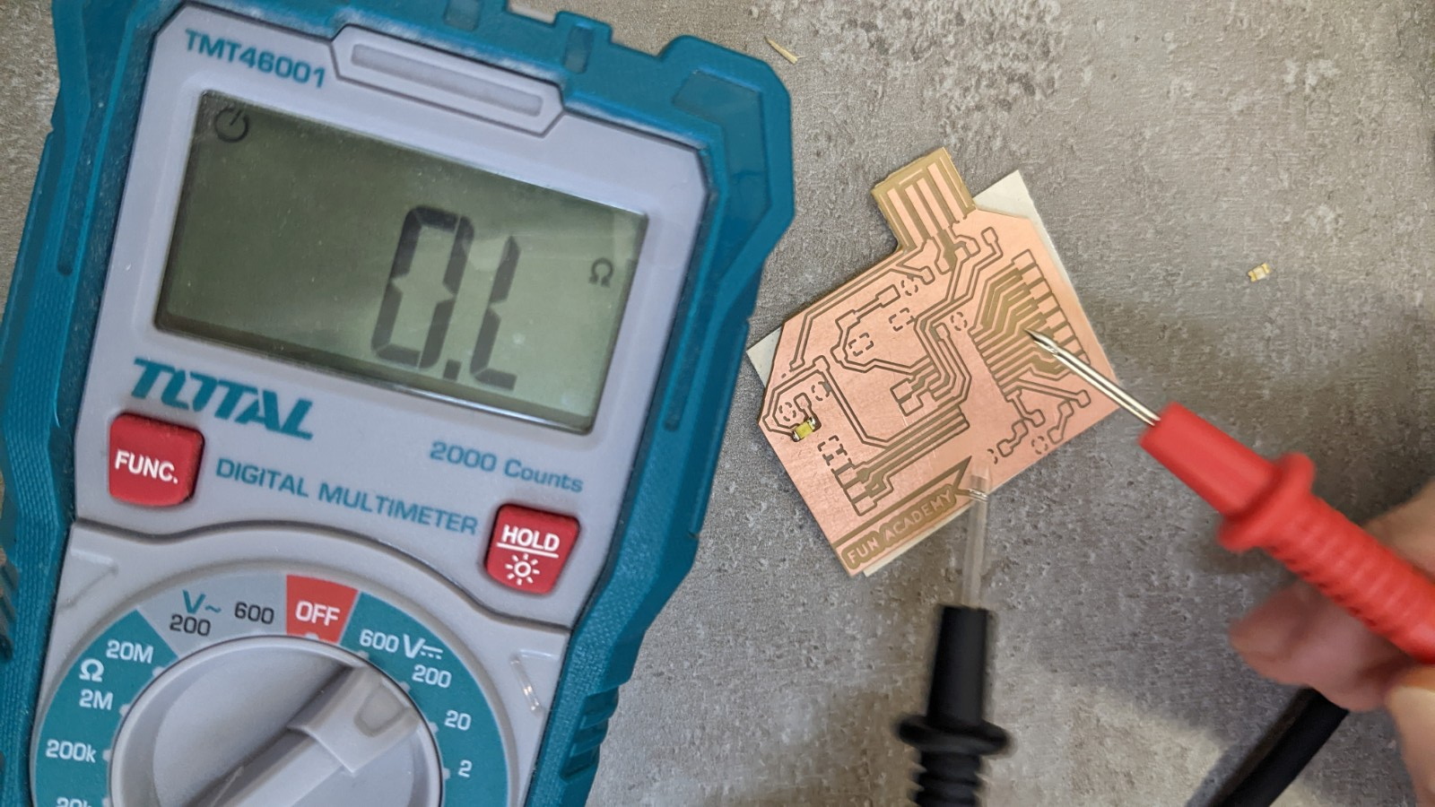
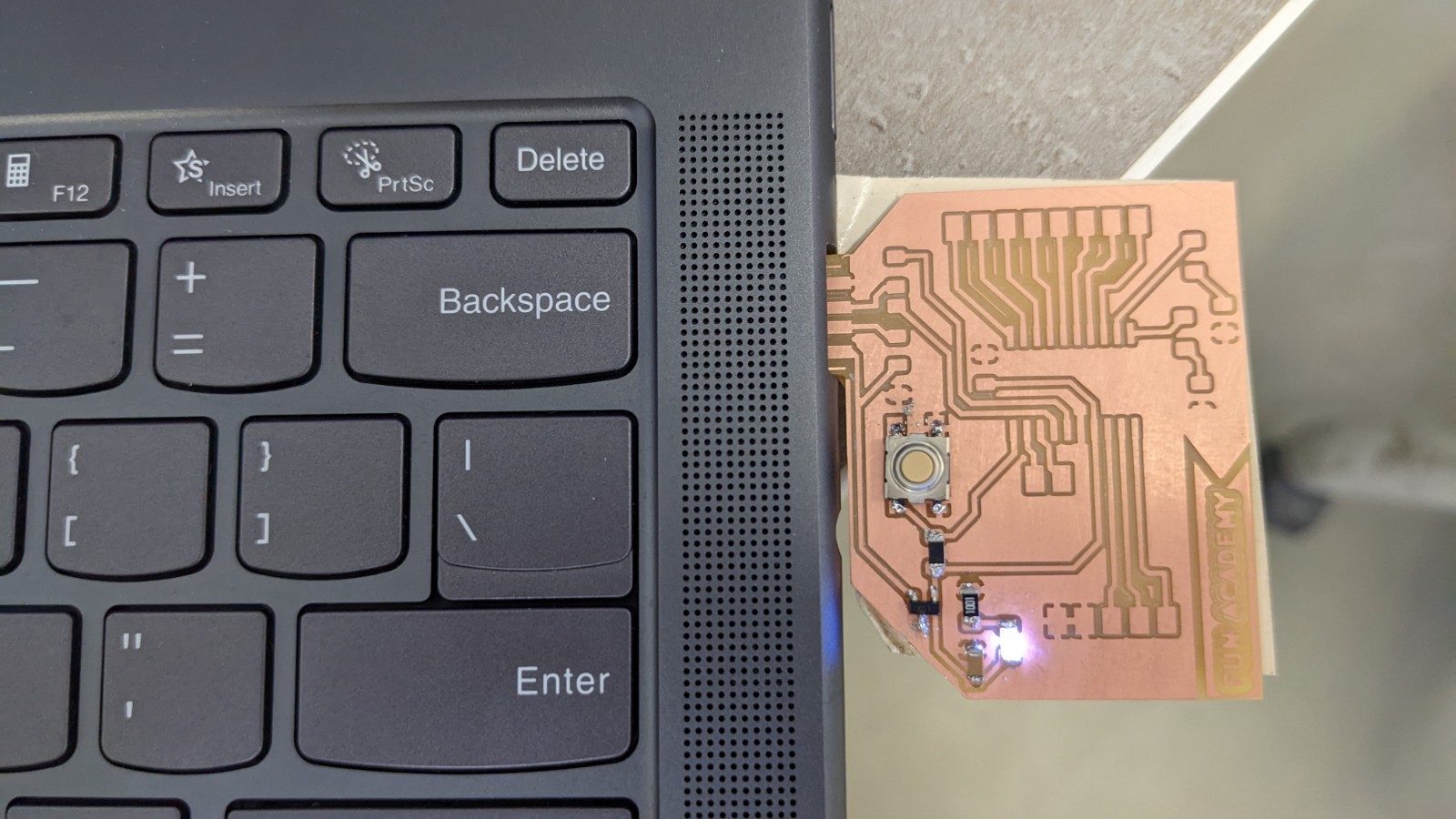
After soldering several components, I couldn’t resist the urge to see the fruits of my labor. Excitedly, I connected the board to my computer (although I knew it wasn’t safe to do so just yet). I admit, I have little patience when it comes to these things. As I watched with bated breath, my heart leapt with joy as the power light illuminated. In that moment, I felt like the happiest person in the world, proud of my hard work and eager to continue on my path towards mastering the art of PCB fabrication.
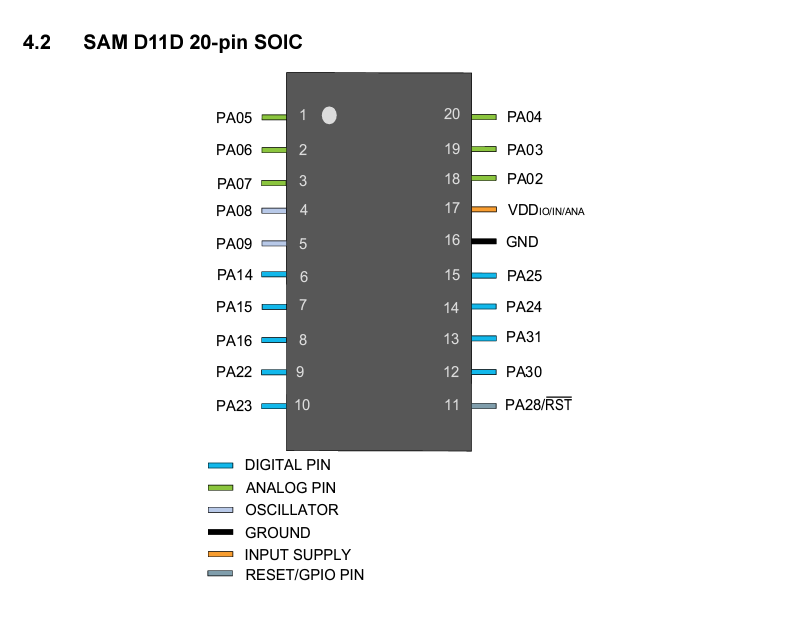
The next challenge was met with elegance as I approached the task of soldering the microcontroller. At first glance, the black rectangle seemed identical on both sides, leaving me puzzled as to which direction to proceed. However, a cleverly placed hole served as a guide, revealing the proper orientation of the SAMD11D microcontroller’s pinouts as outlined in the informative [datasheet] (chrome-extension://efaidnbmnnnibpcajpcglclefindmkaj/https://ww1.microchip.com/downloads/en/DeviceDoc/Atmel-42363-SAM-D11_Summary.pdf). With a newfound understanding, I confidently soldered the microcontroller in the correct direction, bringing me one step closer to my finished project.
Finally, after carefully placing all of the components in their designated spots, I stepped back and marveled at the beauty of imperfection. Despite the messy soldering job, I was filled with a sense of happiness knowing that I had successfully created something incredible for myself. As I looked at the perfectly functioning PCB board, I couldn’t help but apologize for the untidy soldering. But then again, it was my first time and I learned that even in the face of imperfection, the beauty of accomplishment is always present.
Hero shot
In conclusion, while I wasn’t able to program my PCB this week, I am proud of my accomplishments and look forward to continuing my exploration of the documentation in the coming weeks. Each week of Fab Academy brings new challenges and opportunities for growth, and I am grateful for the chance to feel like a Super Woman as I tackle them head-on. Thank you for sharing in my success, and here’s to the exciting adventures that lie ahead.
Programming (from Output Devicesweek)
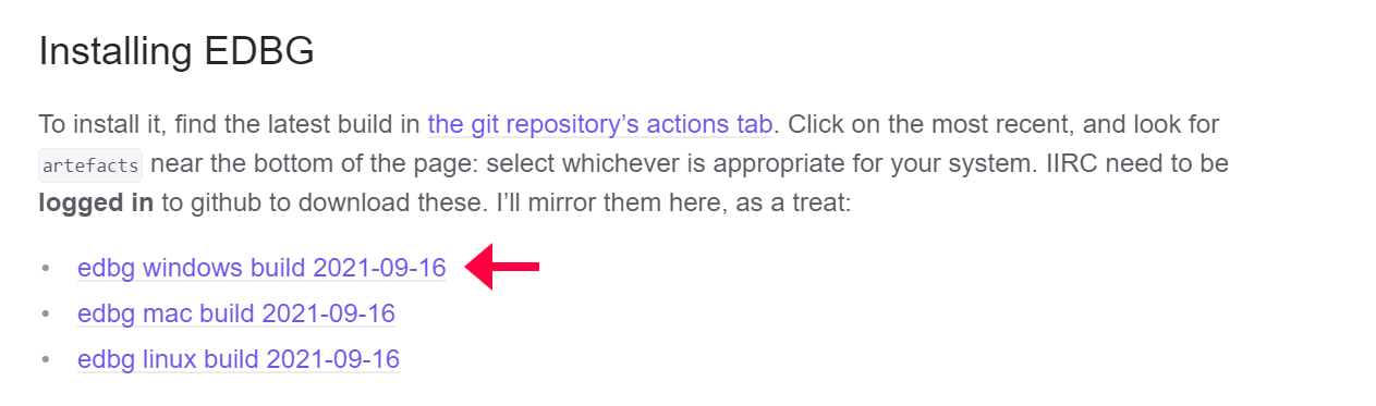
EDGB install
To load the bootloader into the board, we need to install The Atmel® Embedded Debugger (EDBG) - an onboard debugger for integration into development kits with Atmel MCUs. “In addition to programming and debugging support through Atmel Studio, the EDBG offers data streaming capabilities between the host computer and the target MCU.” You can find out more about EDBG here
To install EDGB, I selected the relevant link from the EDGB guide page. Since the operating system on my computer is Windows, I chose the following link.
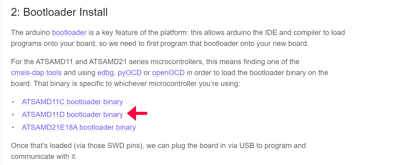
Bootloader install
Now we need to install the bootloader. I found the description and the .bin file I need in Fab Arduino SAM Guide
(There I also found details on how to set up Arduino in order to write code for my own board. But more on that later.)
Here I have selected the option that is intended for my board with microcontroller ATSAMD11D14A-SS.
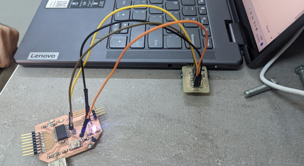
Now we need to collect edgb.exe and sam_ba_SAMD11D14AS.bin them in one folder. Here we run the GitBash. Writing the command:
$ ./edbg.exe -b -t samd11 -pv -f sam_ba_SAMD11D14AS.bin
The last part of the command is the name of our .bin file.
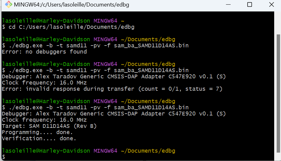
Now we can abandon the programmer and move on to board programming via USB.
Arduino setup
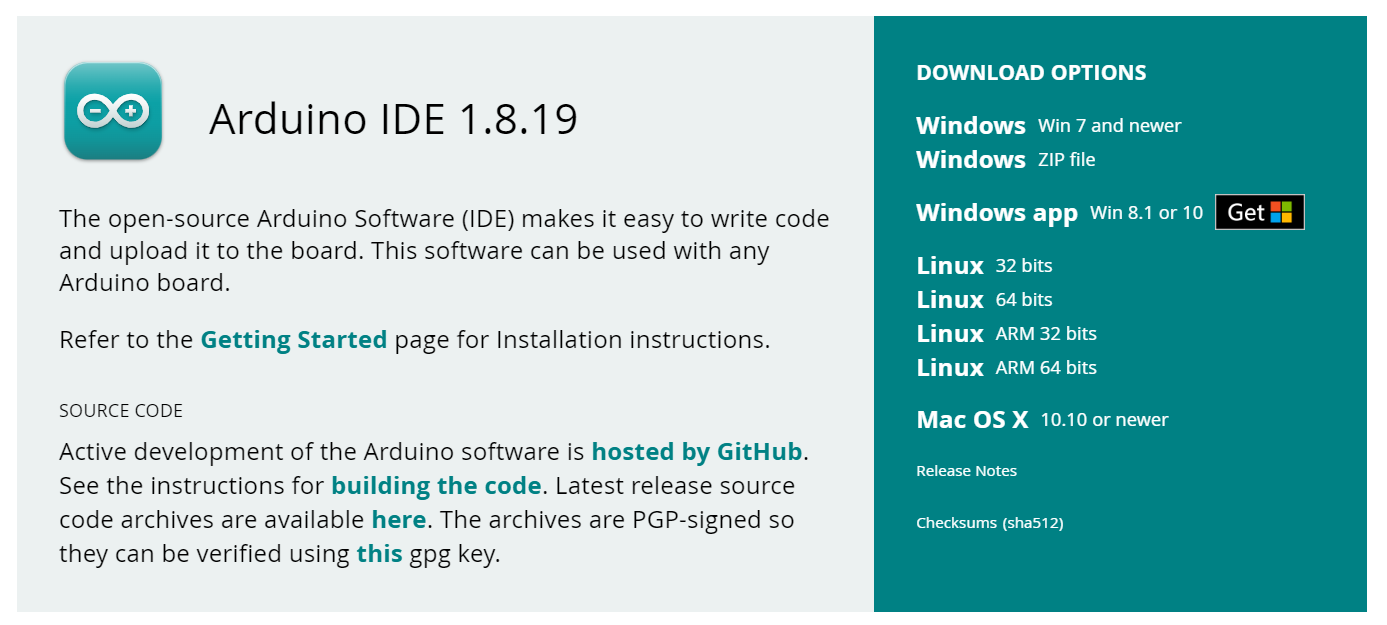
In order to be able to program the board, I used the Arduino software, but I needed an old version of the program, so I went to the software site again.
To set up the program I started following the step by step instructions in this document.
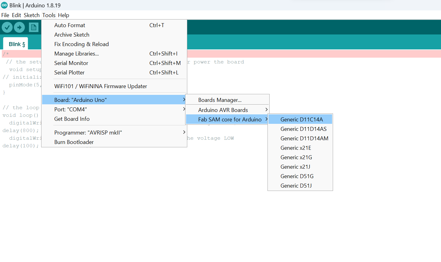
- file -> preferences -> additional board manager URLS
add this link: *https://raw.githubusercontent.com/qbolsee/ArduinoCore-fab-sam/master/json/package_Fab_SAM_index.json*
now arduino will be able to find the “board definitions” when we do:
- tools -> board -> board manager
search for Fab SAM core for Arduino
hit install
After that I chose my microcontroller from the list
Programming
On my board I have 3 LED lights - one for power, two to program. And I wanted to start playing with them. I decided to start simple - make the light blink. To do this, I used the code that I came up with in the Embedded Programming week, changing the timing a bit.
// the setup function runs once when you press reset or power the board
  void setup() {
// initialize digital pin 13 as an output.
  pinMode(13,OUTPUT);
}

// the loop function runs over and over again forever
void loop() {
  digitalWrite(6,HIGH); // turn the LED on (HIGH is the voltage level)
delay(800);              // wait for 0.8 second
  digitalWrite(6,LOW);  // turn the LED off by making the voltage LOW
delay(800);              // wait for 0.8 second
}
How did I know which number corresponds to the light pin on my microcontroller? I used the pin map I found here.
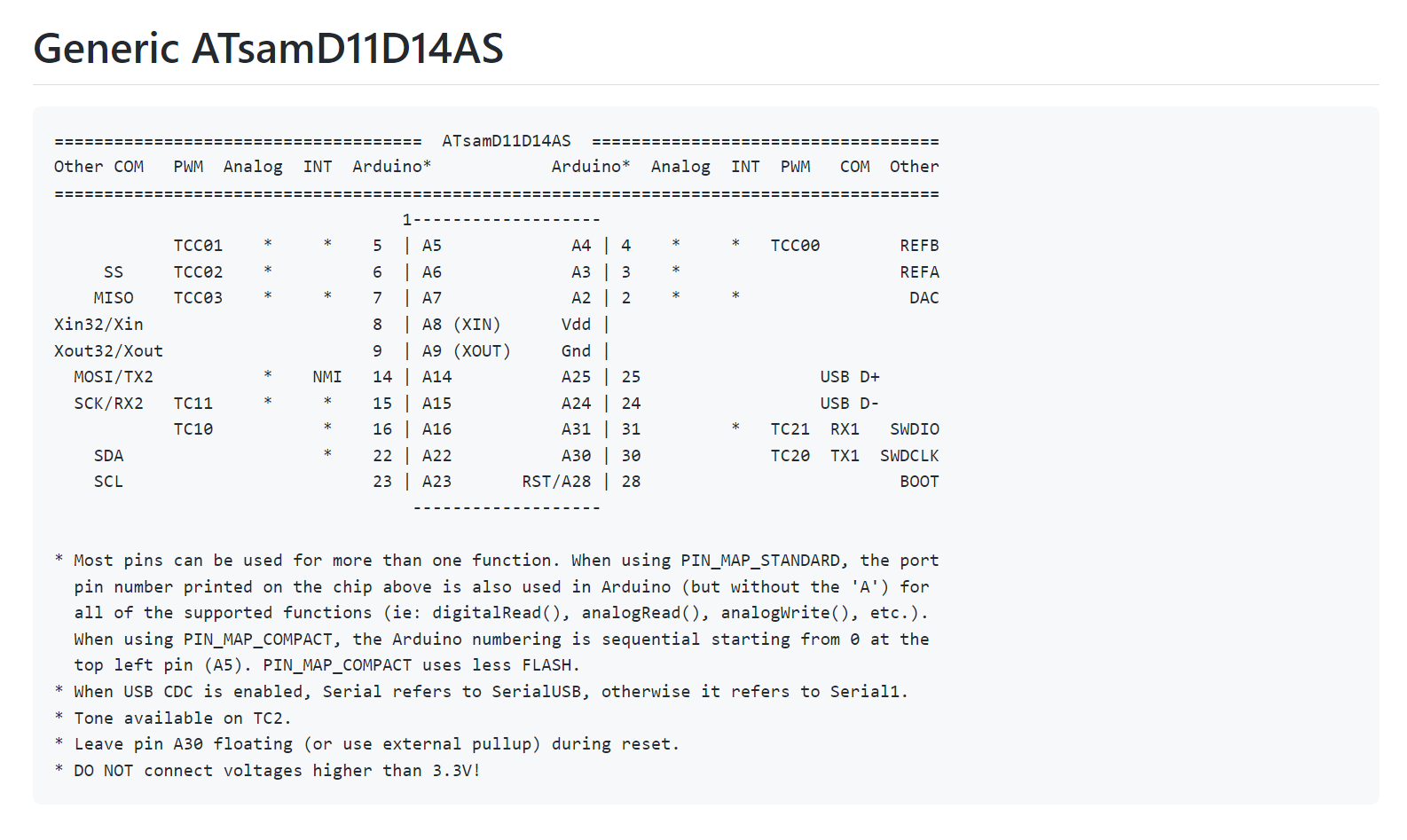
In this case, the 2 LEDs that I can program correspond to the numbers 5 and 6 in the Arduino.
Looking at this little light was happiness!!
But what is the use of two LEDs if only one of them is flashing?! I needed a code that made 2 lights blink.
So I asked my “friend” Chat GPT for little help:
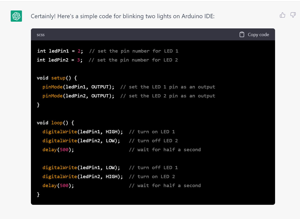
Here I have the universal code and I need to replace 2 and 3 by 5 and 6.
int ledPin1 = 5;  // set the pin number for LED 1
int ledPin2 = 6;  // set the pin number for LED 2

void setup() {
  pinMode(ledPin1, OUTPUT);  // set the LED 1 pin as an output
  pinMode(ledPin2, OUTPUT);  // set the LED 2 pin as an output
}

void loop() {
  digitalWrite(ledPin1, HIGH);  // turn on LED 1
  digitalWrite(ledPin2, LOW);   // turn off LED 2
  delay(500);                   // wait for half a second

  digitalWrite(ledPin1, LOW);   // turn off LED 1
  digitalWrite(ledPin2, HIGH);  // turn on LED 2
  delay(500);                   // wait for half a second
}
I also played with timing and the night show is ready! :)