Electronics Design
Task: Electronics Design
Group assignment:
- Use the test equipment in your lab to observe the operation of a microcontroller circuit board (as a minimum, you should demonstrate the use of a multimeter and oscilloscope)
- Document your work on the group work page and reflect what you learned on your individual page
Individual assignment:
- Design a development board to interact and communicate with an embedded microcontroller
Group Assignment
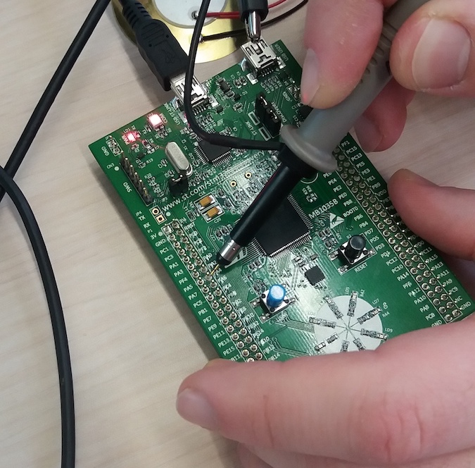
During our workshop with our second instructor, Onik Babajanyan, we had the opportunity to learn about and work with an oscilloscope.
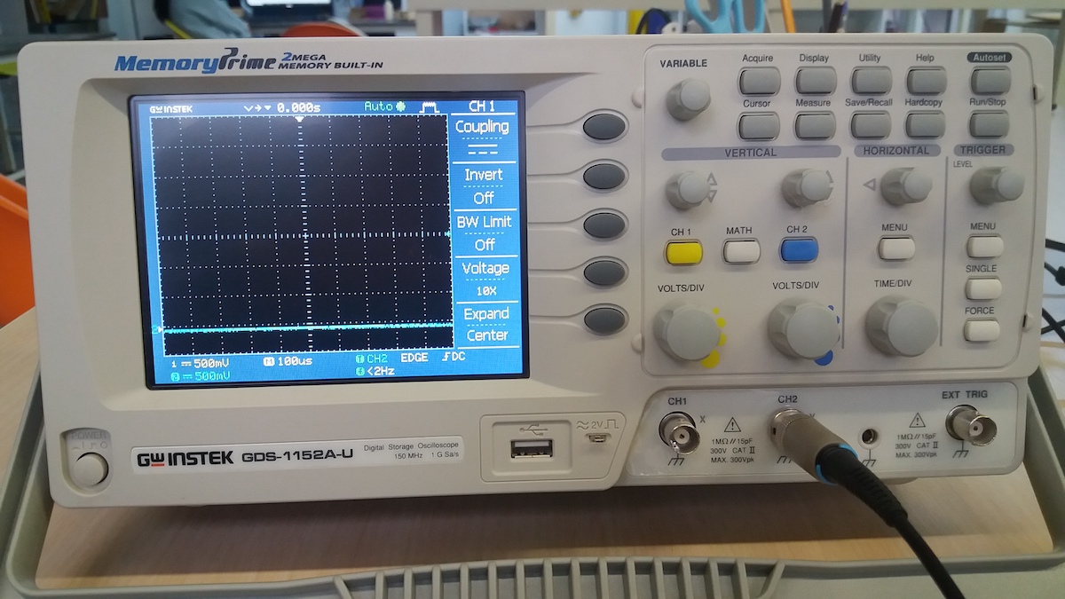
To demonstrate the oscilloscope’s capabilities, Onik aimed to generate a sine function and a periodic ramp function. While generating these signals directly with the Arduino board would be challenging due to the lack of a digital-to-analog converter, we discovered that the STM32 microcontrollers available in the Fablab have a built-in DAC (Digital-to-Analog Converter).
To generate the code for the sine and ramp functions, we turned to chatGPT for assistance. By leveraging its capabilities, we obtained the necessary code snippets to generate the desired signals.
The workshop provided us with valuable hands-on experience, enhancing our knowledge of signal visualization and the effective utilization of microcontrollers and oscilloscopes in various projects.
You can discover more about our Group Assignment here
Useful links
To familiarize myself with KiCad, I began searching for information and helpful videos on YouTube. During my search, I came across two video tutorials that provided me with a general understanding of how this software operates.
Installing Kicad and libraries
This week has been a momentous discovery in my life. I never imagined that electronics would become a part of my journey. However, from the very first day I stepped into the fab lab, the realm of electronics has intrigued and captivated me. This week, I had the opportunity to delve into the mysterious and fascinating world of circuit design through the software KiCad. It has opened up a whole new realm of possibilities, allowing me to create circuit boards and explore the intricacies of electronic design.
I downloaded the KiCad software here.

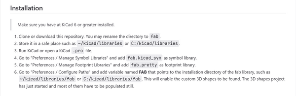
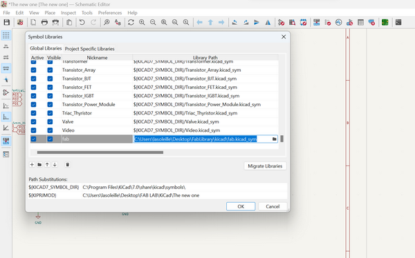
To install the Fab Library for KiCad, I followed those steps:
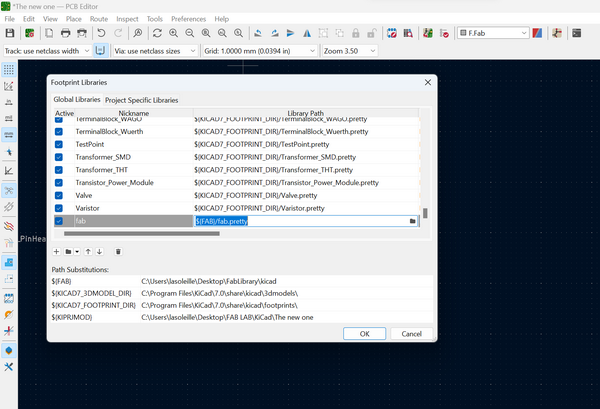
PCB Schematic
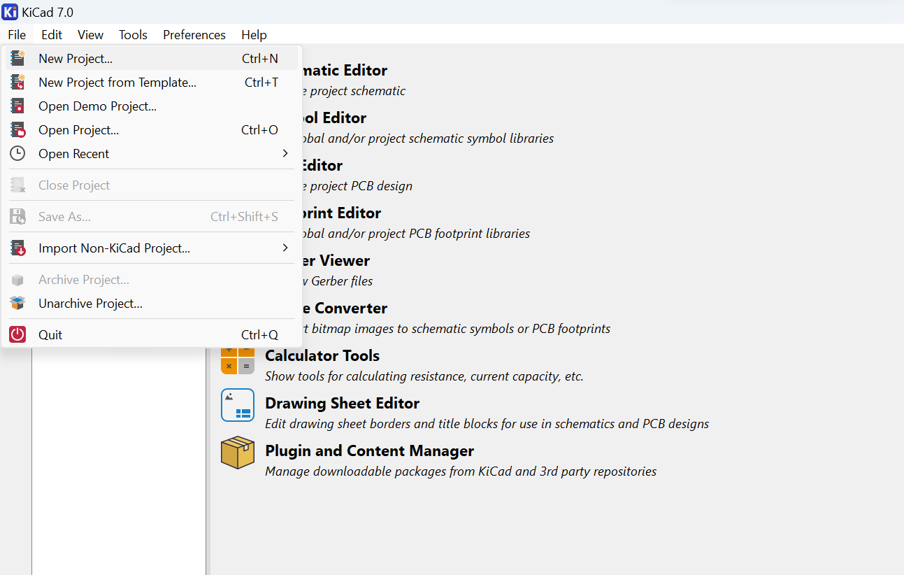
To create a new project in KiCad I selected File -> New Project.
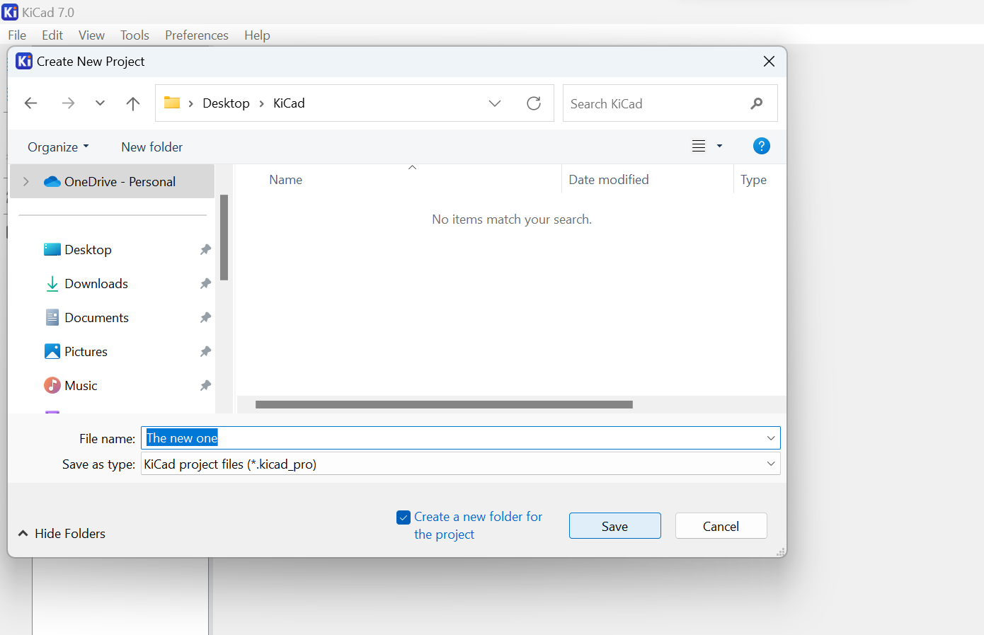
Here I named my project: it’s my first project ever and I called it The new one.
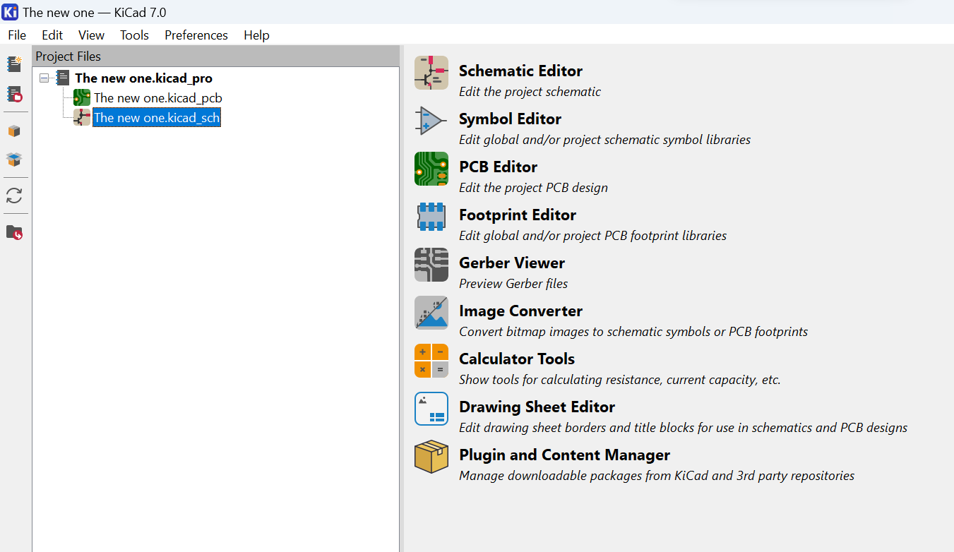
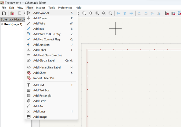
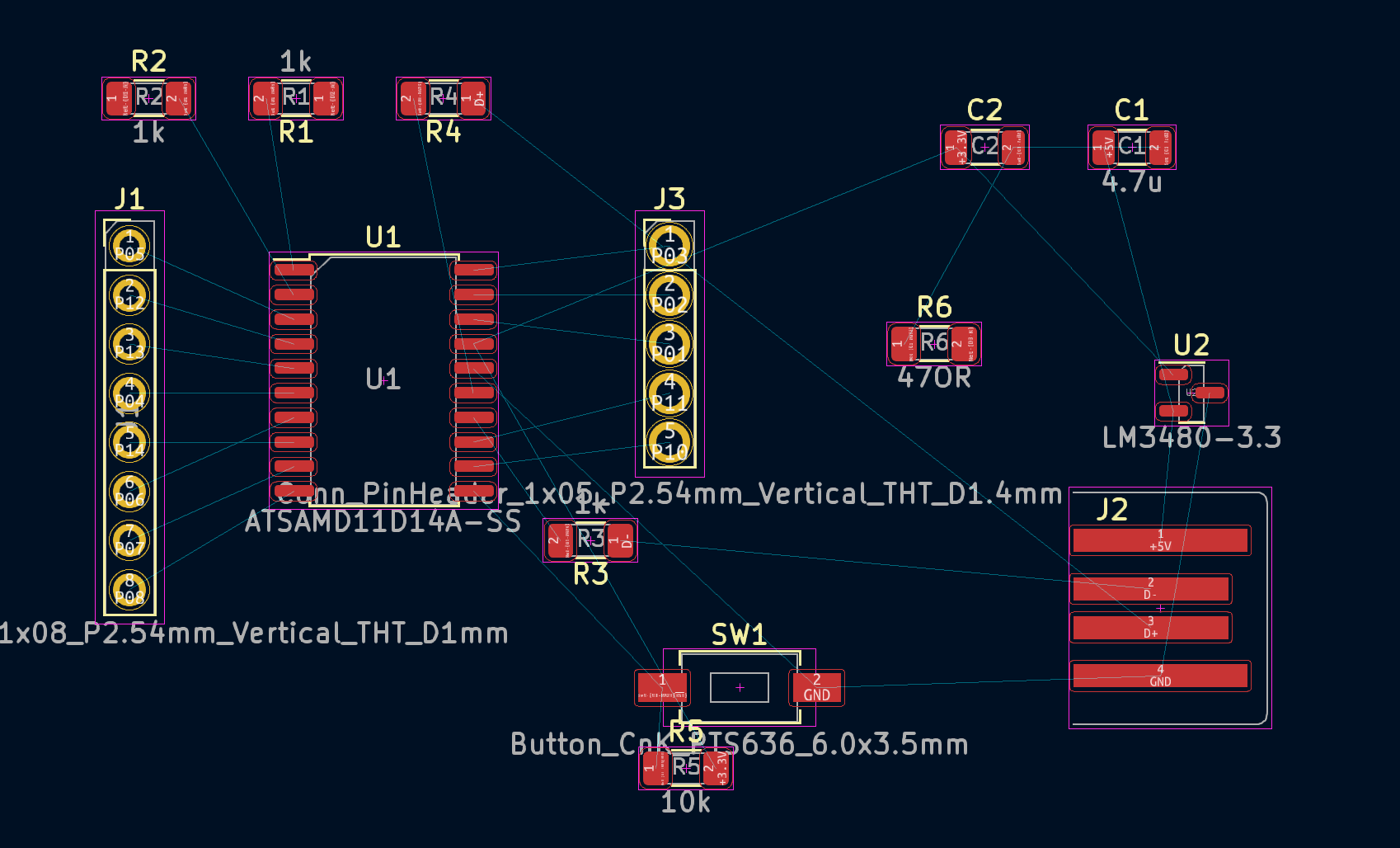
Now it’s time to make the schematic for my board. I selected the Schematic Editor:
First, I needed to grasp the logic behind creating a schematic for a circuit board.
During the initial stages of my project, I received valuable advice from Onik, who guided me on the essential components to include on my board. Here are the recommendations he provided:
-
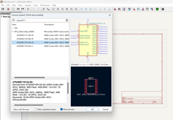
Microcontroller (ATSAMD11): Onik suggested incorporating a microcontroller to serve as the brain of the installation.
-
USB Power Supply: This allows for easy connection to a power source and ensures a stable power input for the microcontroller and other electronic components.
-
LED: The LED can serve as a visual indicator, providing feedback on the status of the installation or signaling specific events or interactions.
-
Voltage Regulator: To regulate the voltage levels and ensure a consistent and safe power supply, is recommended adding a voltage regulator to the board. This component helps maintain a steady 5V output, which is crucial for powering the microcontroller and other sensitive electronic components.
-
Reset Button: The button allows for easy resetting of the microcontroller or any connected circuits, providing a simple way to troubleshoot or initiate specific actions.
-
Connectors for Pins: To facilitate the connection and interaction with external devices or components. These connectors enable easy integration of additional sensors, motors and other devices.
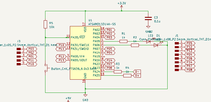
I started with the microcontroller:
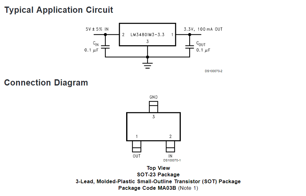
The next step was the voltage regulator. I used the LM3480 regulator. In the datasheet I found information about the schematic and connection:
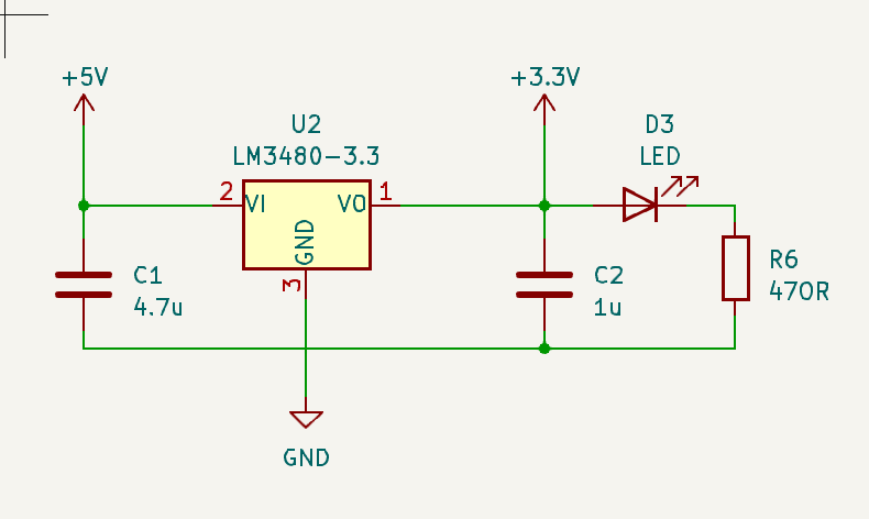
I noticed that our instructor, Onik Babajanyan, used different capacitors in his schematic.
In this case, I wanted to clarify the specific function of the capacitor and its role within the circuit board.
In this source I found interesting information about the capacitors. Some important points:
-
Stability and Filtering: Capacitors help stabilize the output voltage of the regulator by reducing voltage fluctuations and ripple caused by variations in the input voltage or load conditions. They act as a buffer, providing additional energy when needed and absorbing excess energy when the demand decreases.
-
Noise Reduction: Capacitors can effectively filter out high-frequency noise present in the input or output voltage. They act as a low-pass filter, attenuating unwanted noise and providing a cleaner and more stable output voltage.
-
Transient Response: Capacitors enable the voltage regulator to respond quickly to sudden changes in the load. They can supply additional current during transient events, ensuring that the output voltage remains within the desired range and minimizing voltage droop or overshoot.
In this case, I decided to take precautions and use the capacitor from my instructor’s scheme to ensure its compatibility. Additionally, I added an LED to provide a visual indication of whether my board is functioning properly after soldering.
The next part of schematic is USB:
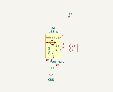
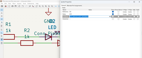
I also connected two LEDs to my microcontroller. However, upon checking, I realized that I had made an error at this stage. I had not properly connected the pins of the microcontroller to the external pins.
I added connentors for pins:
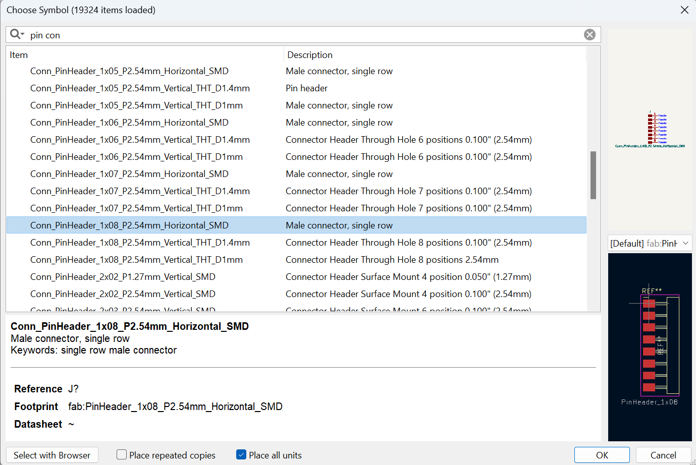
Now it’s time to associate footprints with each component in the schematic. Footprints define the physical layout and dimensions of the components on the PCB. KiCad provides a library of pre-defined footprints, but you can also create custom footprints if needed.
To associate footprints with each component in KiCad, you can follow these steps:
-
Right click on the component for which you want to associate a footprint. The component properties should appear in the right-hand panel.
-
In the component properties panel, locate the “Footprint” field. Click on the dropdown arrow to see the available footprints. KiCad provides a library of pre-defined footprints that you can choose from.
-
Select the appropriate footprint for your component from the dropdown list. The footprints are categorized based on the component type and package. You can use the search function to find the desired footprint.
-
Double-check that the selected footprint matches the physical package of your component.
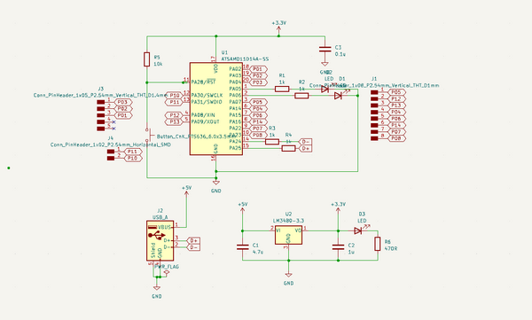
Here is the PCB schematic after few changes:
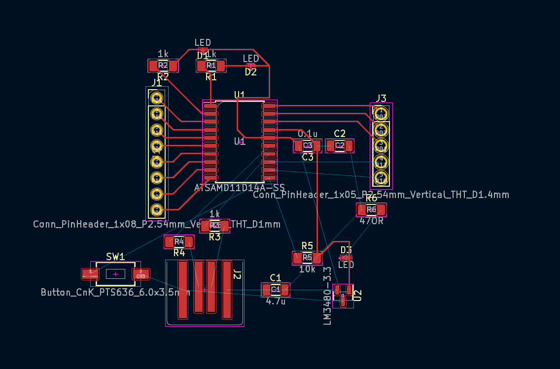
PCB Design
When all the connections on the schematic have been verified and all the components’ footprints are correctly placed, you can proceed with confidence to designing the board.
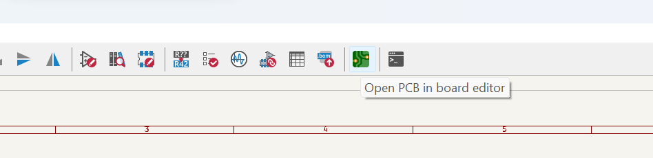
To accomplish this, at the top of the toolbar, you will find the tool to Open PCB in board editor.
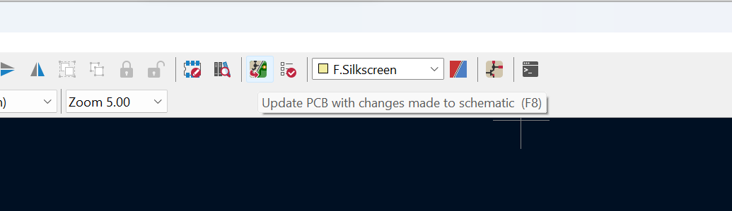
Here, another tool becomes useful for applying all the changes made in the schematic.
This painting calls From chaos to order!
At this stage, I felt overwhelmed and doubted if I could successfully connect all these components into a functional board. However, by taking it step by step, I started noticing progress. Using helpful tools like flipping the components using the R key on the keyboard, I gradually moved closer to achieving the desired result.
When working on PCB design in KiCad, there are several lifehacks or useful techniques that can help streamline the process and enhance your efficiency. Here are a few that I used:
-
Shortcut keys: KiCad offers numerous shortcut keys that can greatly speed up your workflow. Familiarize yourself with commonly used shortcuts for tasks like zooming in and out, rotating components, and placing tracks.
-
Grid and Snap settings: Adjusting the grid and snap settings in KiCad can make it easier to align and position components precisely. Use smaller grid sizes for fine details and larger grid sizes for general placement.
-
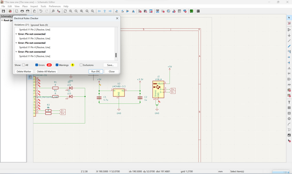
DRC (Design Rule Check): Utilize the DRC feature to automatically check your design for common errors such as clearance violations, overlapping tracks, or unconnected pins. Running the DRC regularly helps catch potential issues before fabrication.
-
Copper pour: Utilize copper pour areas to create large ground planes or power planes.
Filling with GND, also known as copper pour or ground plane, is a technique used in PCB design to create a continuous copper area connected to the ground (GND) signal. It helped me a lot to avoid manually connecting all the GNDs together with individual traces.

To create a copper pour in KiCad, you can use the “Zone” tool.
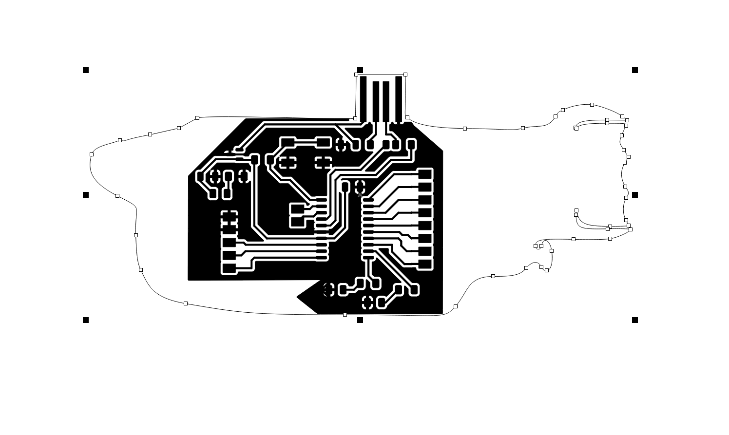
Here what I got!
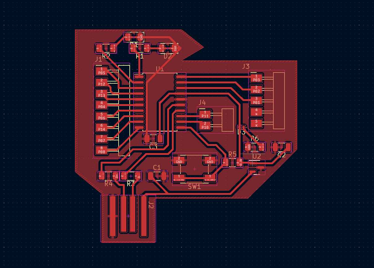
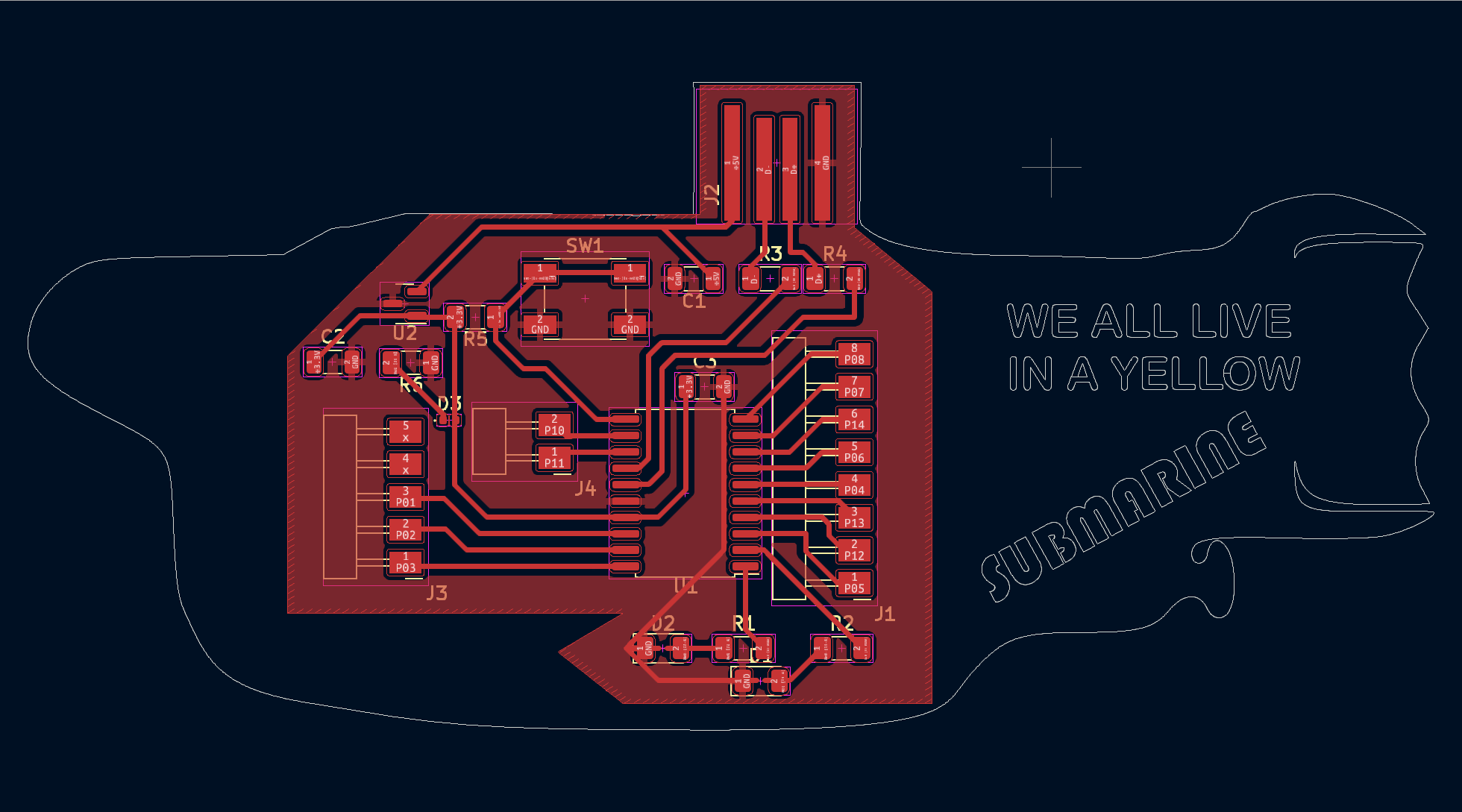
A shape for a board

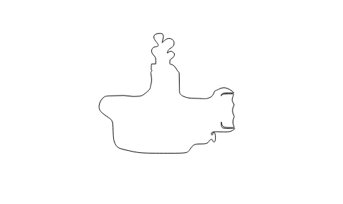
The next step was to find a shape (cutout) for my board. During the creation process, I had the image of the Beatles’ “Yellow Submarine” in my mind. Therefore, I searched for a .png file of the submarine, converted it to .svg format, and began working on it in CorelDraw. To ensure the precise size of my board, I exported the traces file as an .svg and imported it into CorelDraw as well.
I made adjustments and modifications to match the shapes, and I also added lyrics from the song.
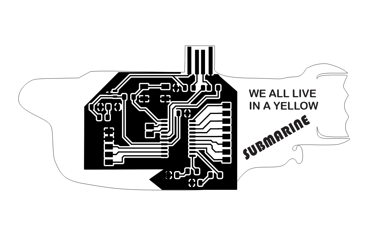
To ensure that the text would be treated as a single line for cutting purposes, I converted the text to curves.
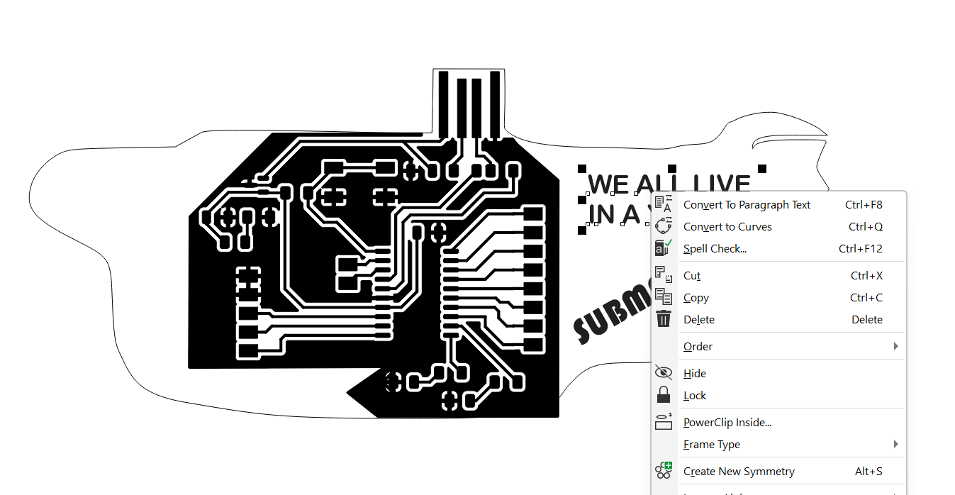
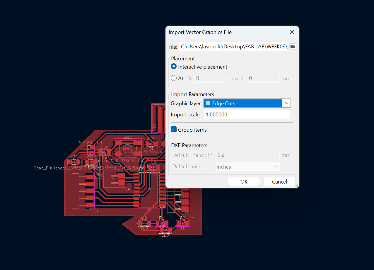
Once I finished editing my drawing, I exported it as an .svg file and imported it into KiCad.
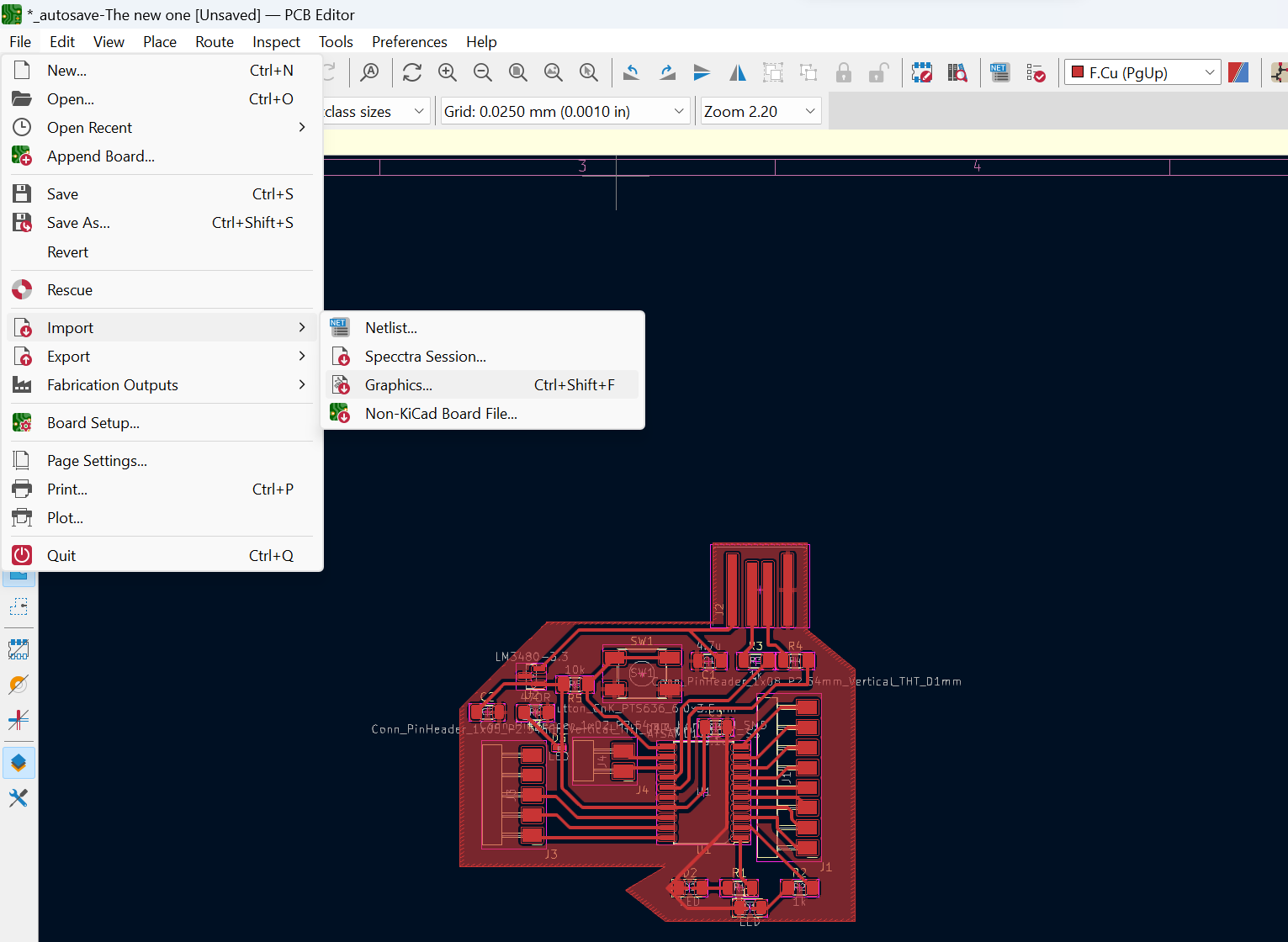
We need to select the Edge Cut layer to import our drawing as a graphic file. Only in this case will the software recognize it as the drawing intended for cutting.
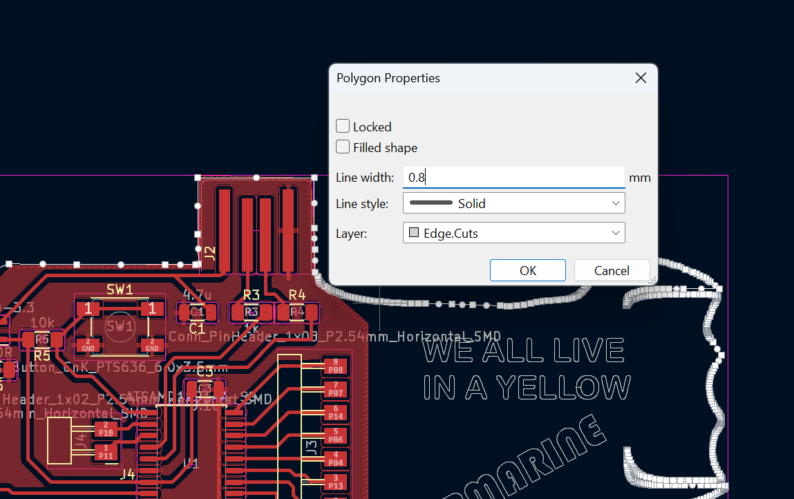
Since the mill I intend to use for cutting is 1/32 inches (approximately 0.8mm), I enlarged the width of the cutting line track to 0.8mm.
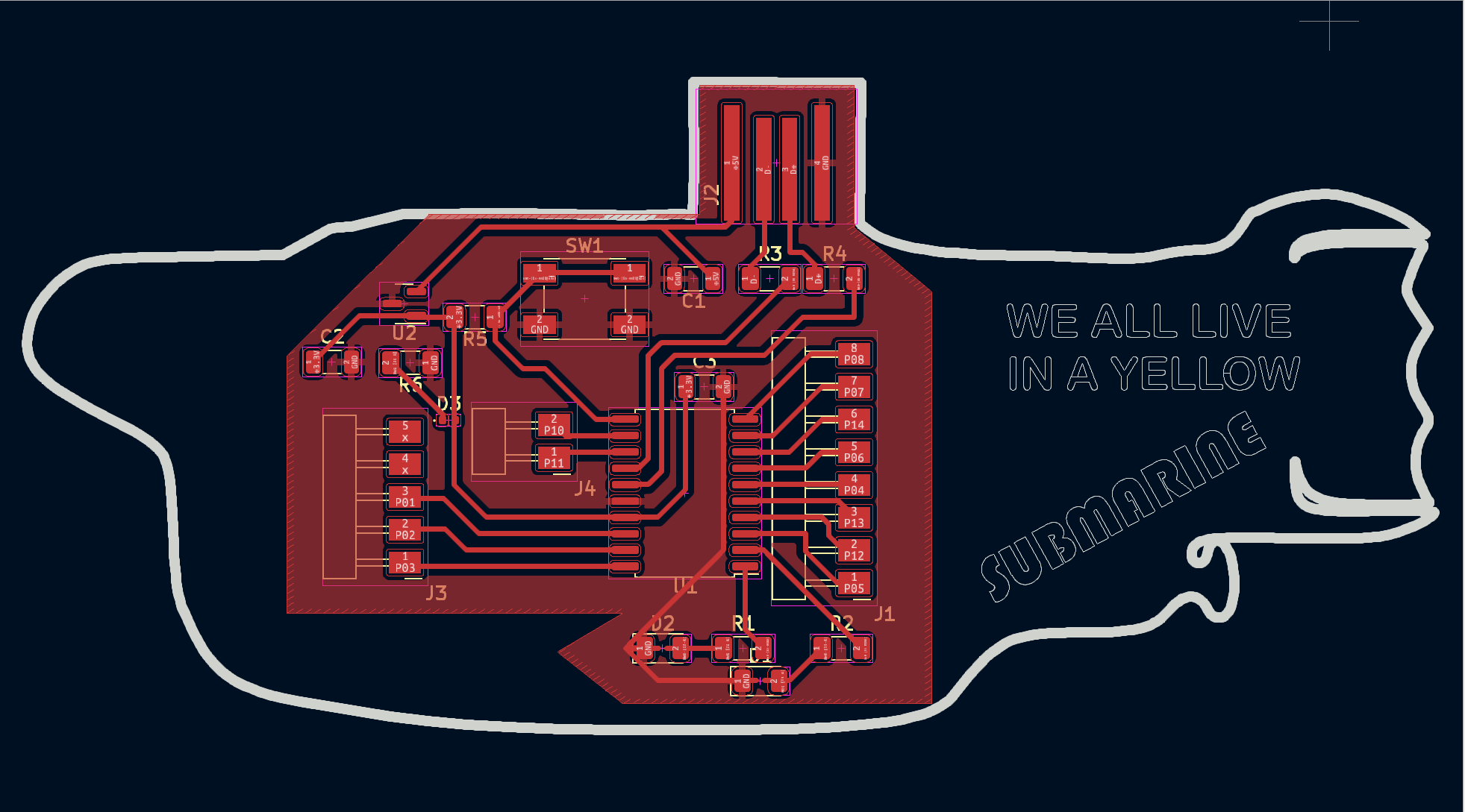
Here is my Submarine board ready to machining!
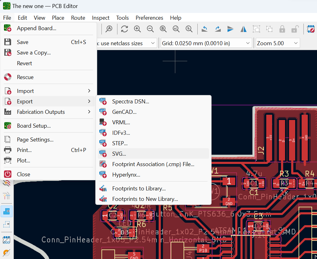
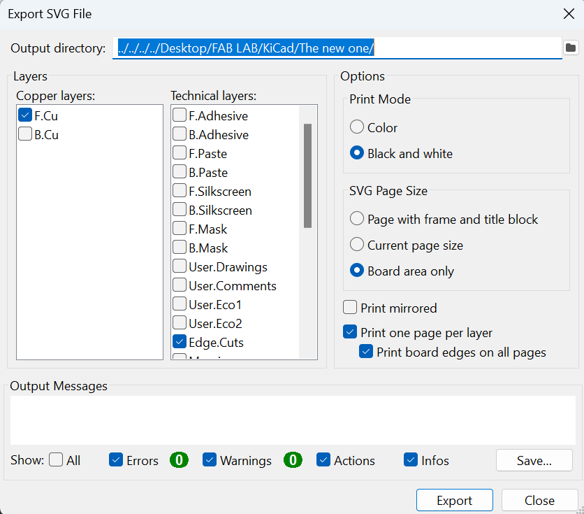
Export
Conclusion
Embarking on my first steps in electronics has been a transformative experience, opening up a whole new world of possibilities and knowledge.
One of the most significant aspects of these early steps is the exposure to the fundamentals of electronics. Through hands-on exploration, research, and guidance from experienced mentors, I have been introduced to key concepts such as circuitry, components, and their functionalities. This foundational knowledge forms the building blocks upon which I can further develop my skills and delve deeper into the intricacies of electronic systems.