4. Electronics production
This week was about electronics production. During the last year of high school, I was taking robotics classes. That was the first time I programmed a microcontroller. It was the time when I decided future of my education. At university, I started a part-time job for a company that makes automated solutions. I was working there as an embedded programmer. So, I have experience in embedded programming, but I have not produced my own PCB. This week I did it.
Our assignment for this week is
Group assignment.
characterize the design rules for your in-house PCB production process
extra credit: send a PCB out to a board-house
Individual assignment:.
make an in-circuit programmer that includes a microcontroller:
extra credit: customize the design
mill and stuff the PCB
test it to verify that it works
extra credit: try other PCB processes
GROUP ASSIGNMENT
Here is the link for our group assignment.
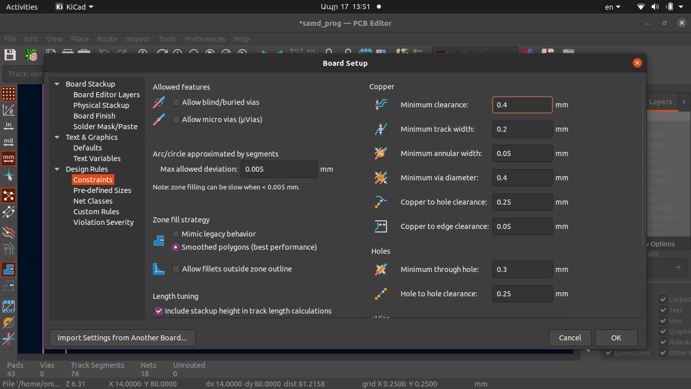
Below you can see the test cut. According to the results of my line test, 1/64 end mill is not able to cut lines less than 0.15mm.

After cutting two unsuccessful boards, I changed the design constraints in Kicad. If you set it up once, Kicad will ensure that there is no tiny track or connected tracks.
Make an in-circuit programmer
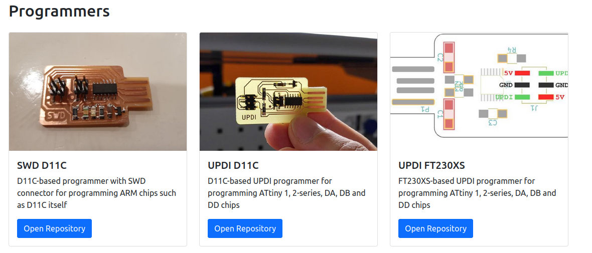
To make an in-circuit programmer, I searched at Fabacademy websites and found a board with the SAMD11C microcontroller, which I never used. You can find the summary for programmers of Fabacademy here.
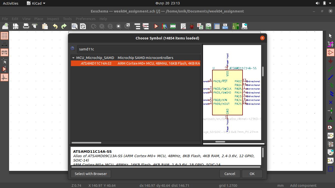
In the assignment is said that for extra credit, we need to customize the board. So, I decided to design a new one using Kicad. I used the Gitlab link of the SWD 11C project for a reference. After I found all the resources for the board, I read the SAMD11C’s datasheet.
So, to design a PCB, I need software for it. I downloaded Kicad as it is free and open-source.
To install Kicad, you need the command below
sudo apt install Kicad
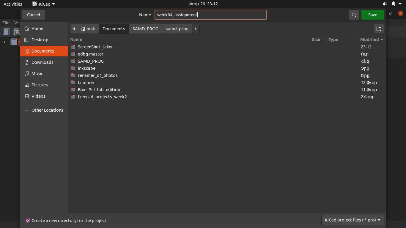
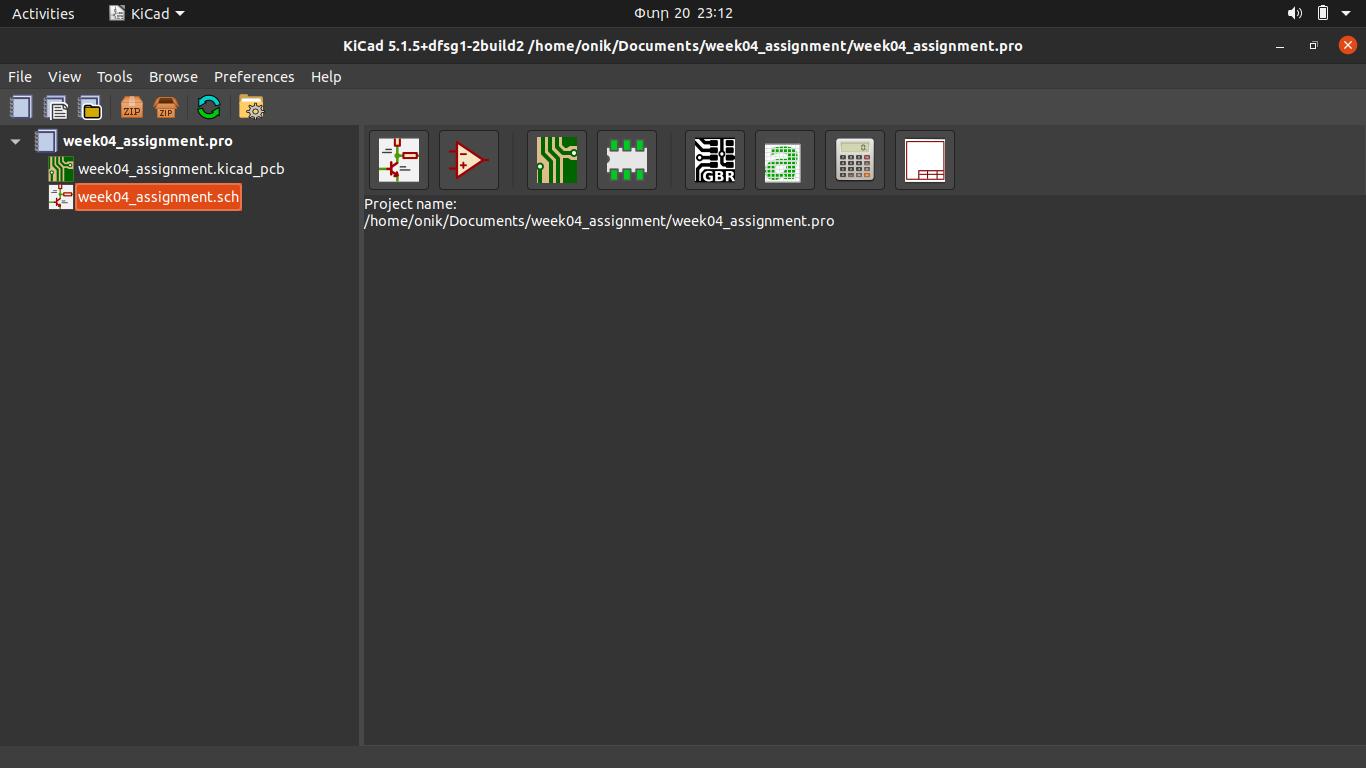
After having Kicad installed, I started a new project.


As you can see, Kicad creates two files. The first one is for layout design with a prefix of .kicad_pcb the second is for schematic design with a prefix .sch. At the start of a project, we need a .sch file to design a schematic capture of the board. At the schematic part, we need to put all the components and connections between them.
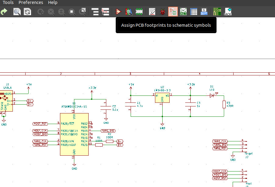
Schematic Design
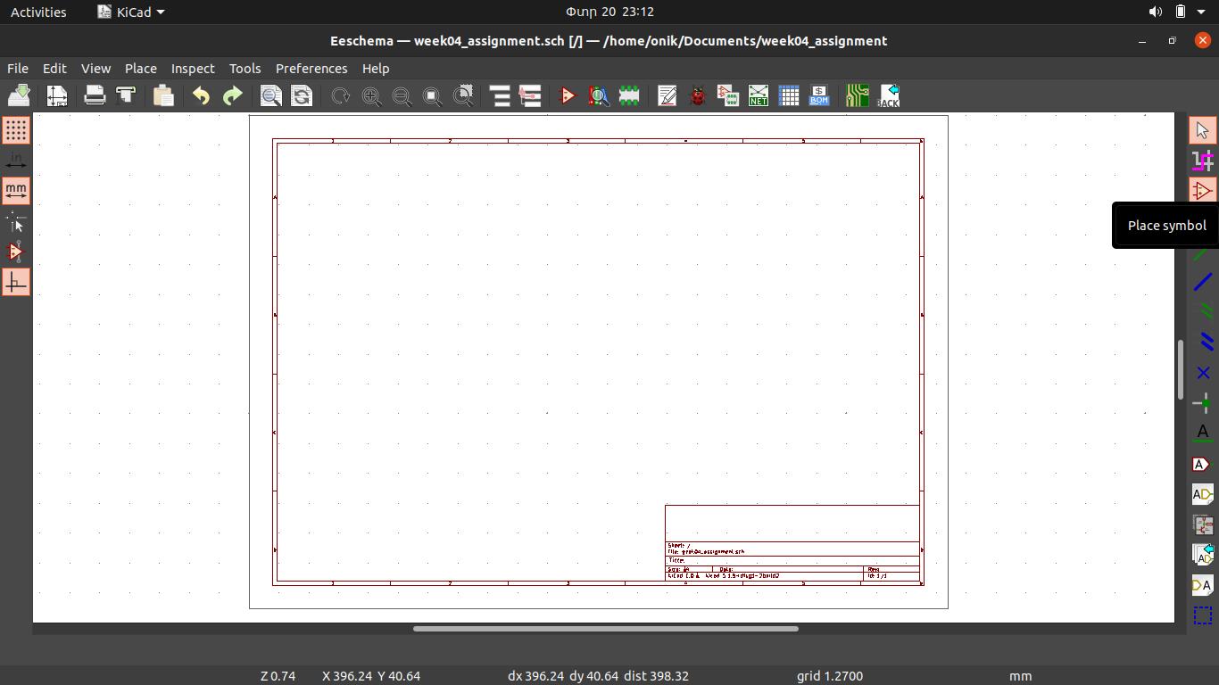
For placing symbols, we have a tool in a right part of the screen.
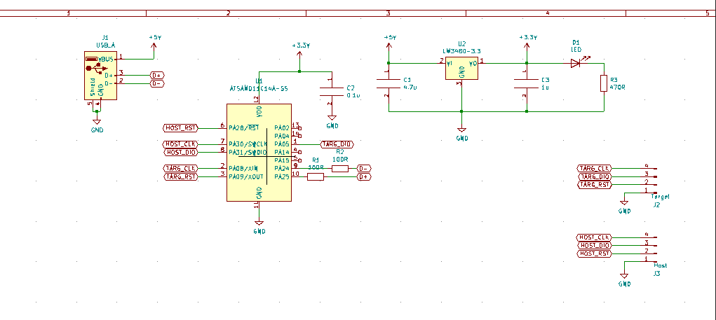
Kicad has a pretty decent parts library, so I found components without difficulty.

Here, I just typed the name of a microcontroller and found a schematic symbol for that.
Then, I searched for a 3.3V regulator that was lm3480.

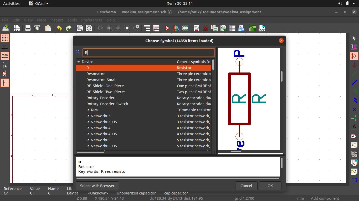
After, I added a few resistors for USB D- and D+ to limit the current and two capacitors for the input and output of a voltage regulator.

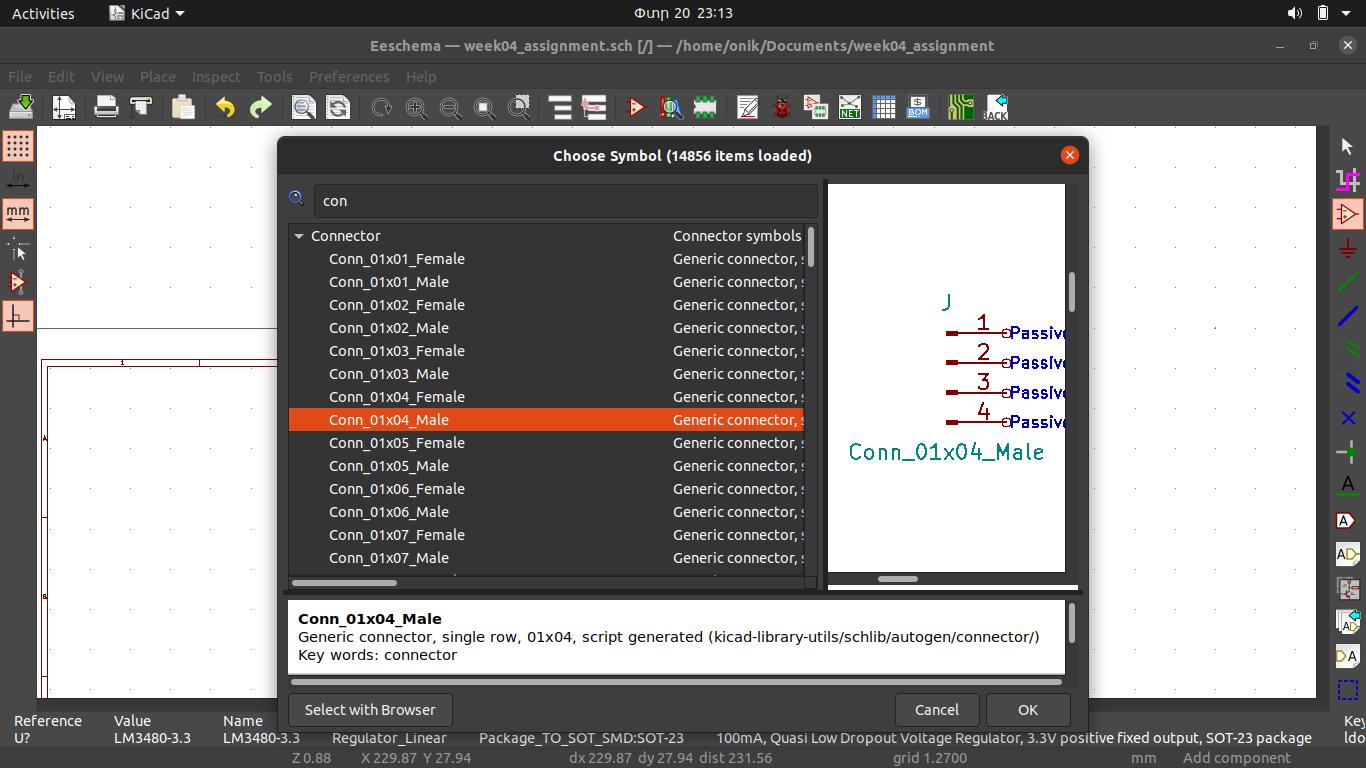
Adding two four-pin connectors, one for programming the board and one for programming the target board.
Having all components added, I added two power nets, one for 5V and one for 3.3V.
Kicad has a tool called the global label. To connect two pins, you need to connect them to a label with the same name. I used that labels to connect the pins of a microcontroller to the connectors. It makes the design clear and easy to read. This is the final schematic design. It is not so complicated and easy to read.
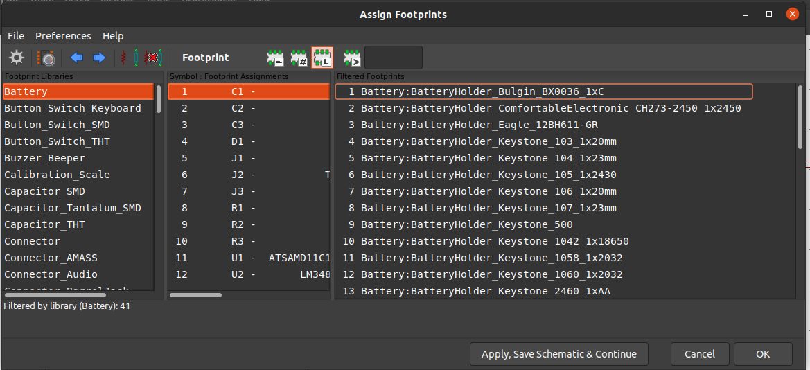
After having the schematic design done, you need to connect this file with the PCB design file. So, first, you need to assign footprints for the components you used. There is a tool for assigning footprints. It will automatically load all the footprints in a library. You need to choose one, or if there is not the needed one, you can design yours.
If all the components in the design have a footprint, you can start the PCB design.
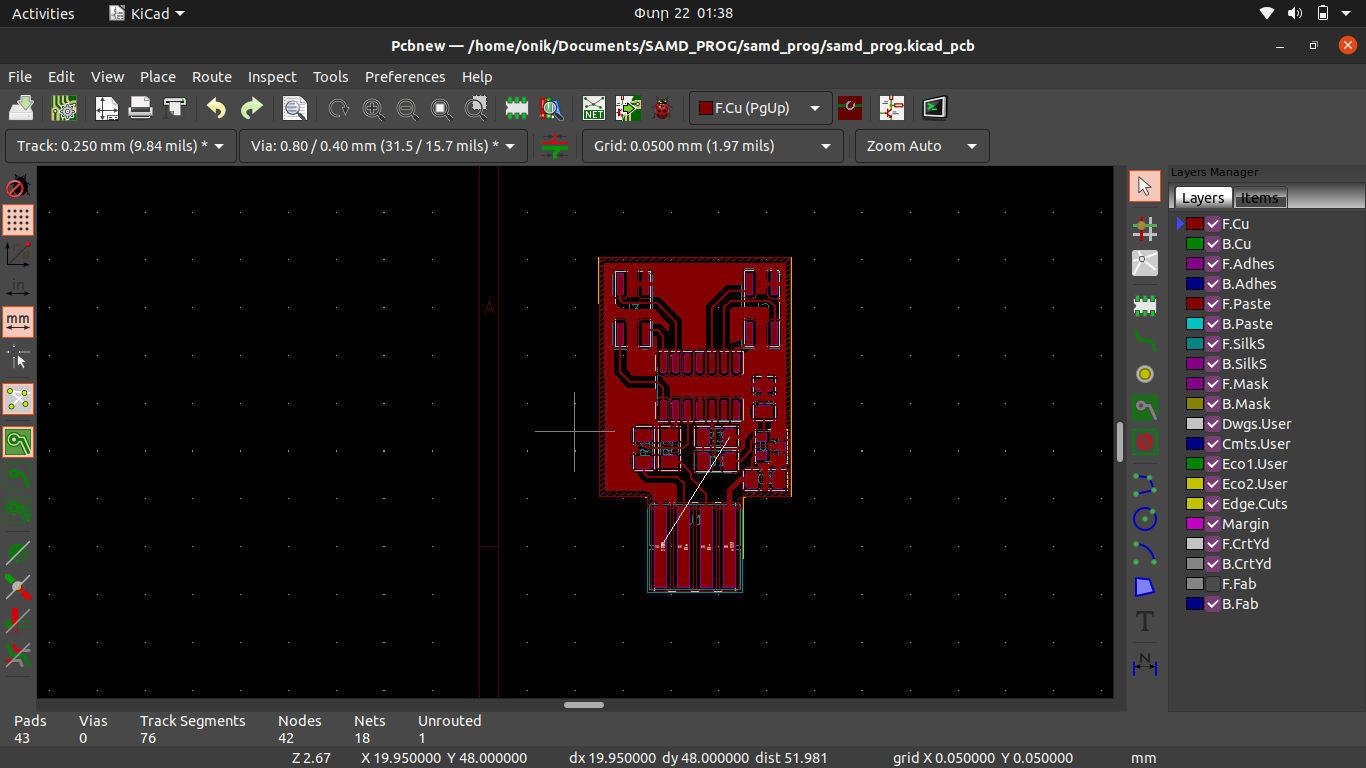
PCB Design
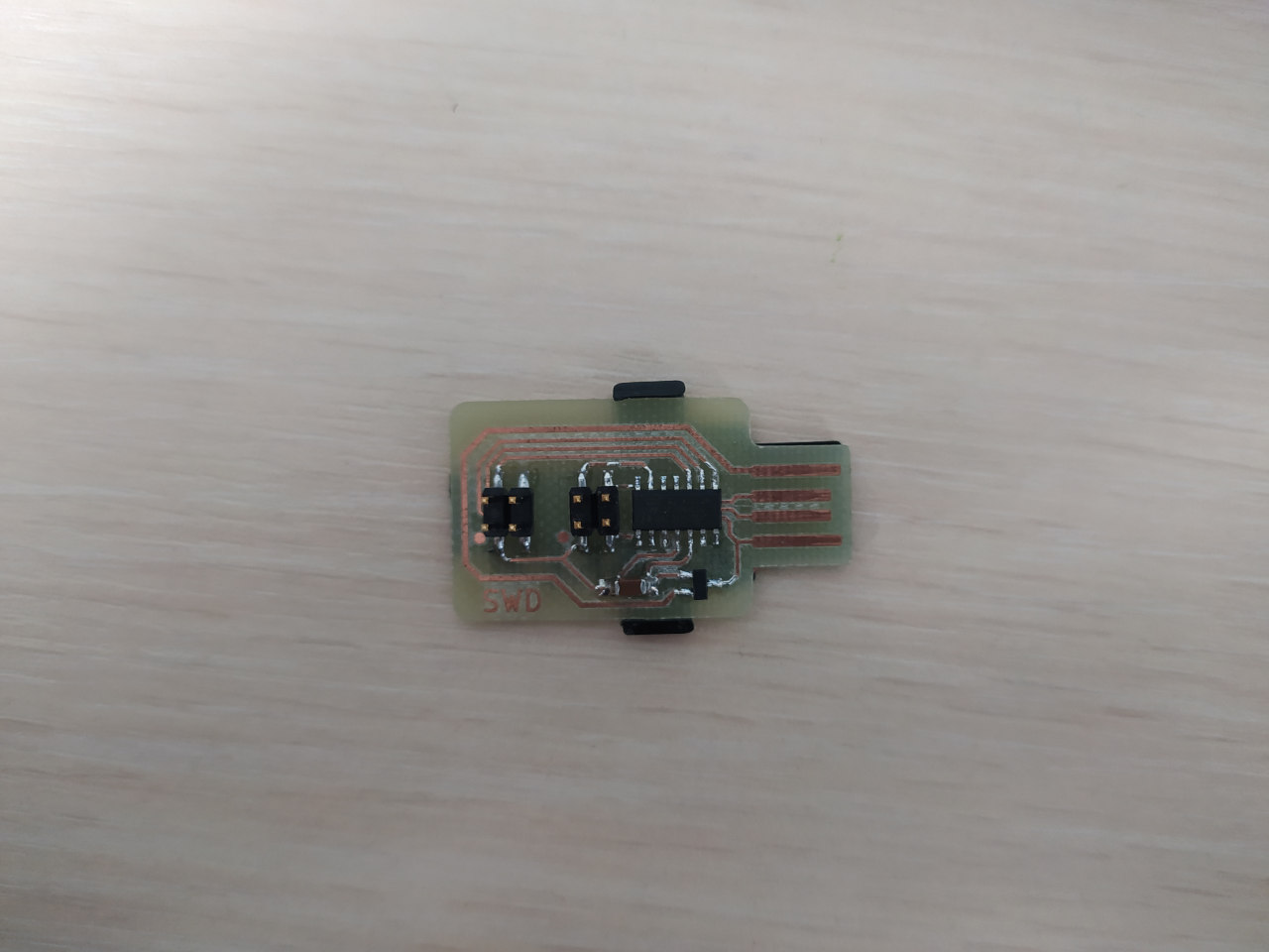
In this section, I was going to present how I did PCB design, but unfortunately, I missed all my screenshots. So, I will show you the result of the design, and after redesigning, I will add all the details.
Mill and Staff the PCB
So, having done the PCB design, I started the milling process. I checked different software like a Flatcam to export Gerber files for SRM-20, but I found Fab Mods the most straightforward and easy one. I checked different Fabacademy pages to be familiar with mods.
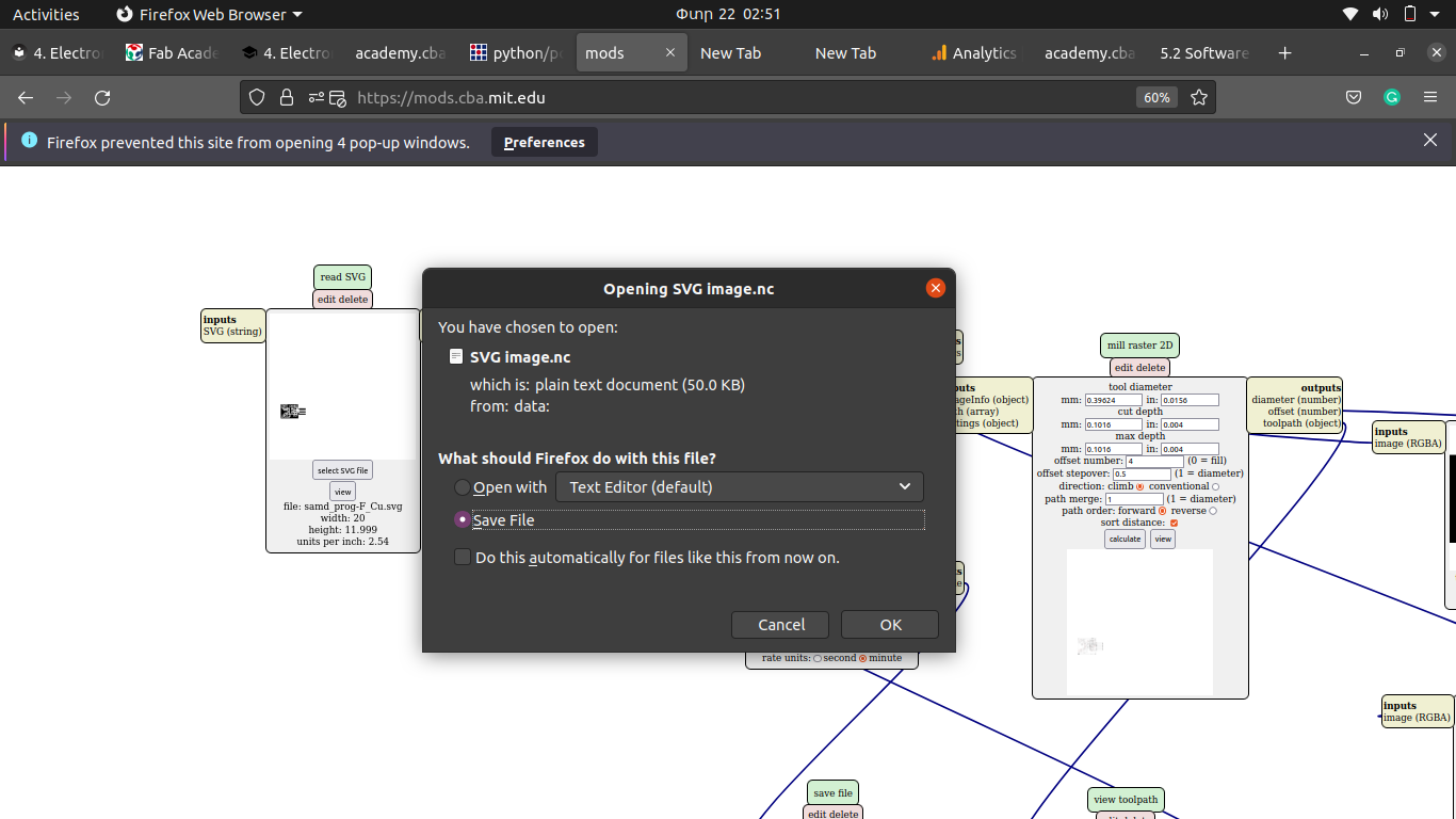
1.Open the Mods webpage and right-click to open the menu.
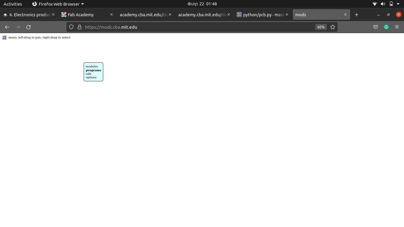
2.Click on programs.
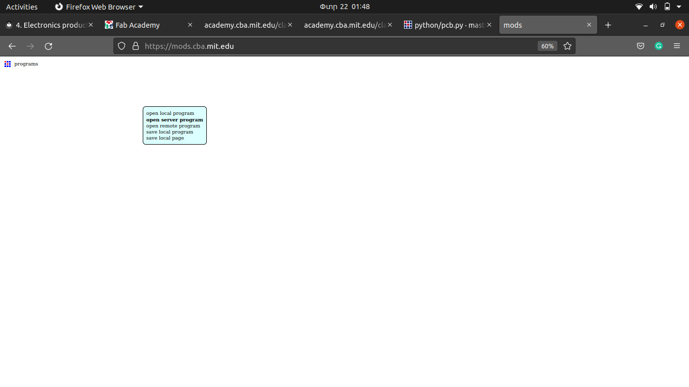
3.Choose an open server program.

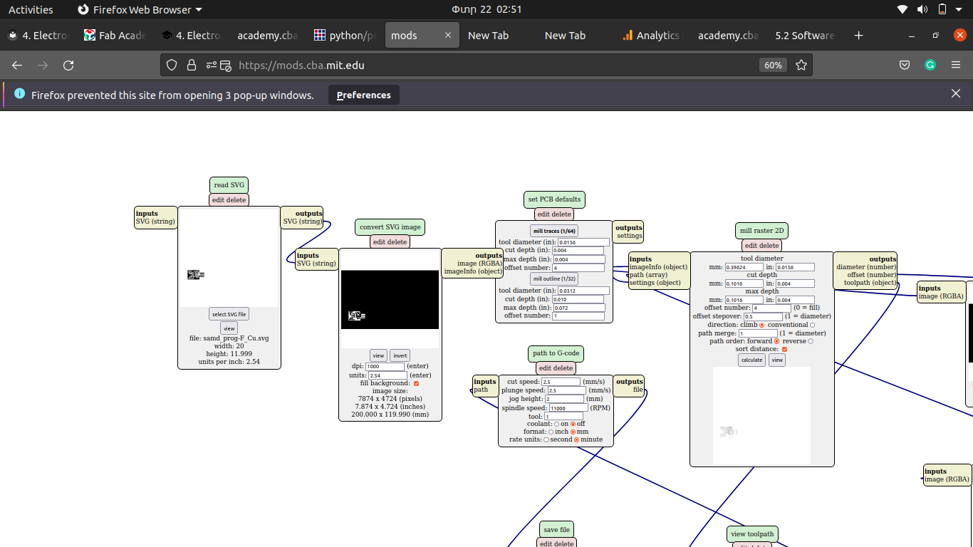
As you can see from image above you can choose different types of file. I used Kicad for my PCB design and I think the best one is SVG. Mods will show this window after selecting the desired option.
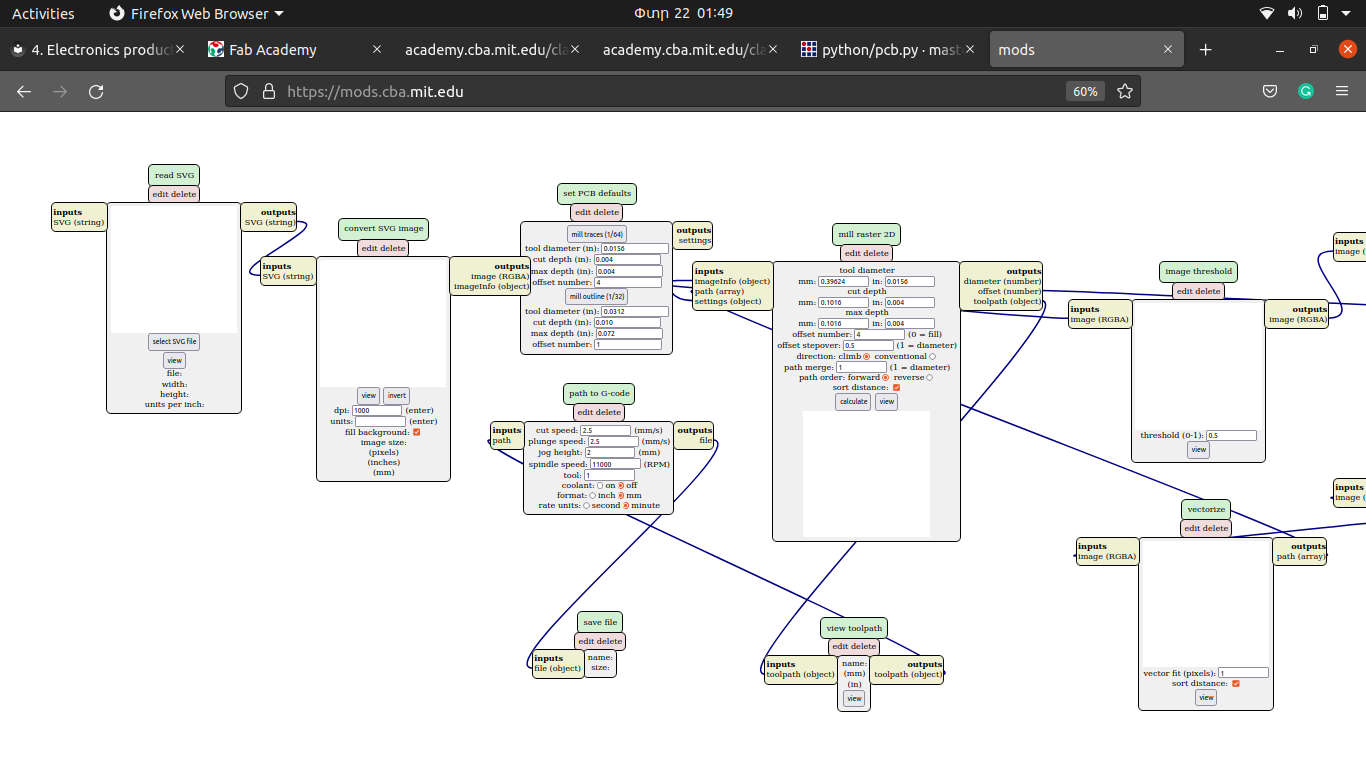
Please, notice that in the Mods, we have two options, one for milling traces and one for milling outline.

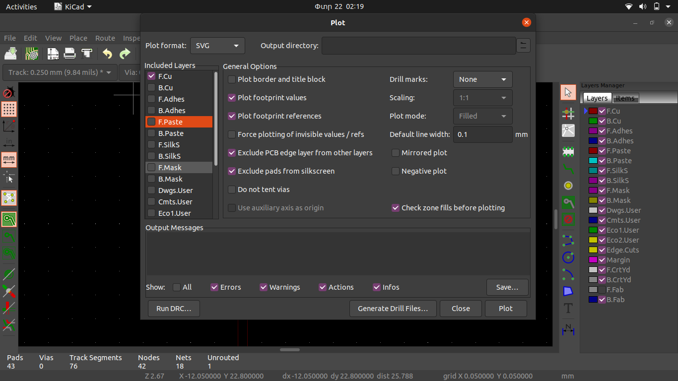
So, I need to export two files. In Kicad, to export files, you need to go to file -> plot. In this window, you choose a file format and the layers you want to export. Kicad will generate separate files for each layer. We need only two layers, the top one and the outline.

To start milling, we need a G-code format for SRM-20. So, I opened the top layer SVG file in mods, then inverted it as Mods understands black color as a cutting space. After I choose the mill traces(1/64th) option, then you need to click calculate button and the file for cutting will be downloaded.
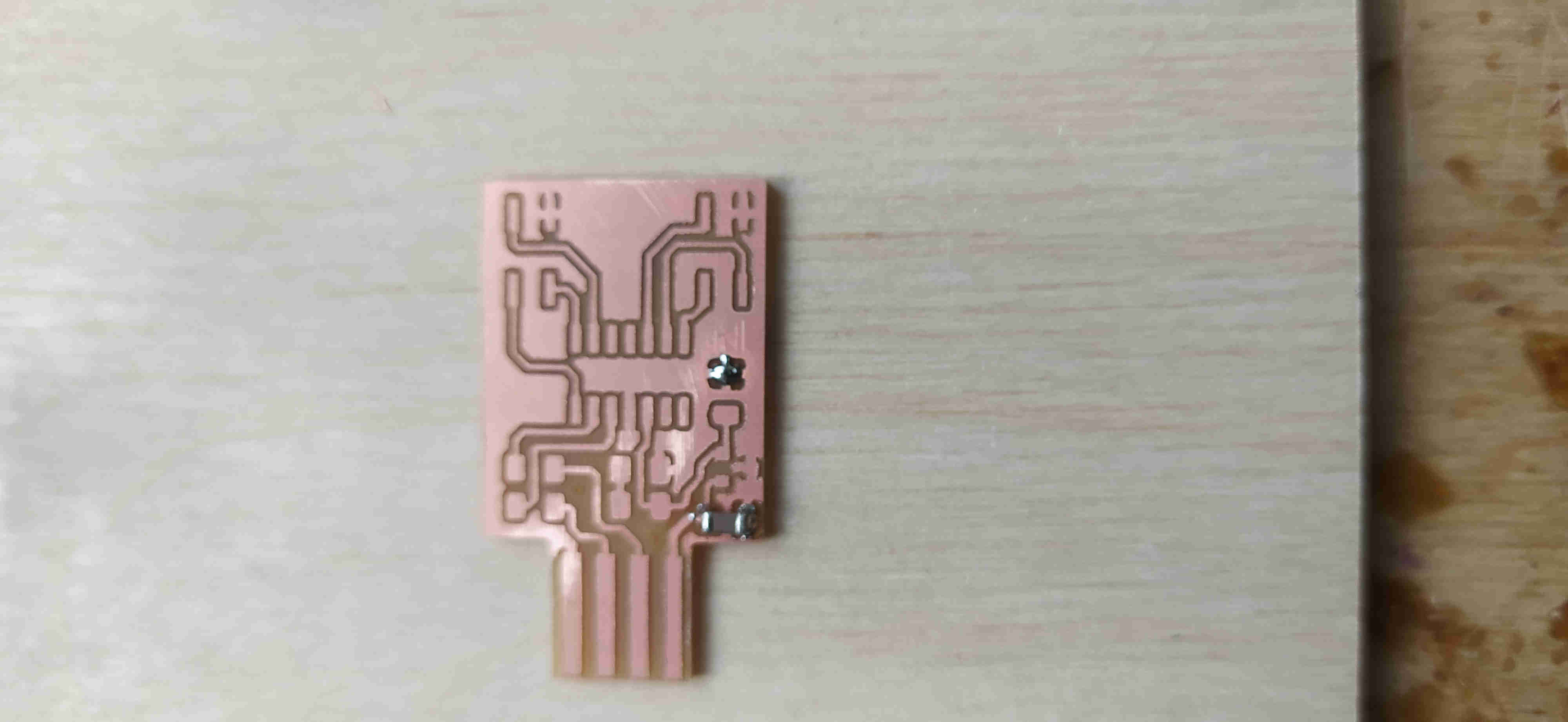
The .nc is a file format for G-code that SRM-20 needs to cut. Having G-code file ready, I put the material, set the origins of the machine and sent the job to the machine.
When the machine finished, I noticed that I had little derbies at the edges of traces. After I asked about the issue, Babken told me that the problem was the cutting direction. But I didn’t cut the board the second time. I just cleaned it with a tool(I don’t know the name of the tool in English).
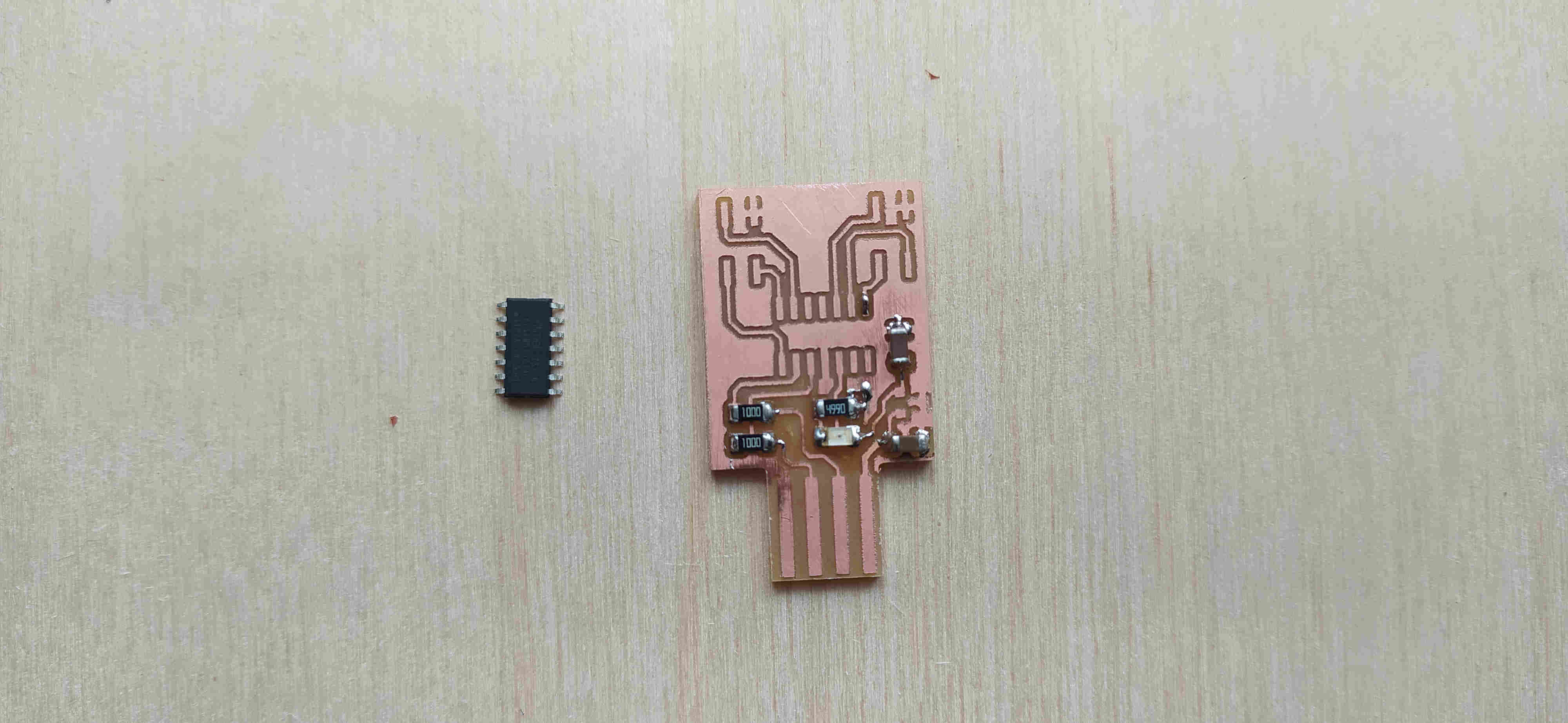
After having the working board, I used Adrian Torres’s Samdino tutorial to burn the programmer .bin file to the board.
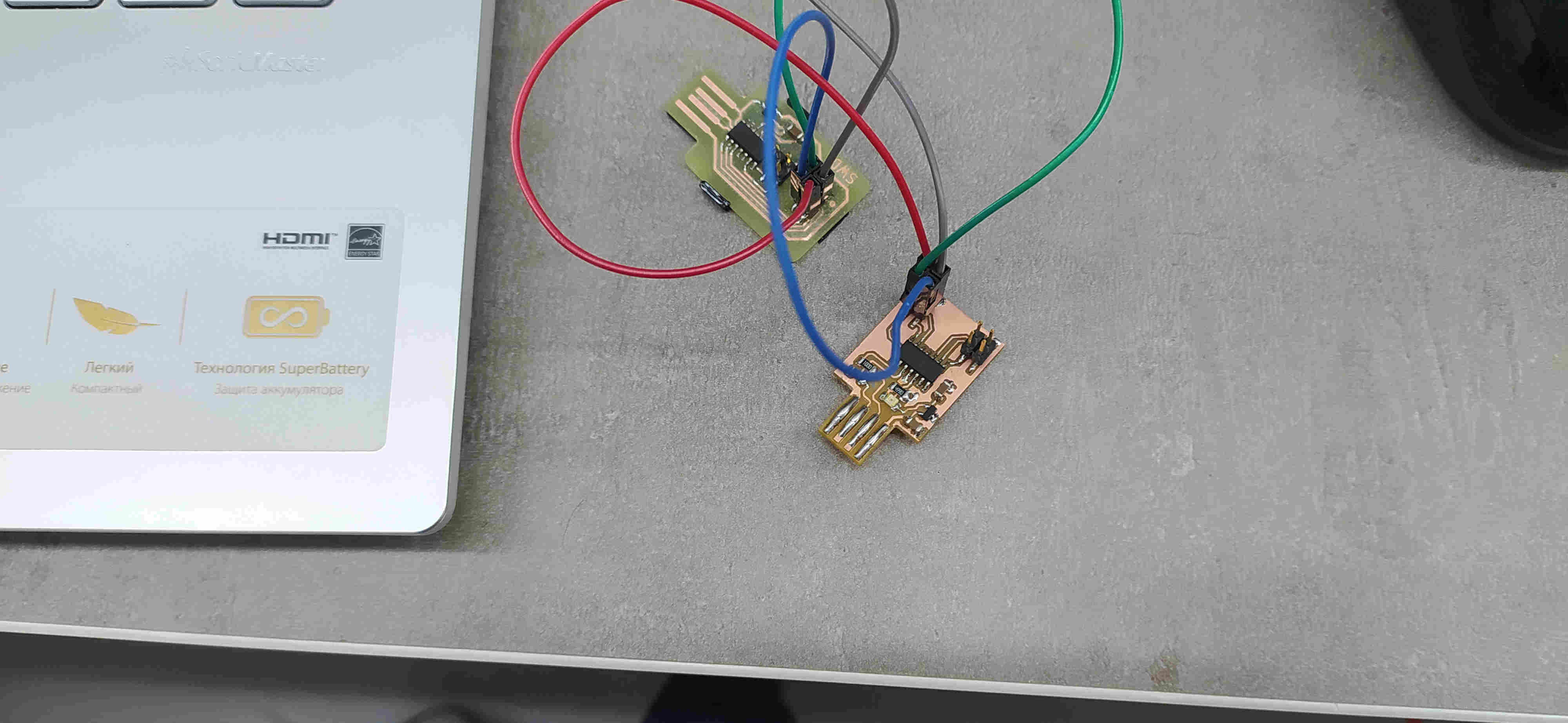
Here is the step-by-step instruction on how to burn the program into my programmer. So, in our Fablab, we had two PCBs that use samd11c one programmer that Babken brought from Finland and one PCB that he designed. I used that programmer from Finland to program my own.
This is programmer from Finland.
First, I need to download the EDBG programmer from here and build it.
Then you need to go to the folder where is the EDBG and run make all commands to build it.
Then on the Fab Academy page (Embedded Programming), we will find the Free Dap bootloader that we will also download. The bootloader has to be inside the EDBG folder.
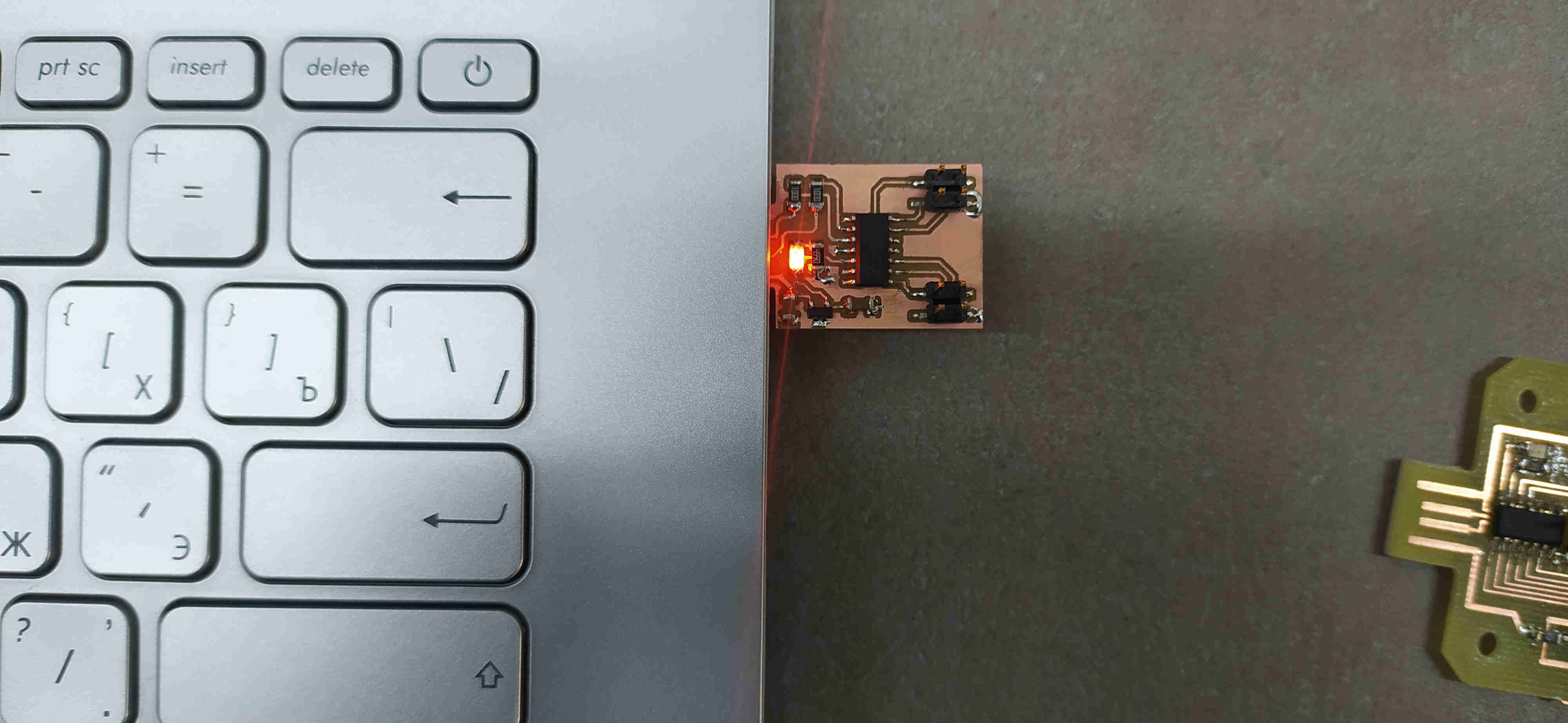
Before programming I need to connect my board and programmer.
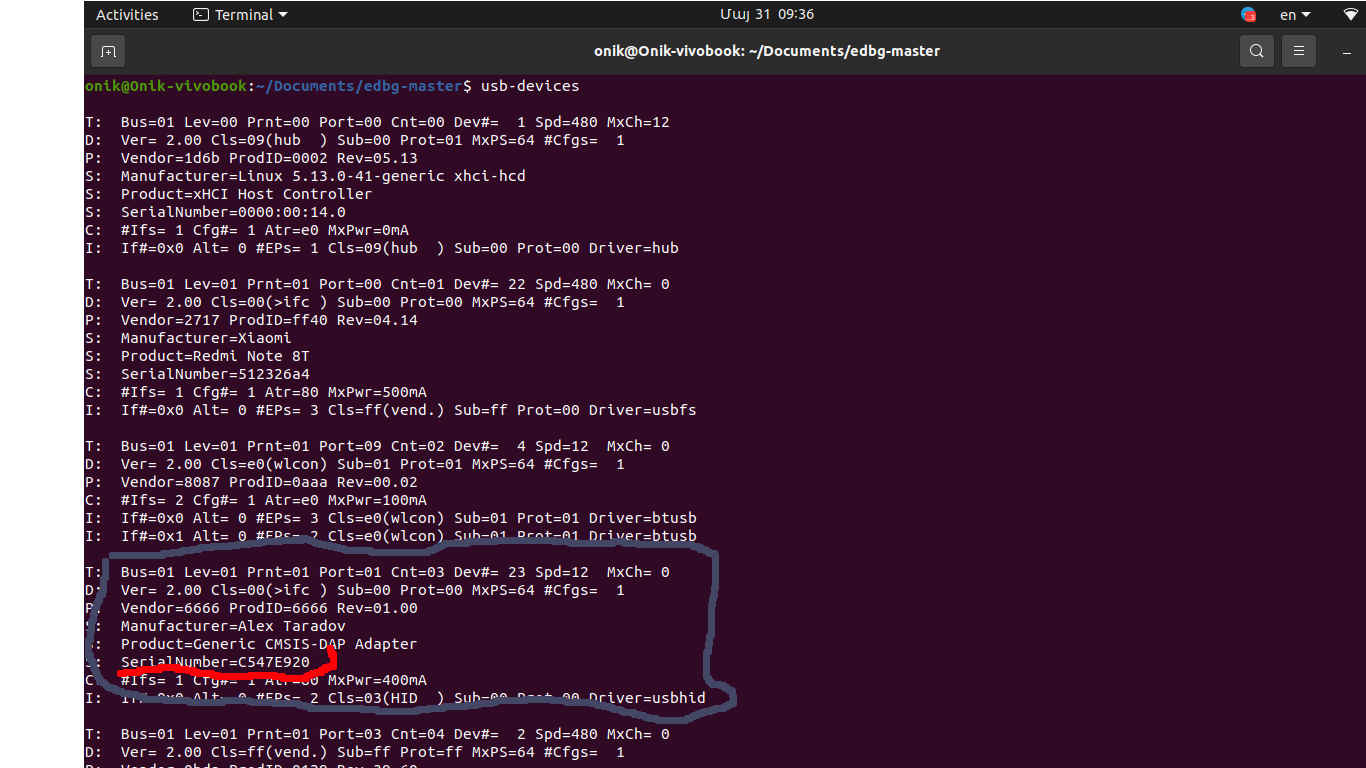
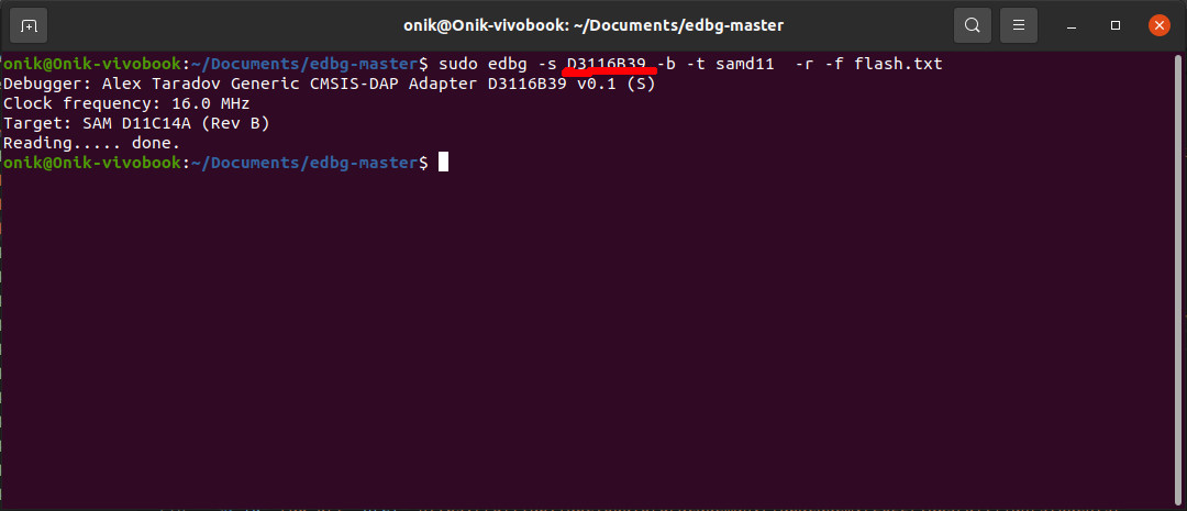
Then in the EDBG folder, I need to place a free dap programmer and before programming, you need to know the serial number of your programmer. So, to know the serial number you should connect it and then type the usb-devices command.
After having all the staff seted we run the programmer.

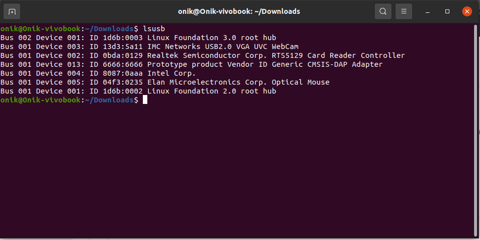
As you can notice I used the serial number of a programmer in the command. So, after programming I need to check is it working. I disconnected the Finland programmer and connected mine and used lsusb to see if it is recognized by the computer.
Then, I used my own programmer to read the flash memory of Babken’s Board. Here you can see my programmer connected to the Babken’s Board.
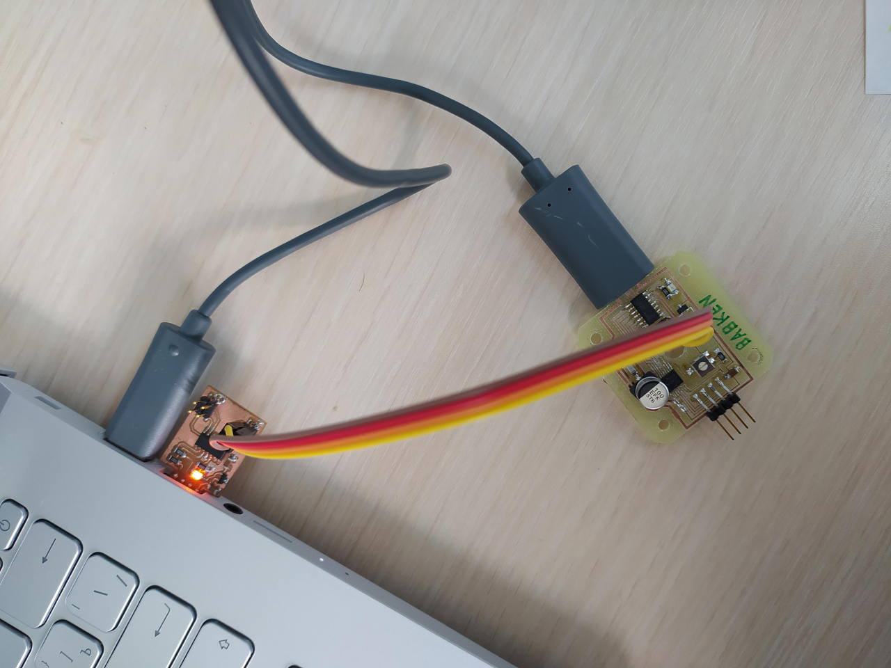
You can notice that I changed the serial number of a programmer. Finally, I have a working programmer that I am going to use in the next weeks.