5. Electronics production
Group assignment: characterize the design rules for your in-house PCB production process extra credit: send a PCB out to a board house
Research
After doing trial soldering, we had some explanation in a group about PCBs, what is that for, components, what do they do, etc.
 To not waste the time and material, we decided to cut both line test and PCB base on the same material. Line test is for testing the machine and finding out the thickness of the lines it can handle, which can’t be cut out, the tool can’t enter and cut there. For that we did the following steps:
1. READ the machine user manual , how it works the safety rules, etc.
2. Using two sided tape, attach the material to the table. For best result use clamps to improve adhesion.
3. Download the .png files in our case linetest.
Traces for linetest
Cutout for linetest
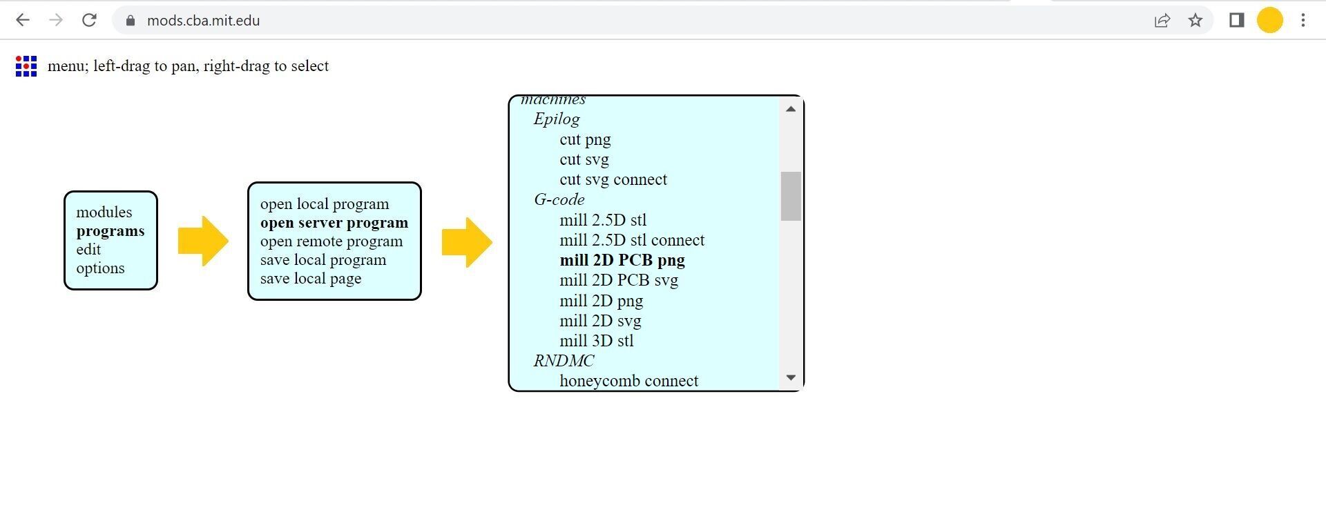
4. Go to mods.cba.mit.edu In the mods page, the png file can be converted to .nc file (numeric control Gcode file) necessary for the CNC machine to execute the milling process.
Here are steps to get to 2D PCB milling for png files.
To not waste the time and material, we decided to cut both line test and PCB base on the same material. Line test is for testing the machine and finding out the thickness of the lines it can handle, which can’t be cut out, the tool can’t enter and cut there. For that we did the following steps:
1. READ the machine user manual , how it works the safety rules, etc.
2. Using two sided tape, attach the material to the table. For best result use clamps to improve adhesion.
3. Download the .png files in our case linetest.
Traces for linetest
Cutout for linetest
4. Go to mods.cba.mit.edu In the mods page, the png file can be converted to .nc file (numeric control Gcode file) necessary for the CNC machine to execute the milling process.
Here are steps to get to 2D PCB milling for png files.
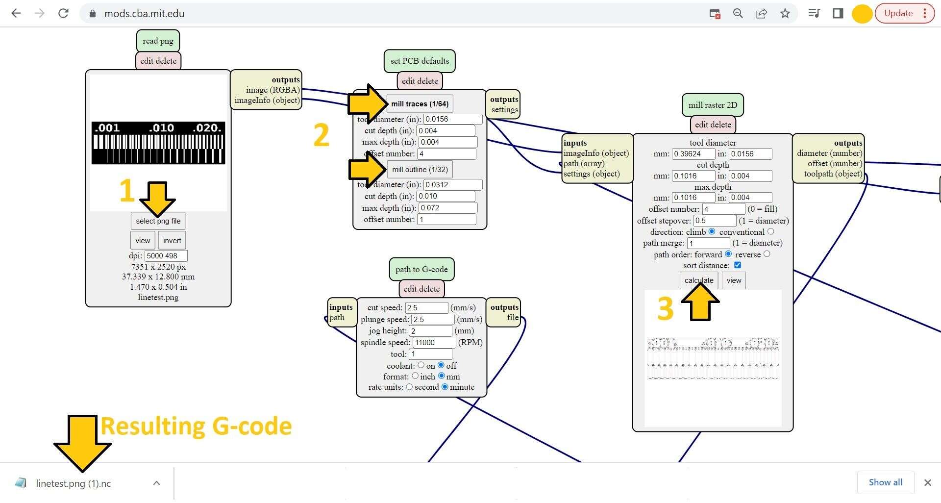
 Select the file then select the process first mill the traces then cutout. We need two separate G-codes for each process and we need to change the tool. 1/64” for traces and 1/32” for cutout.
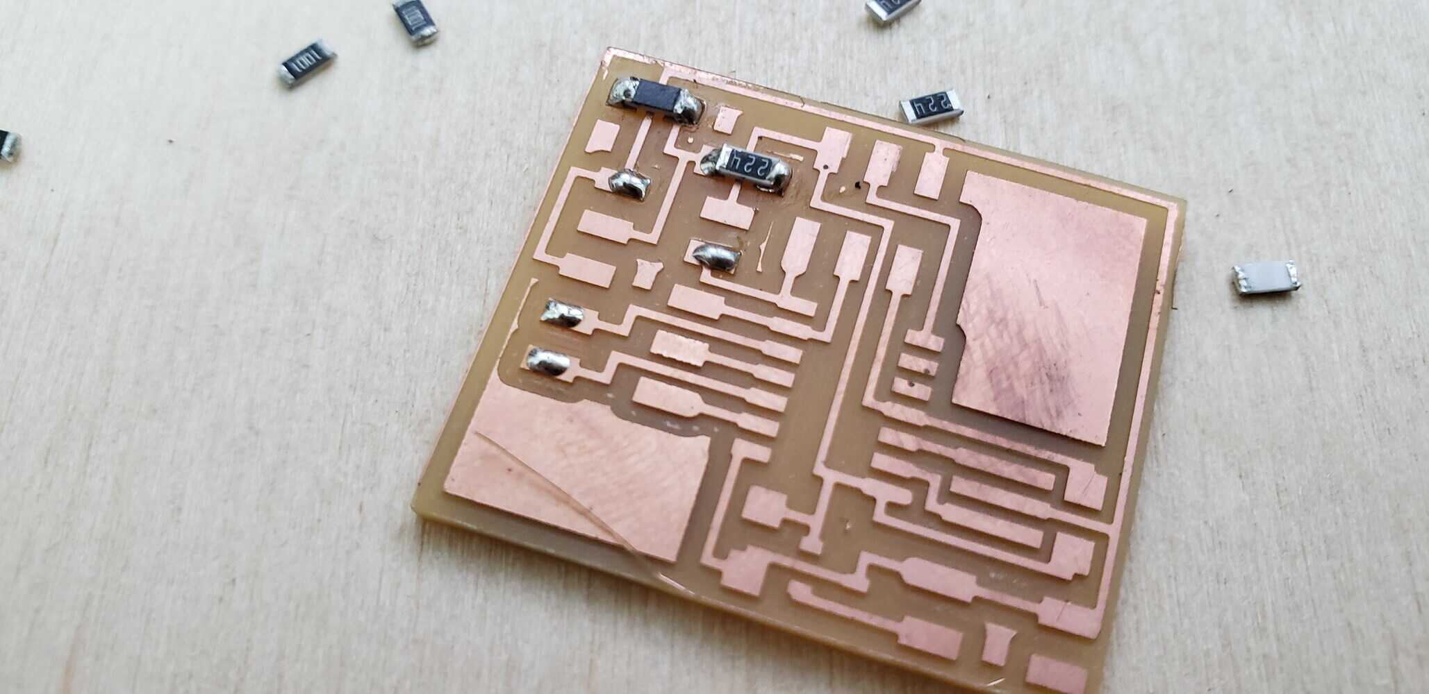
 After cutting the linetest we got this result.
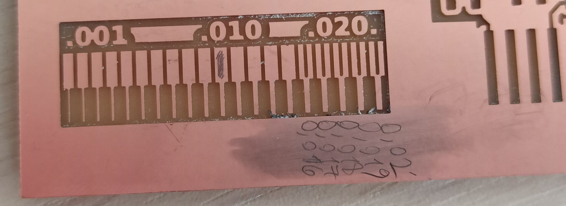 The linetest is using inches.
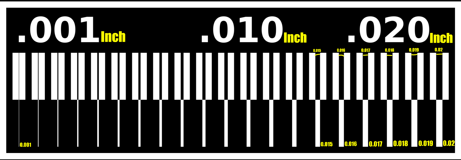 As we can see our 1/64” (0.3969mm) endmill didn’t cut after 0.016inches (0.4064mm).
So while designing a PCB we must take this into account that if traces are closer than 0.4mm our endmill wouldn’t mill those and we’ll endup with fused tracks.
As we can see our 1/64” (0.3969mm) endmill didn’t cut after 0.016inches (0.4064mm).
So while designing a PCB we must take this into account that if traces are closer than 0.4mm our endmill wouldn’t mill those and we’ll endup with fused tracks.